1. A clean single crystal silicon (Si) wafer which is doped n-type (ColumnV elements of the periodic...
22
1. A clean single crystal silicon (Si) wafer which is doped n-type (ColumnV elements of the periodic table). MOS devices are typically fabricated on a <100>, in the X-cut direction to
-
Upload
julian-wilkerson -
Category
Documents
-
view
215 -
download
2
Transcript of 1. A clean single crystal silicon (Si) wafer which is doped n-type (ColumnV elements of the periodic...

1. A clean single crystal silicon (Si) wafer which is doped n-type (ColumnV elements of the periodic table). MOS devices are typically fabricated on a <100>, in the X-cut direction to minimize surface state charges.
2. A 2” diameter clean single crystal silicon (Si) wafer which represents a single molecule having a diamond lattice structure. The wafer-flat is used for alignment.
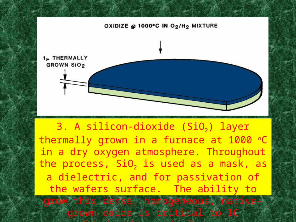
3. A silicon-dioxide (SiO2) layer thermally grown in a furnace at 1000 oC in a dry oxygen atmosphere.
Throughout the process, SiO2 is used as a mask, as a dielectric, and for passivation of the wafers surface. The ability to grow this dense, homogeneous, native-grown
oxide is critical to IC fabrication technology.
4. A thermally grown SiO2 layer on a Si wafer. The SiO2 is transparent; the color comes from light-interference from
reflection at the Si-SiO2 interface and the SiO2-air interface.

5. Photoresist is spun onto the wafer at 3500 rpm for 30 seconds. The wafer is soft-baked at 90 oC for 30 minutes; leaving a thin, photo-sensitive film. The film is sensitive
to ultraviolet (UV) light; this is why fabrication laboratories are often lit by UV-absent, yellow light.
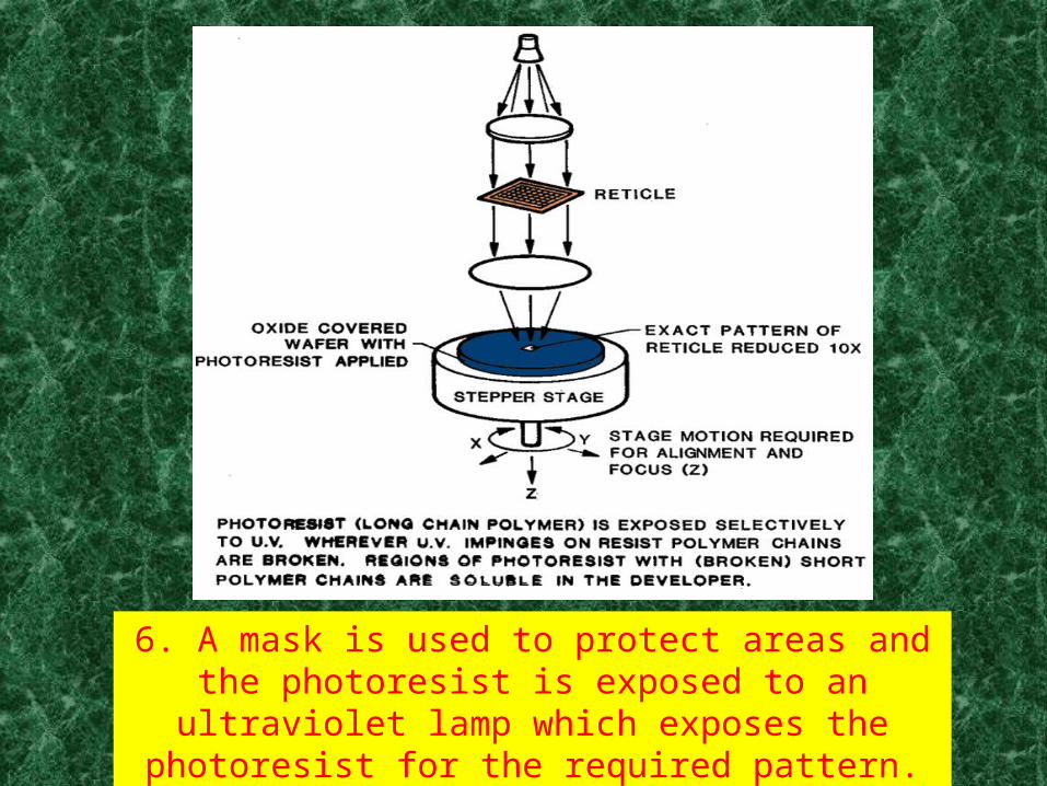
6. A mask is used to protect areas and the photoresist is exposed to an ultraviolet lamp which exposes the
photoresist for the required pattern.
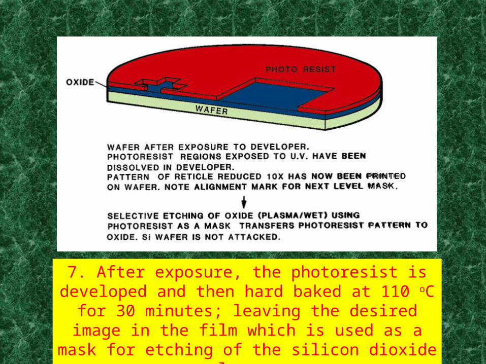
7. After exposure, the photoresist is developed and then hard baked at 110 oC for 30 minutes; leaving the desired image in the film which is used as a mask for etching of
the silicon dioxide layer.
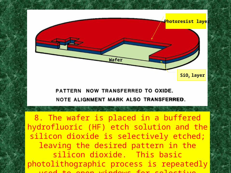
8. The wafer is placed in a buffered hydrofluoric (HF) etch solution and the silicon dioxide is selectively etched;
leaving the desired pattern in the silicon dioxide. This basic photolithographic process is repeatedly used to open
windows for selective processing at the silicon surface.
Photoresist layer
SiO2 layer
Wafer
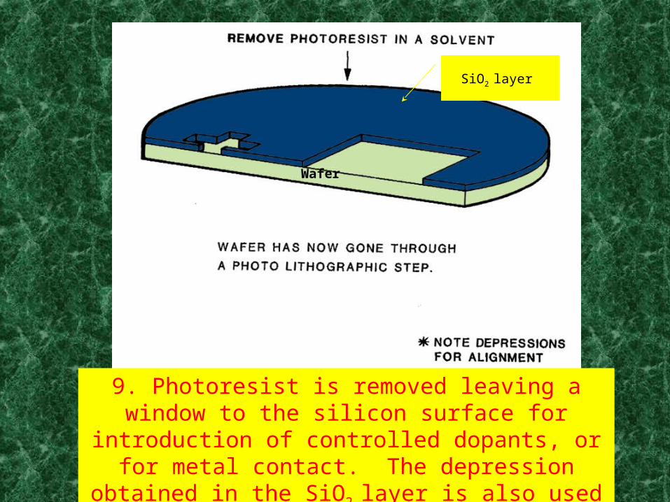
9. Photoresist is removed leaving a window to the silicon surface for introduction of controlled dopants, or for
metal contact. The depression obtained in the SiO2 layer is also used for alignment from level-to-level in the
process.
SiO2 layer
Wafer
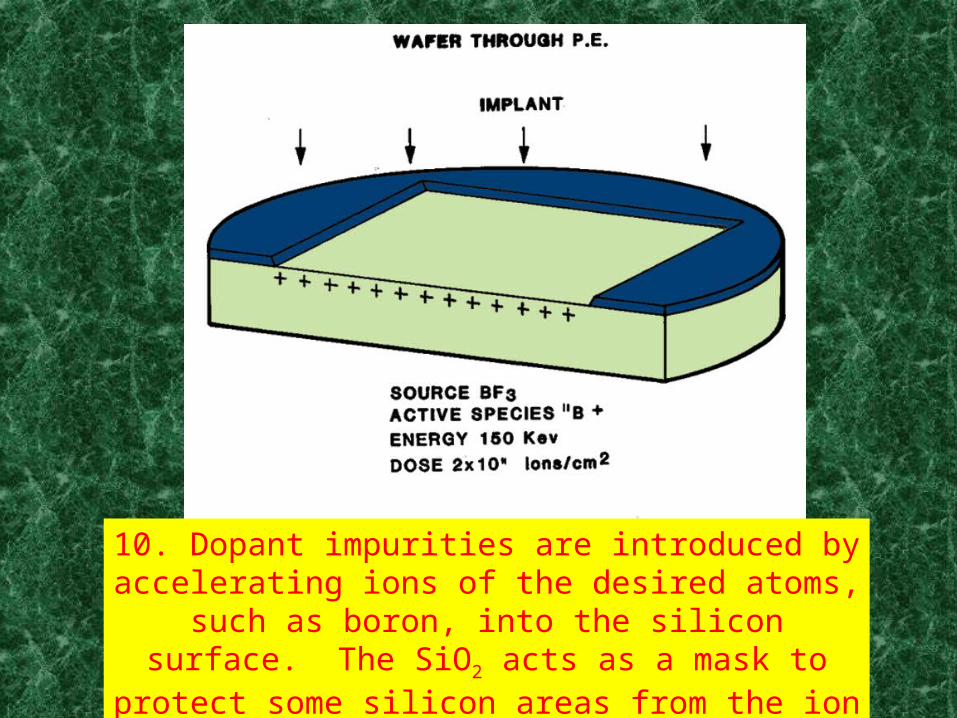
10. Dopant impurities are introduced by accelerating ions of the desired atoms, such as boron, into the silicon
surface. The SiO2 acts as a mask to protect some silicon areas from the ion implantation.
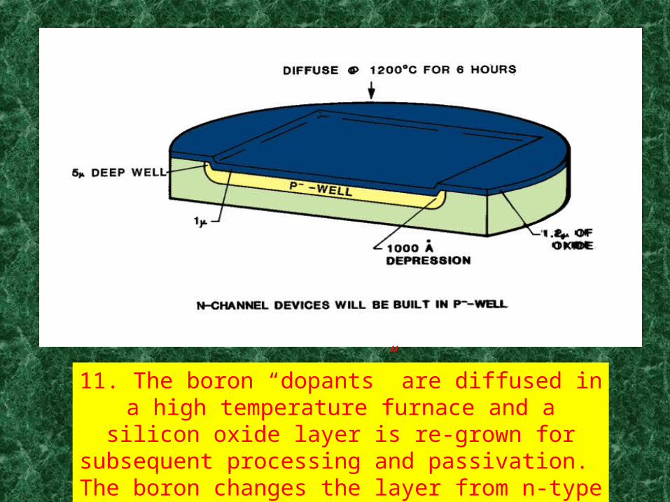
11. The boron “dopants” are diffused in a high temperature furnace and a silicon oxide layer is re-grown
for subsequent processing and passivation. The boron changes the layer from n-type to p-type material.
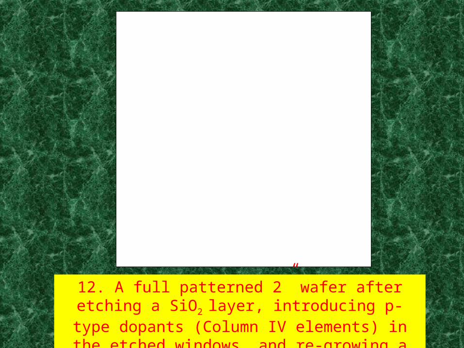
12. A full patterned 2” wafer after etching a SiO2 layer, introducing p-type dopants (Column IV elements) in the
etched windows, and re-growing a second SiO2 layer.
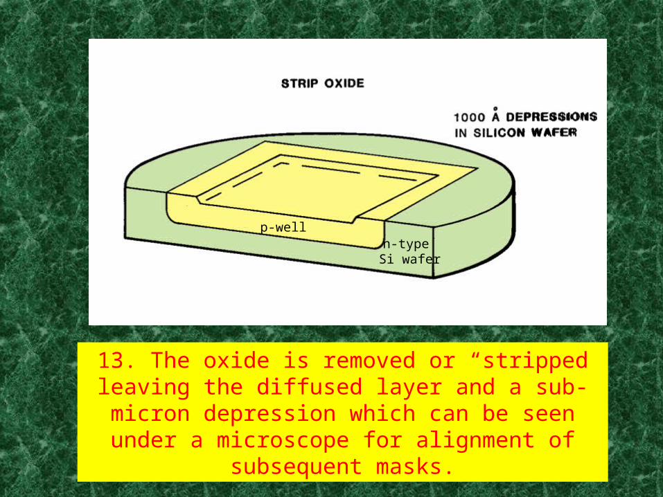
13. The oxide is removed or “stripped leaving the diffused layer and a sub-micron depression which can be
seen under a microscope for alignment of subsequent masks.
p-welln-type
Si wafer
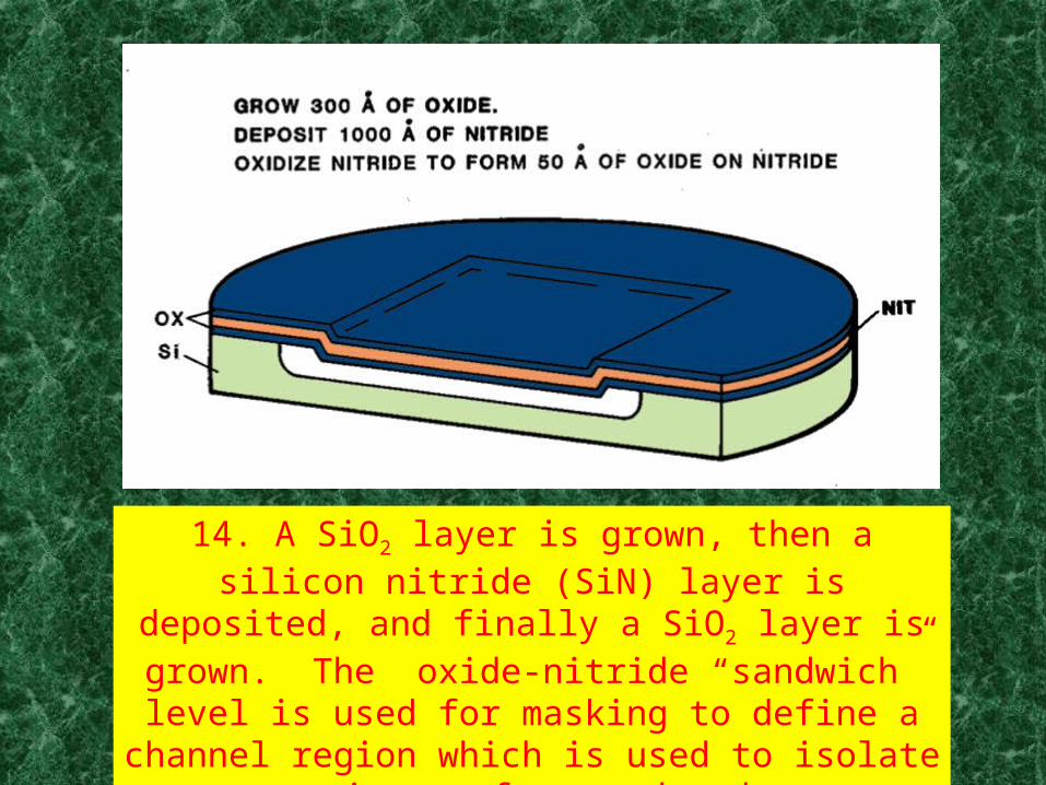
14. A SiO2 layer is grown, then a silicon nitride (SiN) layer is deposited, and finally a SiO2 layer is grown. The
oxide-nitride “sandwich” level is used for masking to define a channel region which is used to isolate transistors
from each other.

15. A buffered HF etch removes the exposed SiO2. The SiN masks and protects the underlying SiO2 and Si
surface. The wafer is then ion implanted with boron atoms to define the channel stop areas.
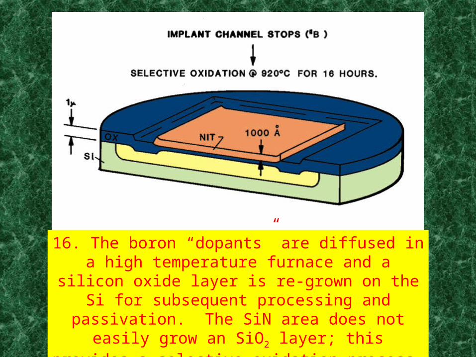
16. The boron “dopants” are diffused in a high temperature furnace and a silicon oxide layer is re-grown on the Si for subsequent processing and passivation. The SiN area does not easily grow an SiO2 layer; this provides
a selective oxidation process.
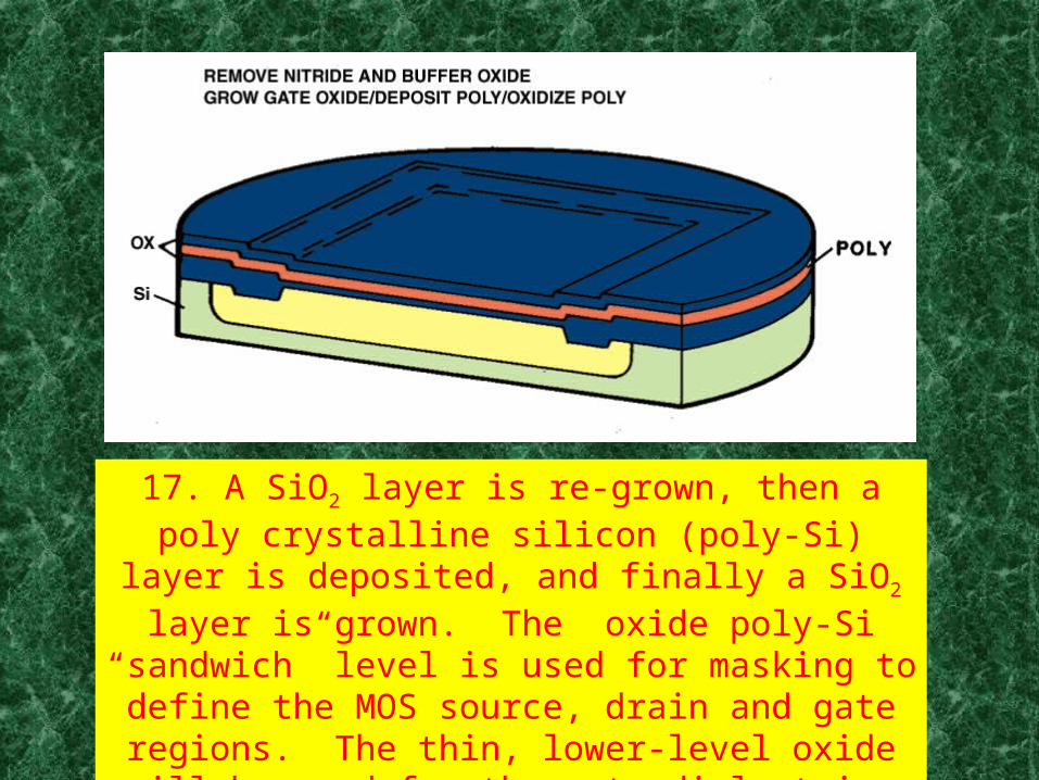
17. A SiO2 layer is re-grown, then a poly crystalline silicon (poly-Si) layer is deposited, and finally a SiO2
layer is grown. The oxide poly-Si “sandwich” level is used for masking to define the MOS source, drain and
gate regions. The thin, lower-level oxide will be used for the gate dielectric.
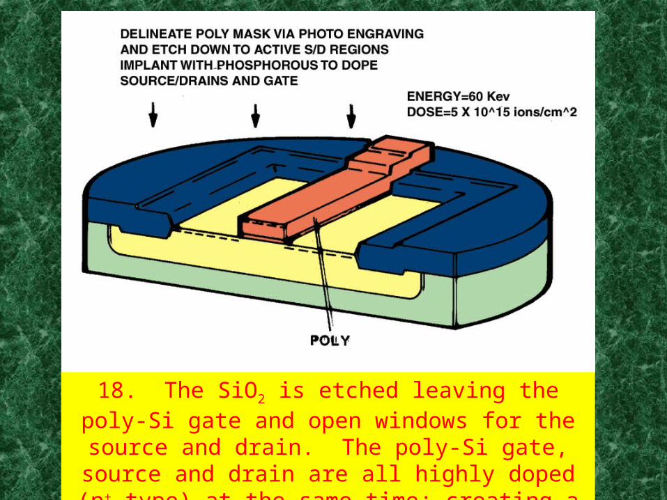
18. The SiO2 is etched leaving the poly-Si gate and open windows for the source and drain. The poly-Si gate, source and drain are all highly doped (n+-type) at the
same time; creating a self-aligned MOS process.
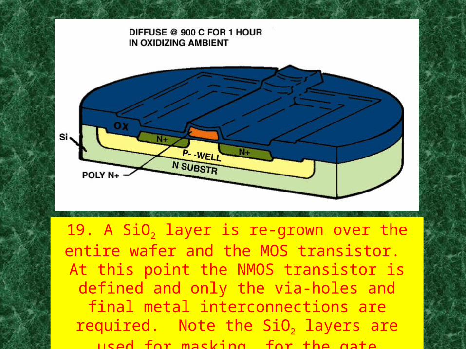
19. A SiO2 layer is re-grown over the entire wafer and the MOS transistor. At this point the NMOS transistor is
defined and only the via-holes and final metal interconnections are required. Note the SiO2 layers are
used for masking, for the gate dielectric and for passivation of the surface.
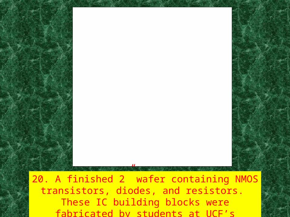
20. A finished 2” wafer containing NMOS transistors, diodes, and resistors. These IC building blocks were
fabricated by students at UCF’s microelectronic facility.
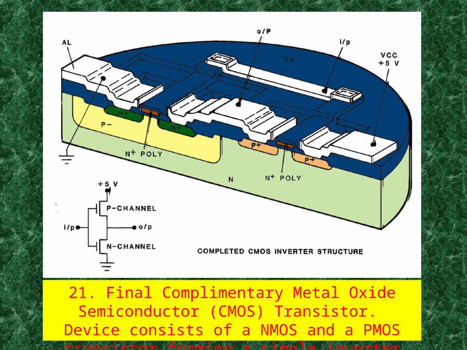
21. Final Complimentary Metal Oxide Semiconductor (CMOS) Transistor. Device consists of a NMOS and a
PMOS transistor forming a simple inverter circuit.
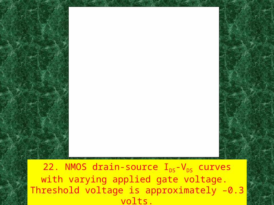
22. NMOS drain-source IDS-VDS curves with varying applied gate voltage. Threshold voltage is approximately
–0.3 volts.
![Unique synthesis of graphene-based materials for clean ... · phene layers from silicon carbide (SiC) or carbon-doped metal substrates [33,34]. SLG or FLG can be fabricated via sublimation](https://static.fdocuments.in/doc/165x107/5e2d4a97a86bdd5aaf6e59a1/unique-synthesis-of-graphene-based-materials-for-clean-phene-layers-from-silicon.jpg)