CMOS Fabrication and Layout - EWU · PDF fileCMOS Fabrication and Layout • Transistors...
39
1 CMOS Fabrication and Layout • Transistors are fabricated on a thin silicon wafer that serve as both a mechanical support and electrical common point called substrate • Fabrication process (a.k.a. Lithography) is similar to printing press – On each step, different materials are deposited or etched • Easiest way to understand physical layout is to look at the wafer from two perspectives: – Top-section – Cross-section
Transcript of CMOS Fabrication and Layout - EWU · PDF fileCMOS Fabrication and Layout • Transistors...

1
CMOS Fabrication and Layout• Transistors are fabricated on a thin silicon wafer that
serve as both a mechanical support and electrical common point called substrate
• Fabrication process (a.k.a. Lithography) is similar to printing press
– On each step, different materials are deposited or etched
• Easiest way to understand physical layout is to look at the wafer from two perspectives:
– Top-section– Cross-section
2
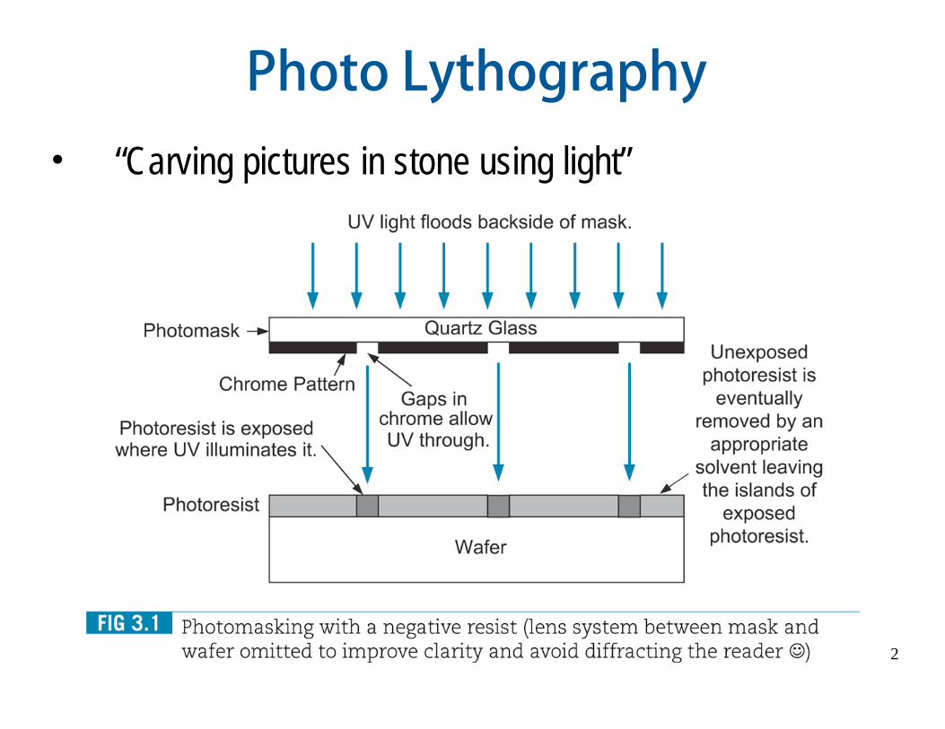
Photo Lythography• “Carving pictures in stone using light”

3
Inverter Cross Section
• Typically use p-type substrate for nMOS transistors
• Requires n-well for body of pMOS transistors
Where is the 4th terminal of each transistor ?

4
Well and Substrate Taps• Substrate must be tied to GND and n-well to VDD
• Metal to lightly-doped semiconductor forms poor connection (parasitic diode)
• Use heavily doped well and substrate contacts

5
Let's add some color ...
n-well
6
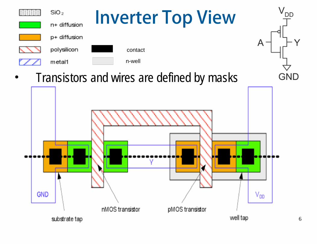
Inverter Top View
• Transistors and wires are defined by masks
contact
n-well

7
Inverter Mask Set
Six masks:
• n-well
• poly silicon
• n+ diffusion
• p+ diffusion
• Contact
• Metal
8
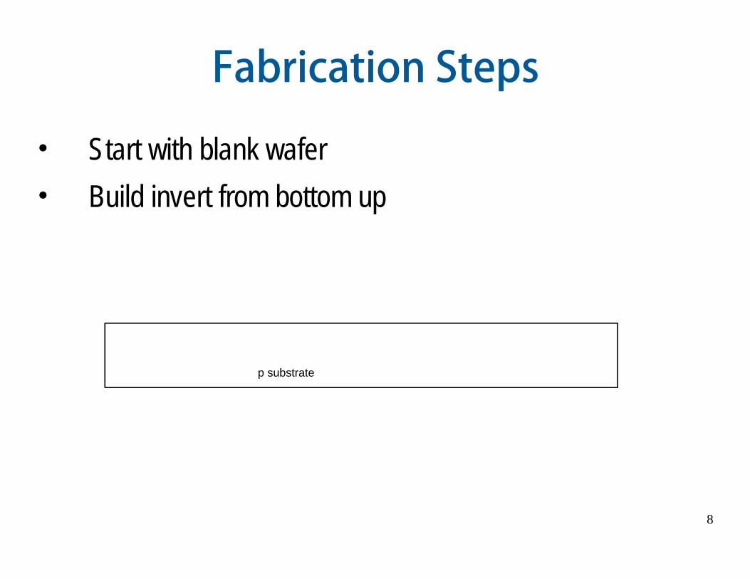
Fabrication Steps
• Start with blank wafer
• Build invert from bottom up
p substrate
9
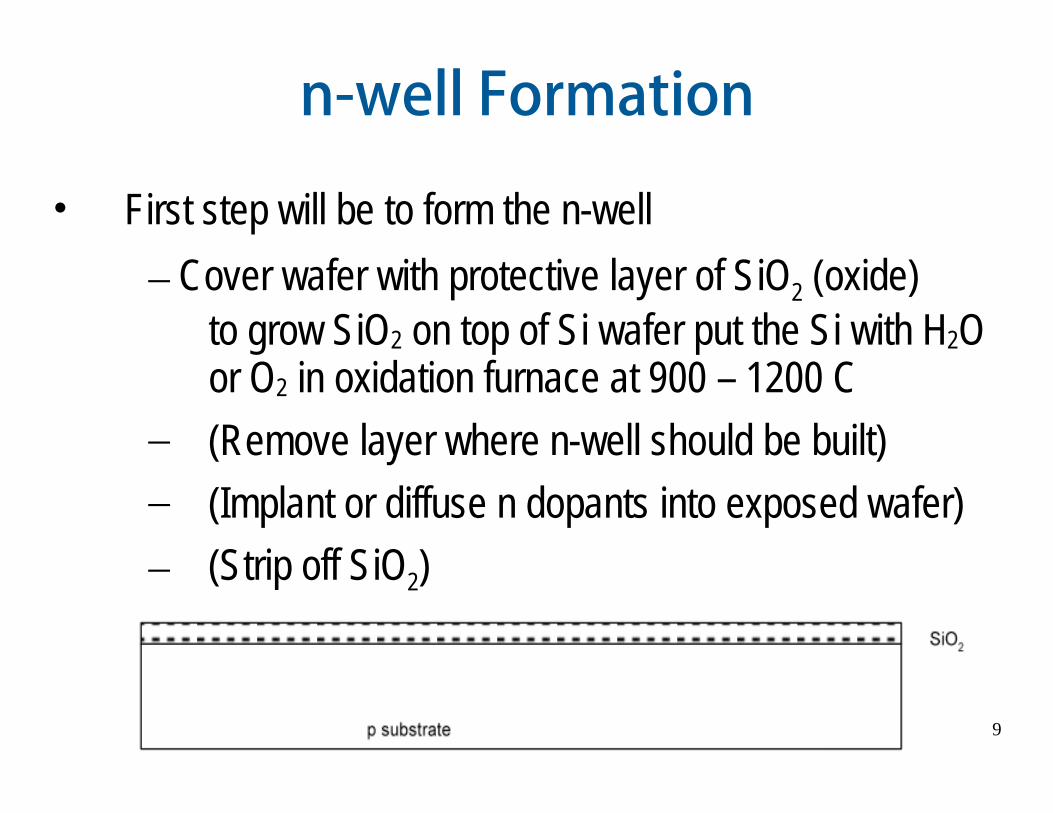
n-well Formation
• First step will be to form the n-well
– Cover wafer with protective layer of SiO2 (oxide)to grow SiO2 on top of Si wafer put the Si with H2O or O2 in oxidation furnace at 900 – 1200 C
– (Remove layer where n-well should be built)– (Implant or diffuse n dopants into exposed wafer)
– (Strip off SiO2)
10
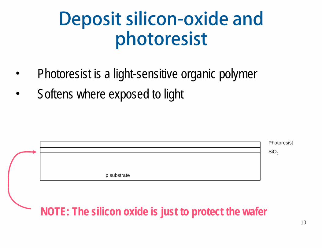
Deposit silicon-oxide and photoresist
• Photoresist is a light-sensitive organic polymer
• Softens where exposed to light
p substrate
SiO2
Photoresist
NOTE: The silicon oxide is just to protect the wafer

11
Photo-Lithography
• Expose photoresist through n-well mask
• Strip off exposed photoresist
p substrate
SiO2
Photoresist

12
Etching
• Etch oxide with hydrofluoric acid (HF)
– Seeps through skin and eats bone: nasty stuff!!!• Only attacks oxide where resist has been exposed
p substrate
SiO2
Photoresist

13
The n-well• n-well is formed with diffusion or ion implantation
• Diffusion
– Place wafer in furnace with arsenic gas– Heat until As atoms diffuse into exposed Si
• Ion Implantation
– Blast wafer with beam of As ions
– Ions blocked by SiO2, only enter exposed Si
n well
SiO2

14
Strip protective oxide
• Strip off the remaining oxide using HF
• Back to bare wafer with n-well
• Subsequent steps involve similar series of steps
p substrate
n well

15
Gate oxide and Polysilicon
• Deposit very thin layer of gate oxide
< 20 Å (6-7 atomic layers)
• Chemical Vapor Deposition (CVD) of silicon layer
– Place wafer in furnace with Silane gas (SiH4)
– Forms many small crystals called polysilicon
– Heavily doped to be good conductor

16
Polysilicon patterning
• Use same lithography process to pattern polysilicon

17
Self-aligned polysilicon gate process
• The polysilicon gate serves as a mask to allow precise alignment of the source and drain with the gate
• Use oxide and masking to expose where n+ dopants should be diffused or implanted
• n-diffusion forms nMOS source, drain, and n-well contact

18
Formation of the n-diffusions
• Pattern oxide and form n+ regions
• Self-aligned process (poysilicon gate) “blocks” diffusion under the gate
• Polysilicon is better than metal for self-aligned gates because it doesn’t melt during later processing

19
The n-diffusions• Historically dopants were diffused
• Usually ion implantation today (but regions are still called diffusion)
• Strip off oxide to complete patterning step
20
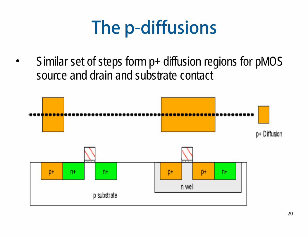
The p-diffusions
• Similar set of steps form p+ diffusion regions for pMOS source and drain and substrate contact

21
Contacts
• Now we need to create the devices' terminals
• Cover chip with thick field oxide (FOX)
• Etch oxide where contact cuts are needed

22
Metallization
• Sputter on aluminum over whole wafer, filling the contacts as well
• Pattern to remove excess metal, leaving wires

23
Fabrication Steps Summary (1/3)

24
Fabrication Steps Summary (2/3)

25
Fabrication Steps Summary (3/3)
FOX

26
Basic Fabrication Steps in a nutshell
• Though a mask transfer an “image” of the design to the wafer
• Do something to imaged parts of the wafer
– Implant – add impurities to change electrical properties
– Deposit – deposit metal, insulator or other layers
– Grow Oxide – place silicon in oxidizing ambient
– Etch – Cut into surface of topmost layer(s)
– Polish – Make surface of wafer flat
• Strip 0ff imaging material (resist) and proceed to next step
27
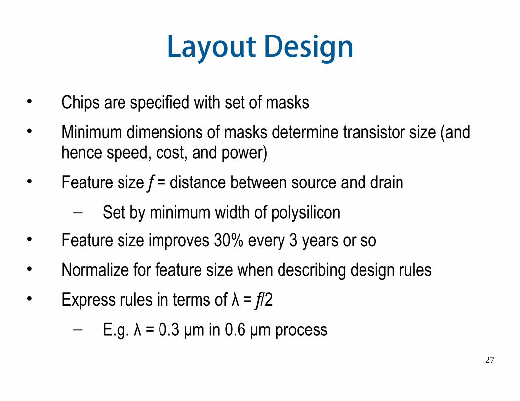
Layout Design
• Chips are specified with set of masks
• Minimum dimensions of masks determine transistor size (and hence speed, cost, and power)
• Feature size f = distance between source and drain
– Set by minimum width of polysilicon
• Feature size improves 30% every 3 years or so
• Normalize for feature size when describing design rules
• Express rules in terms of = f/2
– E.g. = 0.3 μm in 0.6 μm process

28
Layout Design Rules
29
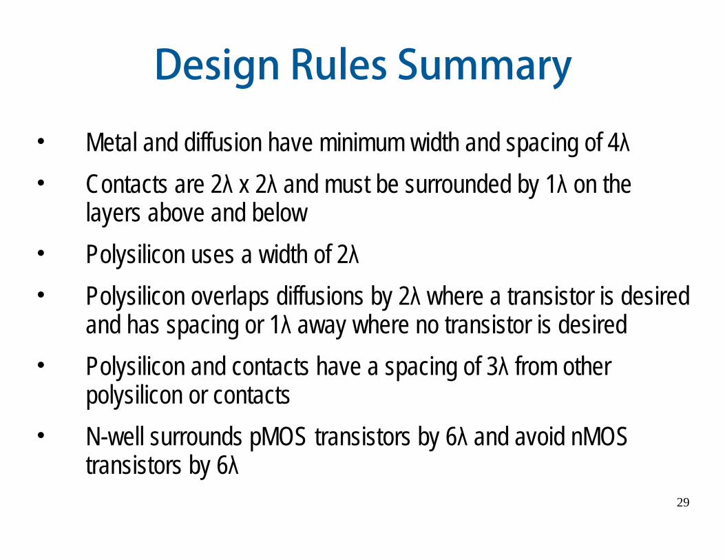
Design Rules Summary
• Metal and diffusion have minimum width and spacing of 4
• Contacts are 2 x 2 and must be surrounded by 1 on the layers above and below
• Polysilicon uses a width of 2
• Polysilicon overlaps diffusions by 2 where a transistor is desired and has spacing or 1 away where no transistor is desired
• Polysilicon and contacts have a spacing of 3 from other polysilicon or contacts
• N-well surrounds pMOS transistors by 6 and avoid nMOS transistors by 6

30
Logic Gates layout
• Layout can be very time consuming
• Design gates to fit together nicely
• Build a library of standard cells
• Standard cell design methodology
– VDD and GND should abut (standard height)
– Adjacent gates should satisfy design rules
– nMOS at bottom and pMOS at top
– All gates include well and substrate contacts
31
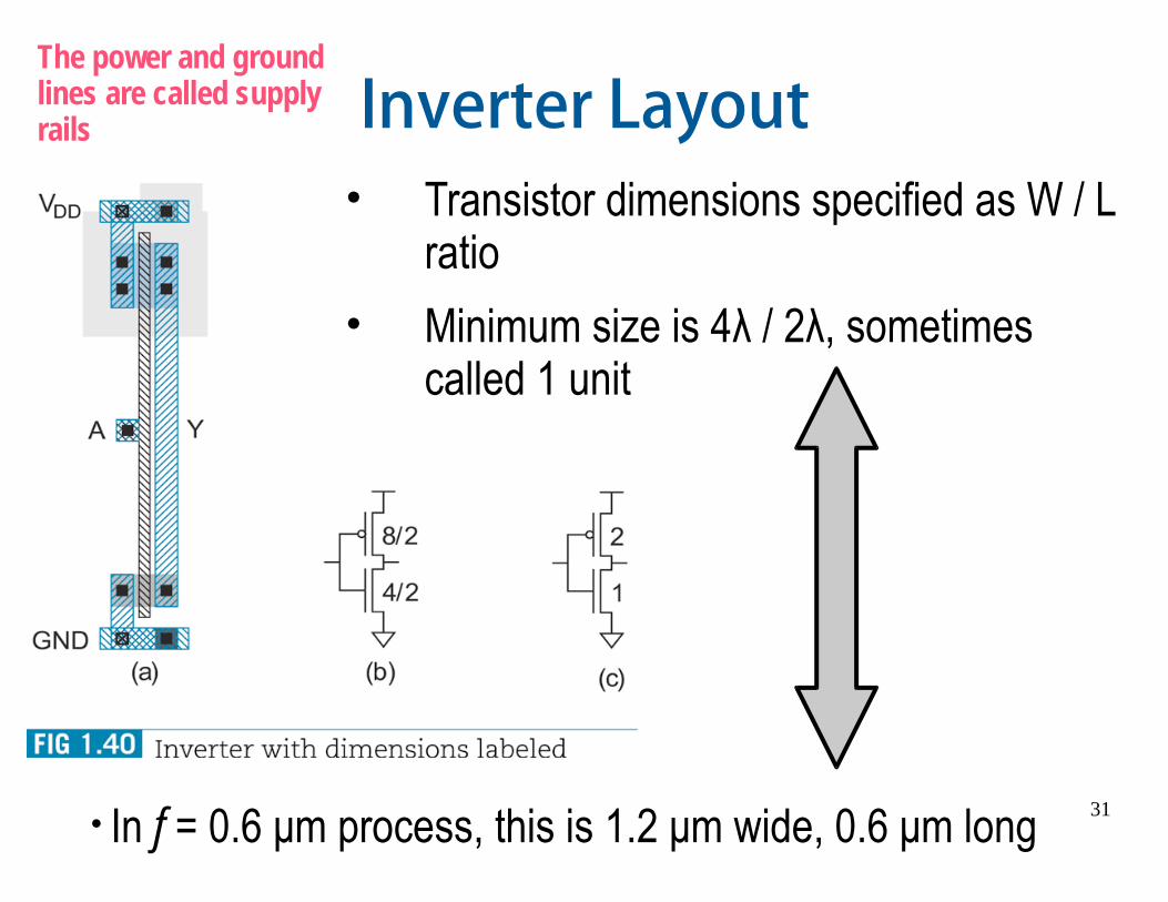
Inverter Layout• Transistor dimensions specified as W / L
ratio
• Minimum size is 4 / 2 , sometimes called 1 unit
• In f = 0.6 μm process, this is 1.2 μm wide, 0.6 μm long
The power and ground lines are called supply rails

32
Inverter Standard Cell Layout
Usually the pMOS haswidth 2 or 3 times the width of the nMOS

33
Inverter Standard Cell Area (1/2)

34
Inverter Standard Cell Area (2)
Three abutted standard cell inverters
35
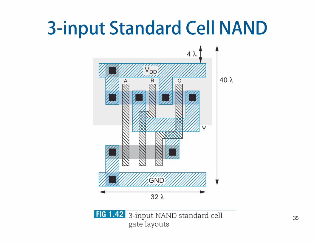
3-input Standard Cell NAND
36
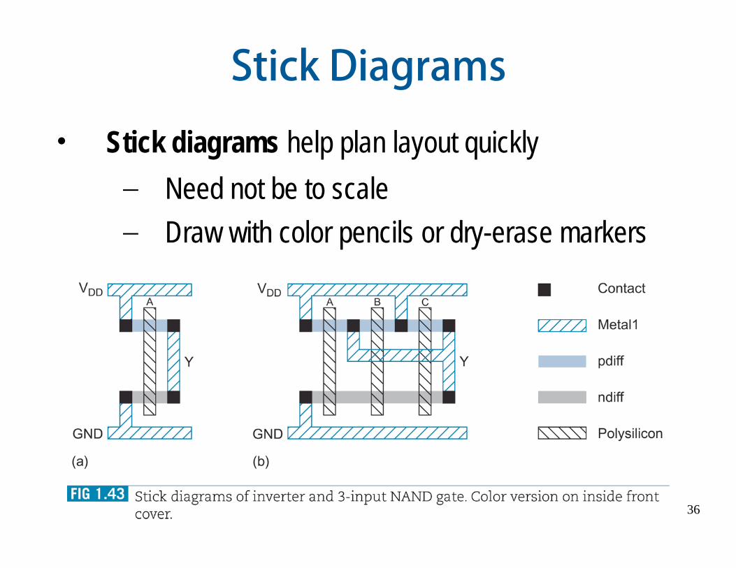
Stick Diagrams
• Stick diagrams help plan layout quickly
– Need not be to scale– Draw with color pencils or dry-erase markers

37
Wiring Tracks
• A wiring track is the space required for a wire
– 4 width, 4 spacing from neighbor = 8 pitch– Transistors also consume one wiring track

38
Well Spacing• Wells must surround transistors by 6
– Implies 12 between opposite transistor flavors– Leaves room for one wire track

39
Area Estimation• Estimate area by counting wiring tracks
– Multiply by 8 to express in