


Languages
Pages
Legal

Chapter 18 - 1
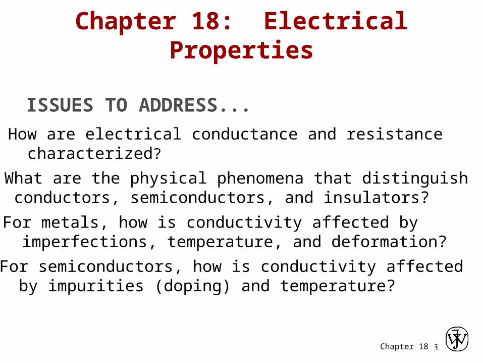
ISSUES TO ADDRESS...
• How are electrical conductance and resistance characterized?
• What are the physical phenomena that distinguish conductors, semiconductors, and insulators?
• For metals, how is conductivity affected by imperfections, temperature, and deformation?
• For semiconductors, how is conductivity affected by impurities (doping) and temperature?
Chapter 18: Electrical Properties

Chapter 18 - 2
• Scanning electron micrographs of an IC:
Fig. (d) from Fig. 12.27(a), Callister & Rethwisch 3e. (Fig. 12.27 is courtesy Nick Gonzales, National Semiconductor Corp., West Jordan, UT.)
• A dot map showing location of Si (a semiconductor): -- Si shows up as light regions.
(b)
View of an Integrated Circuit
0.5 mm
(a)(d)
45 mm
Al
Si (doped)
(d)
• A dot map showing location of Al (a conductor): -- Al shows up as light regions. (c)
Figs. (a), (b), (c) from Fig. 18.27, Callister & Rethwisch 8e.
Chapter 18 - 3
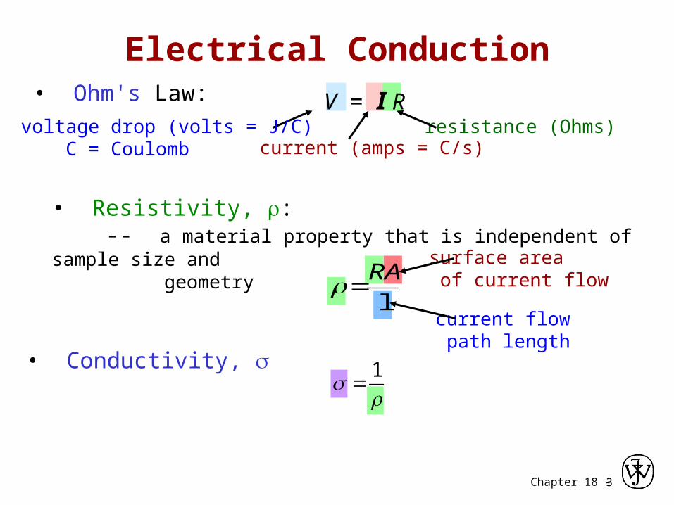
Electrical Conduction• Ohm's Law: V = I R
voltage drop (volts = J/C) C = Coulomb
resistance (Ohms)current (amps = C/s)
1
• Conductivity, s
• Resistivity, r: -- a material property that is independent of sample size and geometry
RA
l
surface area of current flow
current flow path length
Chapter 18 - 4
Electrical Properties
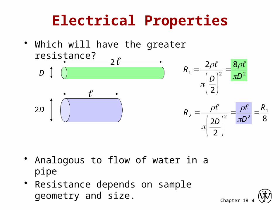
• Which will have the greater resistance?
• Analogous to flow of water in a pipe• Resistance depends on sample geometry and
size.
D
2D
R1 2
D2
2
8D2
2
R2
2D
2
2
D2
R1
8
Chapter 18 - 5
Definitions
Further definitions
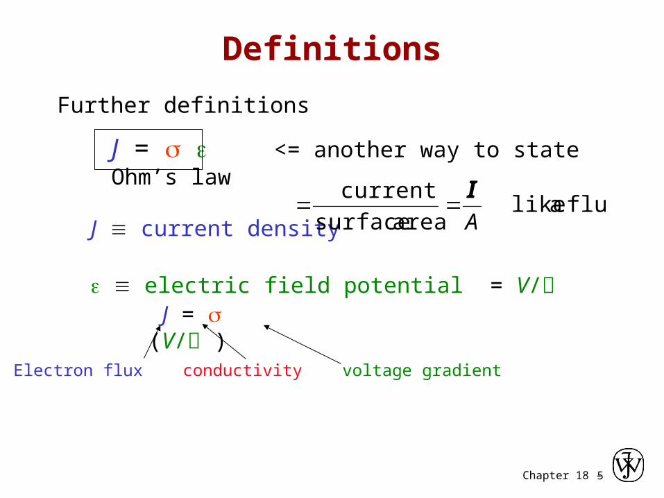
J = <= another way to state Ohm’s law
J current density
electric field potential = V/
flux a like area surface
current
A
I
Electron flux conductivity voltage gradient
J = (V/ )

Chapter 18 - 6
• Room temperature values (Ohm-m)-1 = ( - m)-1
Selected values from Tables 18.1, 18.3, and 18.4, Callister & Rethwisch 8e.
Conductivity: Comparison
Silver 6.8 x 10 7
Copper 6.0 x 10 7
Iron 1.0 x 10 7
METALS conductors
Silicon 4 x 10⁻⁴
Germanium 2 x 10 0
GaAs 10 -6
SEMICONDUCTORS
semiconductors
Polystyrene <10-14
Polyethylene 10-15-10-17
Soda-lime glass 10
Concrete 10-9
Aluminum oxide <10-13
CERAMICS
POLYMERS
insulators
-10-10-11
Chapter 18 - 7
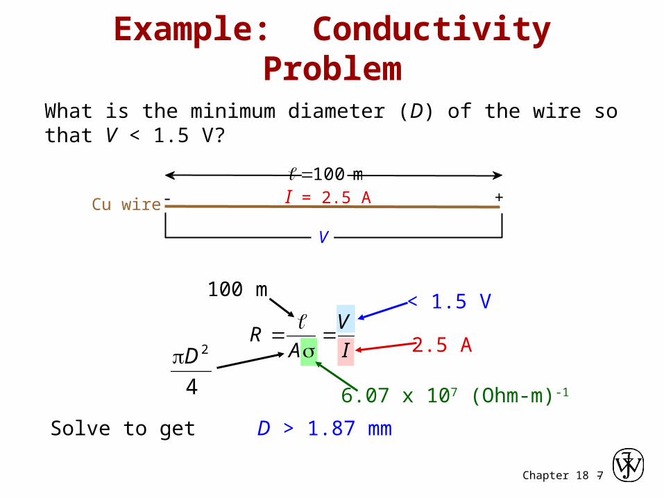
What is the minimum diameter (D) of the wire so that V < 1.5 V?
Example: Conductivity Problem
Cu wire I = 2.5 A- +
V
Solve to get D > 1.87 mm
< 1.5 V
2.5 A
6.07 x 10⁷ (Ohm-m)-1
100 m
I
V
AR
4
2D
100 m

Chapter 18 - 8
Electron Energy Band Structures
Adapted from Fig. 18.2, Callister & Rethwisch 8e.
Chapter 18 - 9
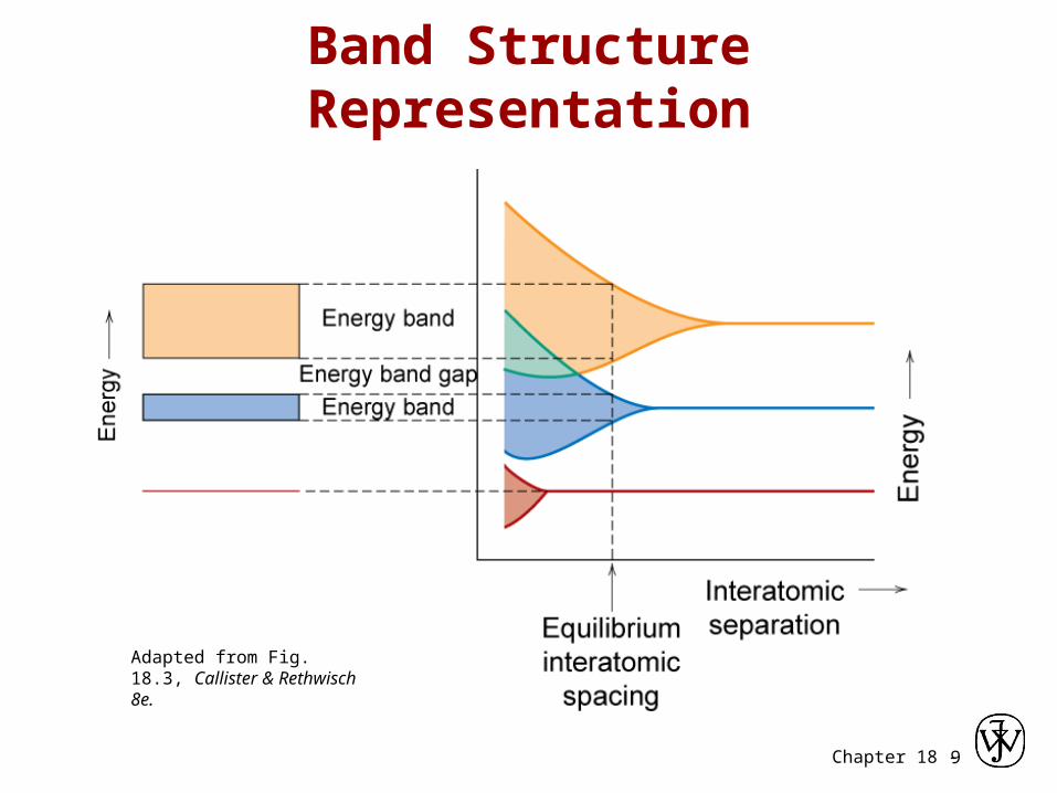
Band Structure Representation
Adapted from Fig. 18.3, Callister & Rethwisch 8e.

Chapter 18 -10
Conduction & Electron Transport• Metals (Conductors):-- for metals empty energy states are adjacent to filled states.
-- two types of band structures for metals
-- thermal energy excites electrons into empty higher energy states.
- partially filled band - empty band that overlaps filled band
filled band
Energy
partly filled band
empty band
GAP
fille
d st
ates
Partially filled band
Energy
filled band
filled band
empty band
fille
d st
ates
Overlapping bands
Chapter 18 -11
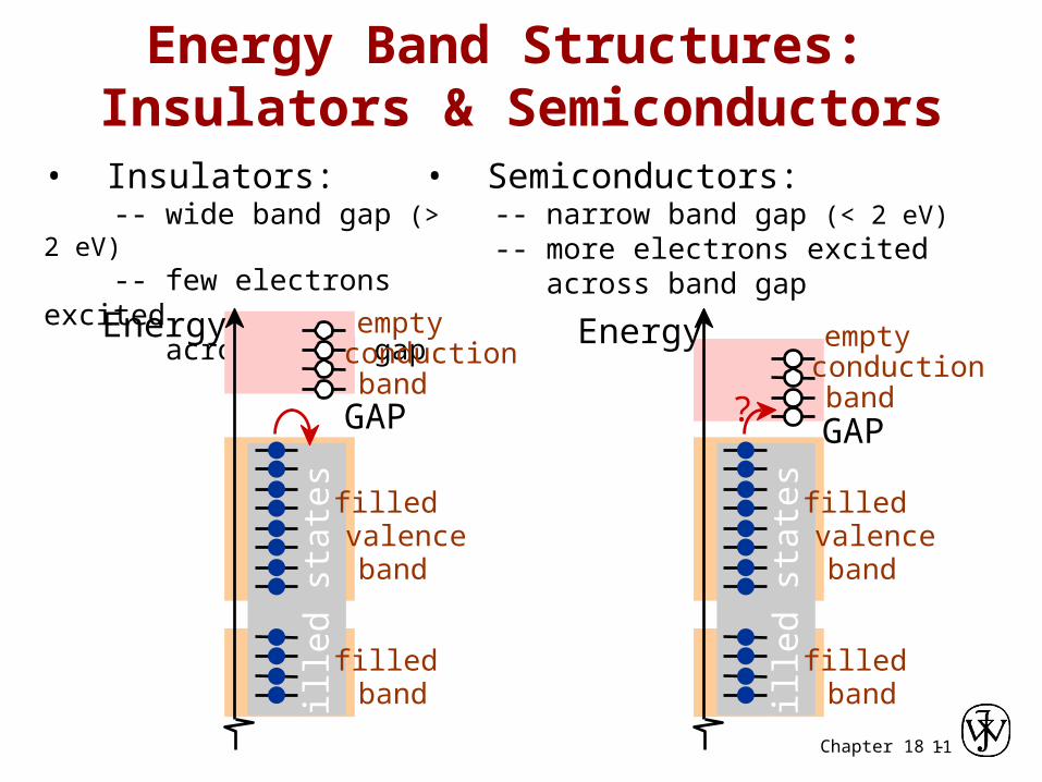
Energy Band Structures: Insulators & Semiconductors
• Insulators: -- wide band gap (> 2 eV) -- few electrons excited across band gap
Energy
filled band
filled valence band
fille
d st
ates
GAP
empty
bandconduction
• Semiconductors: -- narrow band gap (< 2 eV) -- more electrons excited across band gap
Energy
filled band
filled valence band
fille
d st
ates
GAP?
empty
bandconduction
Chapter 18 -12
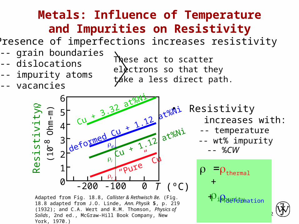
Metals: Influence of Temperature and Impurities on Resistivity
• Presence of imperfections increases resistivity -- grain boundaries -- dislocations -- impurity atoms -- vacancies
These act to scatterelectrons so that theytake a less direct path.
• Resistivity increases with:
=
deformed Cu + 1.12 at%Ni
Adapted from Fig. 18.8, Callister & Rethwisch 8e. (Fig. 18.8 adapted from J.O. Linde, Ann. Physik 5, p. 219 (1932); and C.A. Wert and R.M. Thomson, Physics of Solids, 2nd ed., McGraw-Hill Book Company, New York, 1970.)
T (ºC)-200 -100 0
1
2
3
4
5
6
Res
istiv
ity,
r
(10
-8 O
hm
-m)
0
Cu + 1.12 at%Ni
“Pure” Cu
d -- %CW
+ deformation
i
-- wt% impurity
+ impurity
t
-- temperature
thermal
Cu + 3.32 at%Ni
Chapter 18 -13
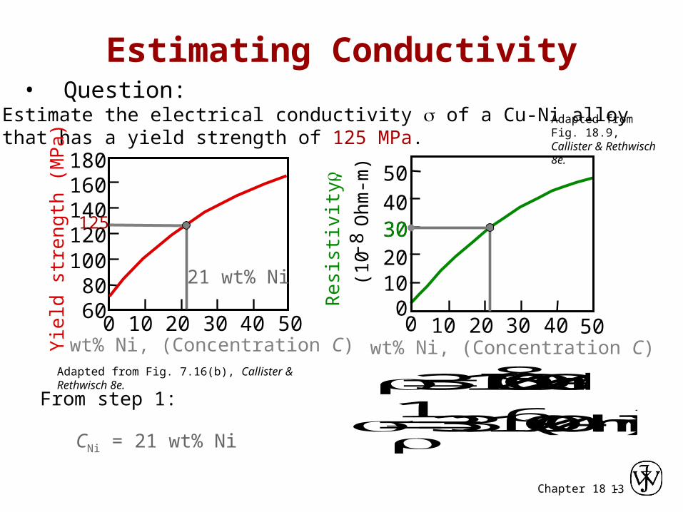
Estimating Conductivity
Adapted from Fig. 7.16(b), Callister & Rethwisch 8e.
• Question:-- Estimate the electrical conductivity of a Cu-Ni alloy that has a yield strength of 125 MPa.
mOhm10 x 30 8
16 )mOhm(10 x 3.31
Yie
ld s
tre
ngt
h (
MP
a)
wt% Ni, (Concentration C)0 10 20 30 40 50
6080
100120140160180
21 wt% Ni
Adapted from Fig. 18.9, Callister & Rethwisch 8e.
wt% Ni, (Concentration C)R
esi
stiv
ity,
r
(10
-8 O
hm
-m)
10 20 30 40 500
10203040
50
0
125
CNi = 21 wt% Ni
From step 1:
30
Chapter 18 -14
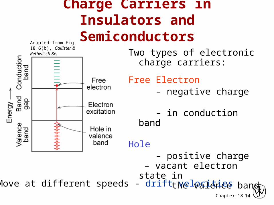
Charge Carriers in Insulators and Semiconductors
Two types of electronic charge carriers:
Free Electron – negative charge – in conduction band
Hole – positive charge
– vacant electron state in the valence band
Adapted from Fig. 18.6(b), Callister & Rethwisch 8e.
Move at different speeds - drift velocities
Chapter 18 -15
Intrinsic Semiconductors
• Pure material semiconductors: e.g., silicon & germanium– Group IVA materials
• Compound semiconductors – III-V compounds
• Ex: GaAs & InSb
– II-VI compounds• Ex: CdS & ZnTe
– The wider the electronegativity difference between the elements the wider the energy gap.
Chapter 18 -16
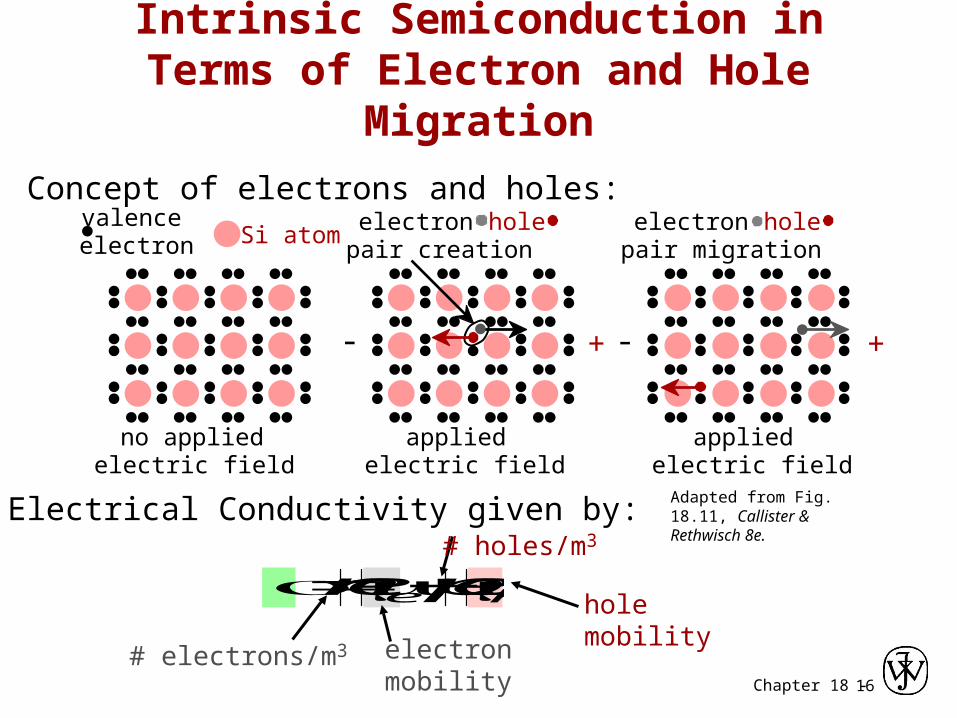
Intrinsic Semiconduction in Terms of Electron and Hole Migration
Adapted from Fig. 18.11, Callister & Rethwisch 8e.
electric field electric field electric field
• Electrical Conductivity given by:
# electrons/m3 electron mobility
# holes/m3
hole mobilityhe epen
• Concept of electrons and holes:
+-
electron hole pair creation
+-
no applied applied
valence electron Si atom
applied
electron hole pair migration
Chapter 18 -17
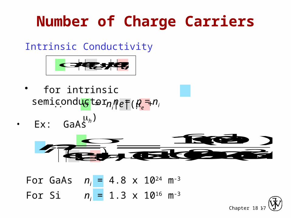
Number of Charge Carriers
Intrinsic Conductivity
)s/Vm 45.085.0)(C10x6.1(
m)(10219
16
hei e
n
For GaAs ni = 4.8 x 1024 m-3
For Si ni = 1.3 x 10¹⁶ m-3
• Ex: GaAs
he epen
• for intrinsic semiconductor n = p = ni = ni|e|(e + h)
Chapter 18 -18
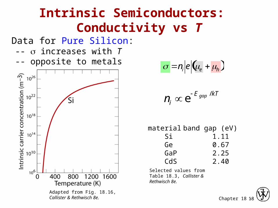
Intrinsic Semiconductors: Conductivity vs T
• Data for Pure Silicon: -- s increases with T -- opposite to metals
Adapted from Fig. 18.16, Callister & Rethwisch 8e.
material Si Ge GaP CdS
band gap (eV) 1.11 0.67 2.25 2.40
Selected values from Table 18.3, Callister & Rethwisch 8e.
ni e Egap / kT
ni e e h
Chapter 18 -19
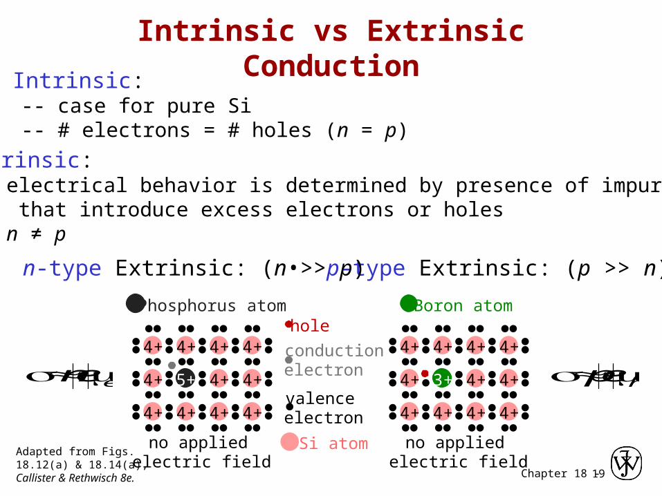
• Intrinsic: -- case for pure Si -- # electrons = # holes (n = p)
• Extrinsic: -- electrical behavior is determined by presence of impurities that introduce excess electrons or holes -- n ≠ p
Intrinsic vs Extrinsic Conduction
3+
• p-type Extrinsic: (p >> n)
no applied electric field
Boron atom
4+ 4+ 4+ 4+
4+
4+4+4+4+
4+ 4+ hep
hole
• n-type Extrinsic: (n >> p)
no applied electric field
5+
4+ 4+ 4+ 4+
4+
4+4+4+4+
4+ 4+
Phosphorus atom
valence electron
Si atom
conductionelectron
een
Adapted from Figs. 18.12(a) & 18.14(a), Callister & Rethwisch 8e.
Chapter 18 -20
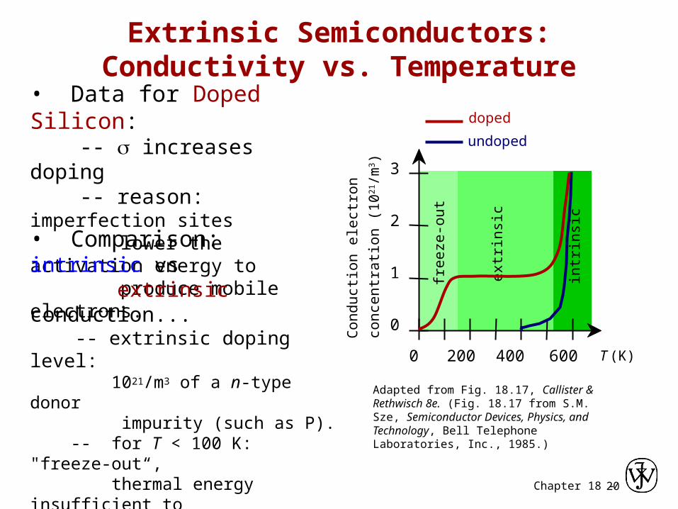
Extrinsic Semiconductors: Conductivity vs. Temperature
• Data for Doped Silicon: -- s increases doping -- reason: imperfection sites lower the activation energy to produce mobile electrons.
• Comparison: intrinsic vs extrinsic conduction... -- extrinsic doping level: 1021/m3 of a n-type donor impurity (such as P). -- for T < 100 K: "freeze-out“, thermal energy insufficient to excite electrons. -- for 150 K < T < 450 K: "extrinsic" -- for T >> 450 K: "intrinsic"
Adapted from Fig. 18.17, Callister & Rethwisch 8e. (Fig. 18.17 from S.M. Sze, Semiconductor Devices, Physics, and Technology, Bell Telephone Laboratories, Inc., 1985.)
Co
nd
uct
ion
ele
ctro
n
con
cen
tra
tion
(1
021/m
3 )T (K)6004002000
0
1
2
3
fre
eze
-ou
t
ext
rin
sic
intr
insi
c
doped
undoped
Chapter 18 -21
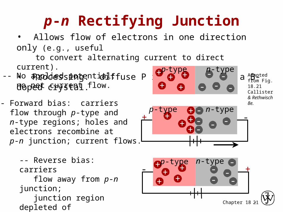
• Allows flow of electrons in one direction only (e.g., useful to convert alternating current to direct current).• Processing: diffuse P into one side of a B-doped crystal.
-- No applied potential: no net current flow.
-- Forward bias: carriers flow through p-type and n-type regions; holes and electrons recombine at p-n junction; current flows.
-- Reverse bias: carriers flow away from p-n junction; junction region depleted of carriers; little current flow.
p-n Rectifying Junction
++
++
+- ---
-p-type n-type
+ -
++ +
++
--
--
-
p-type n-typeAdapted from Fig. 18.21 Callister & Rethwisch 8e.
+++
+
+
---
--
p-type n-type- +
Chapter 18 -22
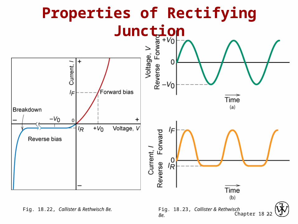
Properties of Rectifying Junction
Fig. 18.22, Callister & Rethwisch 8e. Fig. 18.23, Callister & Rethwisch 8e.

Chapter 18 -23
Junction Transistor
Fig. 18.24, Callister & Rethwisch 8e.
Chapter 18 -24
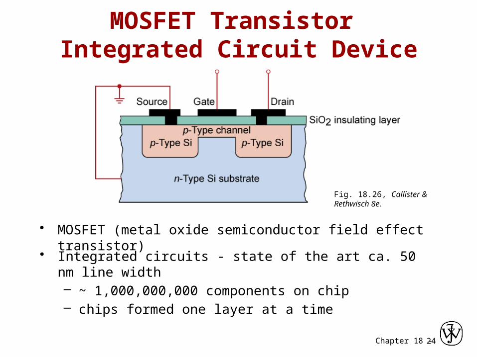
MOSFET Transistor Integrated Circuit Device
• Integrated circuits - state of the art ca. 50 nm line width– ~ 1,000,000,000 components on chip– chips formed one layer at a time
Fig. 18.26, Callister & Rethwisch 8e.
• MOSFET (metal oxide semiconductor field effect transistor)
Chapter 18 -25
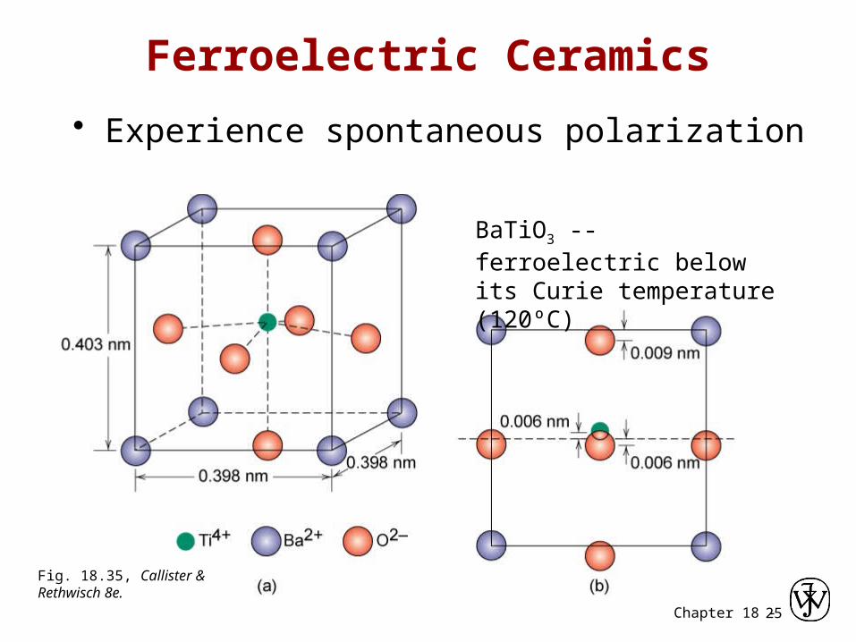
Ferroelectric Ceramics
• Experience spontaneous polarization
Fig. 18.35, Callister & Rethwisch 8e.
BaTiO3 -- ferroelectric below its Curie temperature (120ºC)

Chapter 18 -26
Piezoelectric Materials
stress-free with applied stress
Adapted from Fig. 18.36, Callister & Rethwisch 8e. (Fig. 18.36 from Van Vlack, Lawrence H., Elements of Materials Science and Engineering, 1989, p.482, Adapted by permission of Pearson Education, Inc., Upper Saddle River, New Jersey.)
Piezoelectricity – application of stress induces voltage – application of voltage induces dimensional change

Chapter 18 -27
• Electrical conductivity and resistivity are: -- material parameters -- geometry independent• Conductors, semiconductors, and insulators... -- differ in range of conductivity values -- differ in availability of electron excitation states• For metals, resistivity is increased by -- increasing temperature -- addition of imperfections -- plastic deformation• For pure semiconductors, conductivity is increased by -- increasing temperature -- doping [e.g., adding B to Si (p-type) or P to Si (n-type)]• Other electrical characteristics -- ferroelectricity -- piezoelectricity
Summary

Chapter 18 -28
Core Problems:
Self-help Problems:
ANNOUNCEMENTS
Reading:
Top Related