Chapter 18 - 1 ISSUES TO ADDRESS... How are electrical conductance and resistance characterized ?...
28
Chapter 18 -1 ISSUES TO ADDRESS... How are electrical conductance and resistance characterized? What are the physical phenomena that distinguish conductors, semiconductors, and insulators? For metals, how is conductivity affected by imperfections, temperature, and deformation? For semiconductors, how is conductivity affected by impurities (doping) and temperature? Chapter 18: Electrical Properties
-
Upload
lily-pearson -
Category
Documents
-
view
231 -
download
5
Transcript of Chapter 18 - 1 ISSUES TO ADDRESS... How are electrical conductance and resistance characterized ?...
Chapter 18 - 1
ISSUES TO ADDRESS...
• How are electrical conductance and resistance characterized?
• What are the physical phenomena that distinguish conductors, semiconductors, and insulators?
• For metals, how is conductivity affected by imperfections, temperature, and deformation?
• For semiconductors, how is conductivity affected by impurities (doping) and temperature?
Chapter 18: Electrical Properties

Chapter 18 - 2
• Scanning electron micrographs of an IC:
Fig. (d) from Fig. 12.27(a), Callister & Rethwisch 3e. (Fig. 12.27 is courtesy Nick Gonzales, National Semiconductor Corp., West Jordan, UT.)
• A dot map showing location of Si (a semiconductor): -- Si shows up as light regions.
(b)
View of an Integrated Circuit
0.5 mm
(a)(d)
45 mm
Al
Si (doped)
(d)
• A dot map showing location of Al (a conductor): -- Al shows up as light regions. (c)
Figs. (a), (b), (c) from Fig. 18.27, Callister & Rethwisch 8e.
Chapter 18 - 3
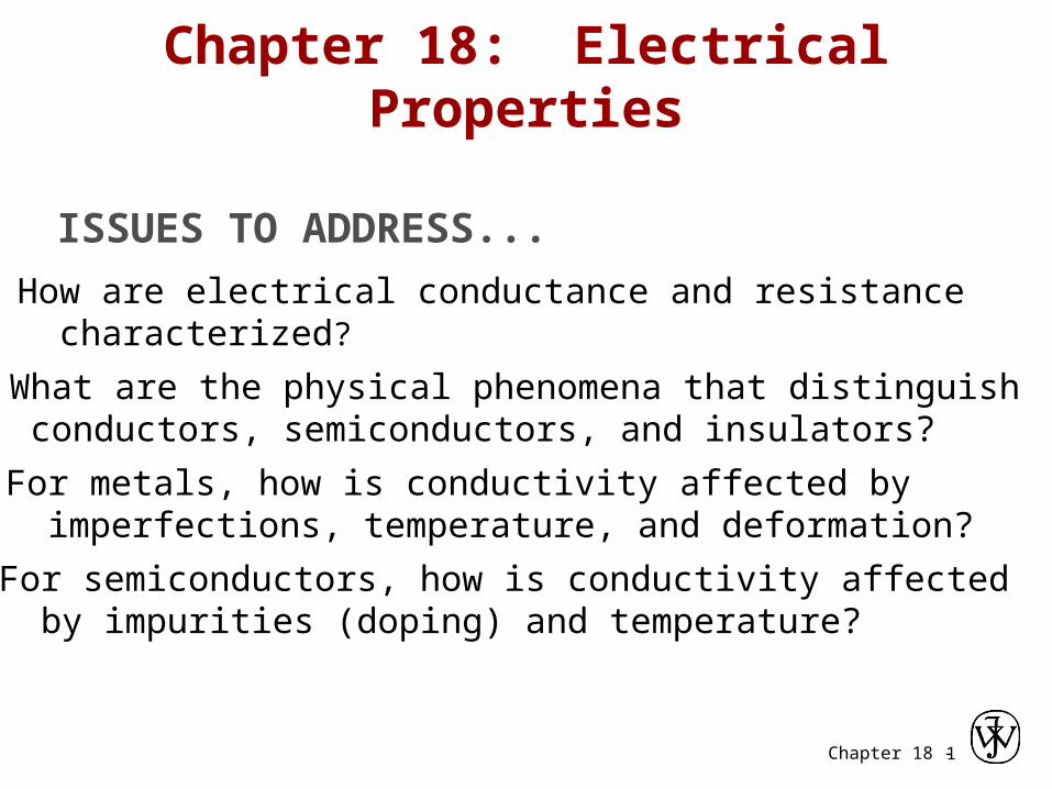
Electrical Conduction• Ohm's Law: V = I R
voltage drop (volts = J/C) C = Coulomb
resistance (Ohms)current (amps = C/s)
1
• Conductivity, s
• Resistivity, r: -- a material property that is independent of sample size and geometry
RA
l
surface area of current flow
current flow path length
Chapter 18 - 4
Electrical Properties
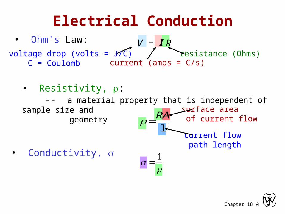
• Which will have the greater resistance?
• Analogous to flow of water in a pipe• Resistance depends on sample geometry and
size.
D
2D
R1 2
D2
2
8D2
2
R2
2D
2
2
D2
R1
8
Chapter 18 - 5
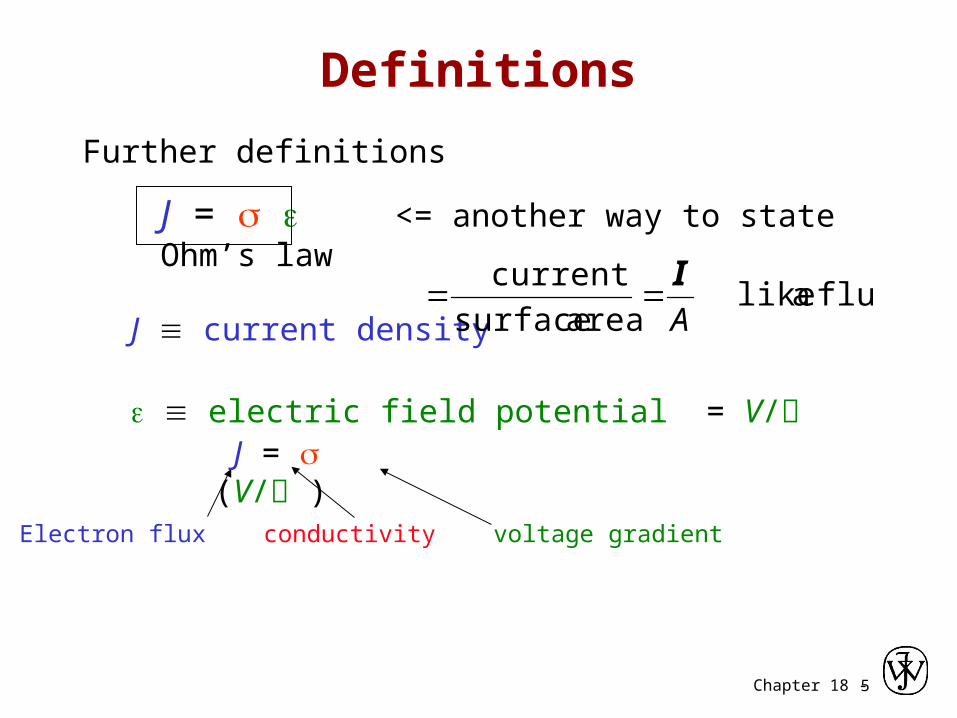
Definitions
Further definitions
J = <= another way to state Ohm’s law
J current density
electric field potential = V/
flux a like area surface
current
A
I
Electron flux conductivity voltage gradient
J = (V/ )

Chapter 18 - 6
• Room temperature values (Ohm-m)-1 = ( - m)-1
Selected values from Tables 18.1, 18.3, and 18.4, Callister & Rethwisch 8e.
Conductivity: Comparison
Silver 6.8 x 10 7
Copper 6.0 x 10 7
Iron 1.0 x 10 7
METALS conductors
Silicon 4 x 10⁻⁴
Germanium 2 x 10 0
GaAs 10 -6
SEMICONDUCTORS
semiconductors
Polystyrene <10-14
Polyethylene 10-15-10-17
Soda-lime glass 10
Concrete 10-9
Aluminum oxide <10-13
CERAMICS
POLYMERS
insulators
-10-10-11
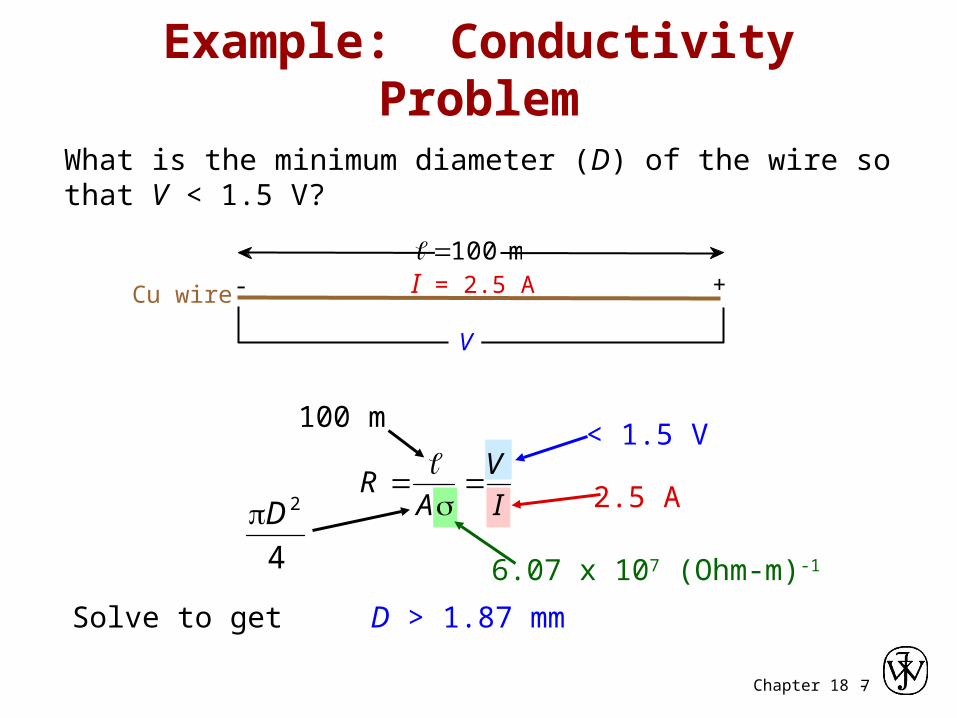
Chapter 18 - 7
What is the minimum diameter (D) of the wire so that V < 1.5 V?
Example: Conductivity Problem
Cu wire I = 2.5 A- +
V
Solve to get D > 1.87 mm
< 1.5 V
2.5 A
6.07 x 10⁷ (Ohm-m)-1
100 m
I
V
AR
4
2D
100 m

Chapter 18 - 8
Electron Energy Band Structures
Adapted from Fig. 18.2, Callister & Rethwisch 8e.
Chapter 18 - 9
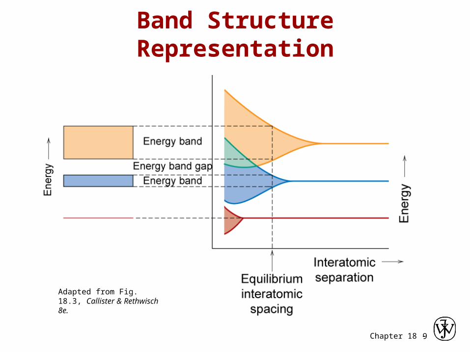
Band Structure Representation
Adapted from Fig. 18.3, Callister & Rethwisch 8e.

Chapter 18 -10
Conduction & Electron Transport• Metals (Conductors):-- for metals empty energy states are adjacent to filled states.
-- two types of band structures for metals
-- thermal energy excites electrons into empty higher energy states.
- partially filled band - empty band that overlaps filled band
filled band
Energy
partly filled band
empty band
GAP
fille
d st
ates
Partially filled band
Energy
filled band
filled band
empty band
fille
d st
ates
Overlapping bands
Chapter 18 -11
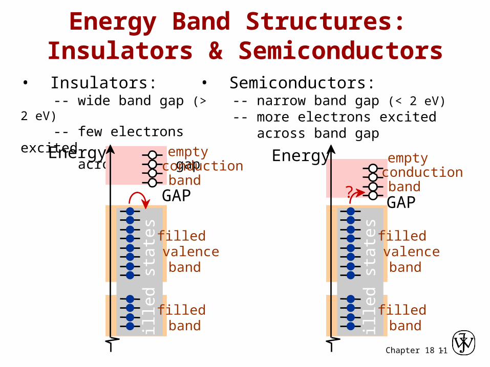
Energy Band Structures: Insulators & Semiconductors
• Insulators: -- wide band gap (> 2 eV) -- few electrons excited across band gap
Energy
filled band
filled valence band
fille
d st
ates
GAP
empty
bandconduction
• Semiconductors: -- narrow band gap (< 2 eV) -- more electrons excited across band gap
Energy
filled band
filled valence band
fille
d st
ates
GAP?
empty
bandconduction
Chapter 18 -12
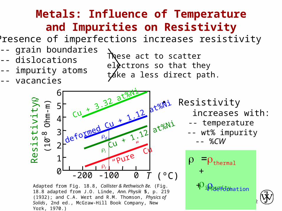
Metals: Influence of Temperature and Impurities on Resistivity
• Presence of imperfections increases resistivity -- grain boundaries -- dislocations -- impurity atoms -- vacancies
These act to scatterelectrons so that theytake a less direct path.
• Resistivity increases with:
=
deformed Cu + 1.12 at%Ni
Adapted from Fig. 18.8, Callister & Rethwisch 8e. (Fig. 18.8 adapted from J.O. Linde, Ann. Physik 5, p. 219 (1932); and C.A. Wert and R.M. Thomson, Physics of Solids, 2nd ed., McGraw-Hill Book Company, New York, 1970.)
T (ºC)-200 -100 0
1
2
3
4
5
6
Res
istiv
ity,
r
(10
-8 O
hm
-m)
0
Cu + 1.12 at%Ni
“Pure” Cu
d -- %CW
+ deformation
i
-- wt% impurity
+ impurity
t
-- temperature
thermal
Cu + 3.32 at%Ni
Chapter 18 -13
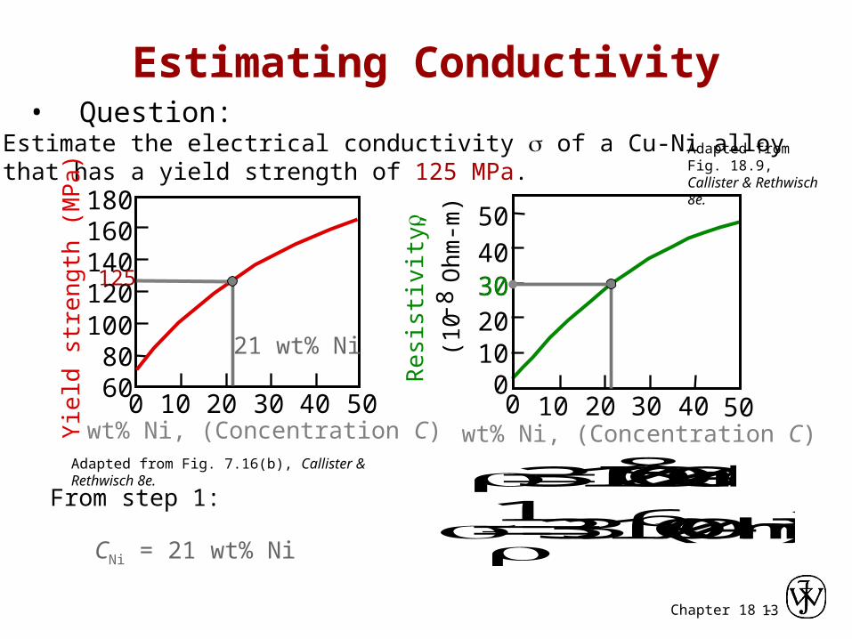
Estimating Conductivity
Adapted from Fig. 7.16(b), Callister & Rethwisch 8e.
• Question:-- Estimate the electrical conductivity of a Cu-Ni alloy that has a yield strength of 125 MPa.
mOhm10 x 30 8
16 )mOhm(10 x 3.31
Yie
ld s
tre
ngt
h (
MP
a)
wt% Ni, (Concentration C)0 10 20 30 40 50
6080
100120140160180
21 wt% Ni
Adapted from Fig. 18.9, Callister & Rethwisch 8e.
wt% Ni, (Concentration C)R
esi
stiv
ity,
r
(10
-8 O
hm
-m)
10 20 30 40 500
10203040
50
0
125
CNi = 21 wt% Ni
From step 1:
30
Chapter 18 -14
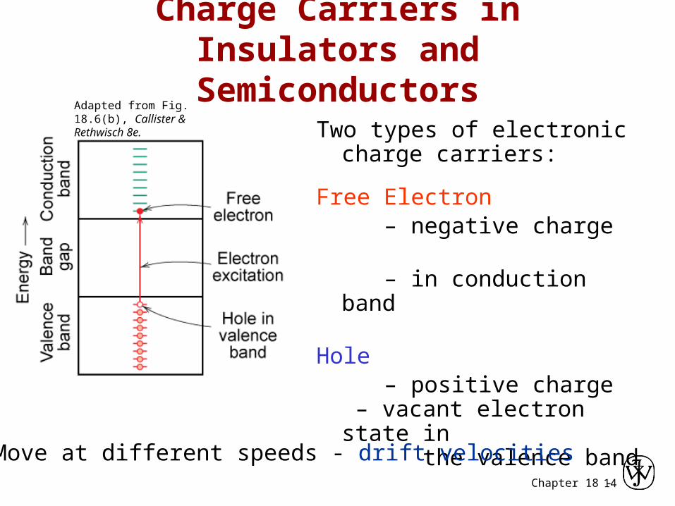
Charge Carriers in Insulators and Semiconductors
Two types of electronic charge carriers:
Free Electron – negative charge – in conduction band
Hole – positive charge
– vacant electron state in the valence band
Adapted from Fig. 18.6(b), Callister & Rethwisch 8e.
Move at different speeds - drift velocities
Chapter 18 -15
Intrinsic Semiconductors
• Pure material semiconductors: e.g., silicon & germanium– Group IVA materials
• Compound semiconductors – III-V compounds
• Ex: GaAs & InSb
– II-VI compounds• Ex: CdS & ZnTe
– The wider the electronegativity difference between the elements the wider the energy gap.
Chapter 18 -16
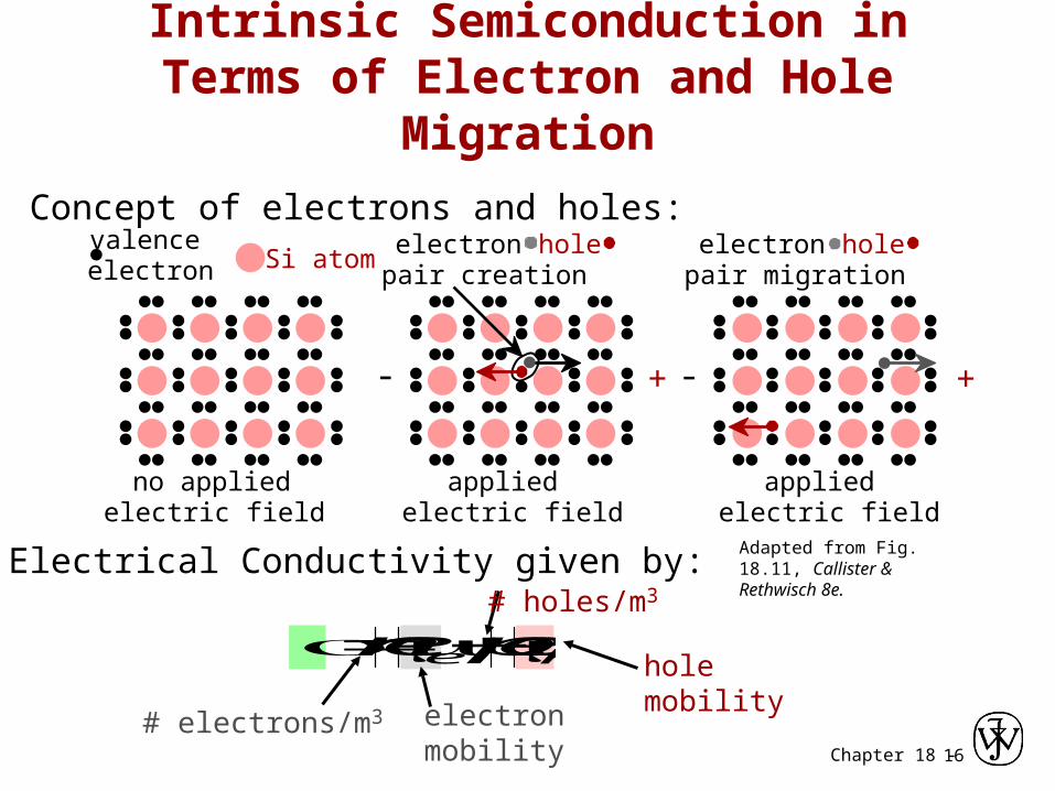
Intrinsic Semiconduction in Terms of Electron and Hole Migration
Adapted from Fig. 18.11, Callister & Rethwisch 8e.
electric field electric field electric field
• Electrical Conductivity given by:
# electrons/m3 electron mobility
# holes/m3
hole mobilityhe epen
• Concept of electrons and holes:
+-
electron hole pair creation
+-
no applied applied
valence electron Si atom
applied
electron hole pair migration
Chapter 18 -17
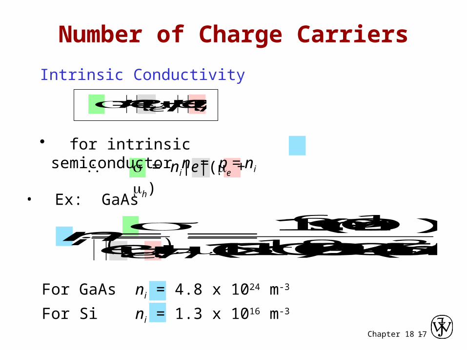
Number of Charge Carriers
Intrinsic Conductivity
)s/Vm 45.085.0)(C10x6.1(
m)(10219
16
hei e
n
For GaAs ni = 4.8 x 1024 m-3
For Si ni = 1.3 x 10¹⁶ m-3
• Ex: GaAs
he epen
• for intrinsic semiconductor n = p = ni = ni|e|(e + h)
Chapter 18 -18
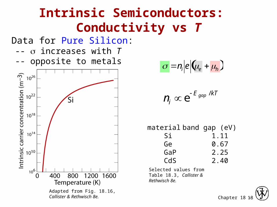
Intrinsic Semiconductors: Conductivity vs T
• Data for Pure Silicon: -- s increases with T -- opposite to metals
Adapted from Fig. 18.16, Callister & Rethwisch 8e.
material Si Ge GaP CdS
band gap (eV) 1.11 0.67 2.25 2.40
Selected values from Table 18.3, Callister & Rethwisch 8e.
ni e Egap / kT
ni e e h
Chapter 18 -19
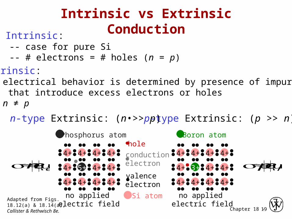
• Intrinsic: -- case for pure Si -- # electrons = # holes (n = p)
• Extrinsic: -- electrical behavior is determined by presence of impurities that introduce excess electrons or holes -- n ≠ p
Intrinsic vs Extrinsic Conduction
3+
• p-type Extrinsic: (p >> n)
no applied electric field
Boron atom
4+ 4+ 4+ 4+
4+
4+4+4+4+
4+ 4+ hep
hole
• n-type Extrinsic: (n >> p)
no applied electric field
5+
4+ 4+ 4+ 4+
4+
4+4+4+4+
4+ 4+
Phosphorus atom
valence electron
Si atom
conductionelectron
een
Adapted from Figs. 18.12(a) & 18.14(a), Callister & Rethwisch 8e.
Chapter 18 -20
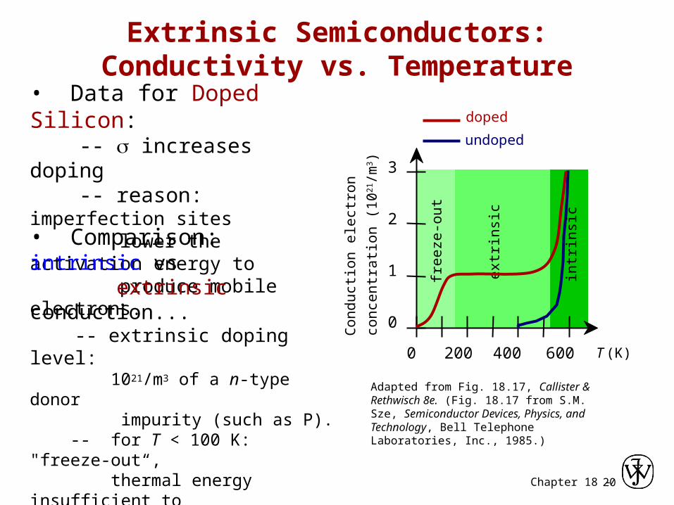
Extrinsic Semiconductors: Conductivity vs. Temperature
• Data for Doped Silicon: -- s increases doping -- reason: imperfection sites lower the activation energy to produce mobile electrons.
• Comparison: intrinsic vs extrinsic conduction... -- extrinsic doping level: 1021/m3 of a n-type donor impurity (such as P). -- for T < 100 K: "freeze-out“, thermal energy insufficient to excite electrons. -- for 150 K < T < 450 K: "extrinsic" -- for T >> 450 K: "intrinsic"
Adapted from Fig. 18.17, Callister & Rethwisch 8e. (Fig. 18.17 from S.M. Sze, Semiconductor Devices, Physics, and Technology, Bell Telephone Laboratories, Inc., 1985.)
Co
nd
uct
ion
ele
ctro
n
con
cen
tra
tion
(1
021/m
3 )T (K)6004002000
0
1
2
3
fre
eze
-ou
t
ext
rin
sic
intr
insi
c
doped
undoped
Chapter 18 -21
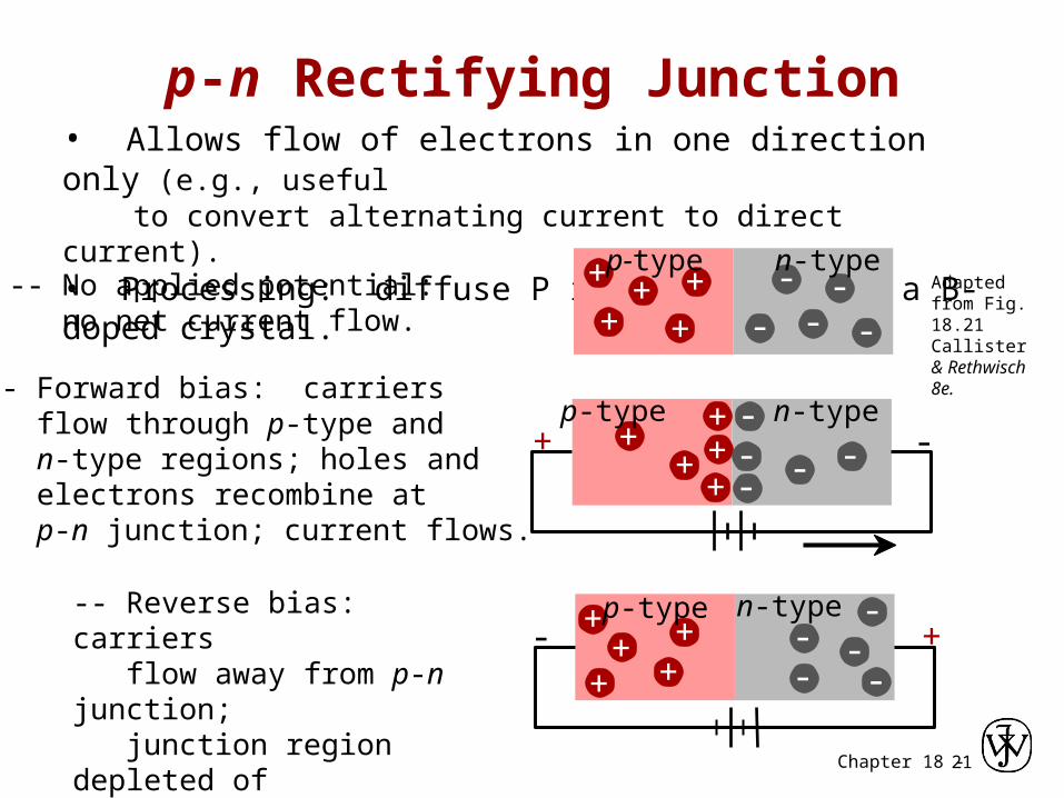
• Allows flow of electrons in one direction only (e.g., useful to convert alternating current to direct current).• Processing: diffuse P into one side of a B-doped crystal.
-- No applied potential: no net current flow.
-- Forward bias: carriers flow through p-type and n-type regions; holes and electrons recombine at p-n junction; current flows.
-- Reverse bias: carriers flow away from p-n junction; junction region depleted of carriers; little current flow.
p-n Rectifying Junction
++
++
+- ---
-p-type n-type
+ -
++ +
++
--
--
-
p-type n-typeAdapted from Fig. 18.21 Callister & Rethwisch 8e.
+++
+
+
---
--
p-type n-type- +
Chapter 18 -22
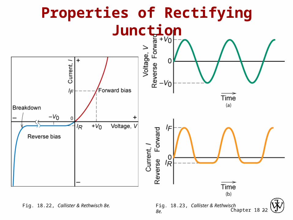
Properties of Rectifying Junction
Fig. 18.22, Callister & Rethwisch 8e. Fig. 18.23, Callister & Rethwisch 8e.

Chapter 18 -23
Junction Transistor
Fig. 18.24, Callister & Rethwisch 8e.
Chapter 18 -24
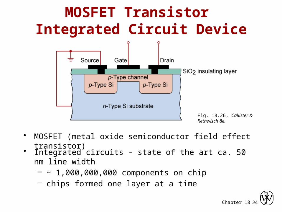
MOSFET Transistor Integrated Circuit Device
• Integrated circuits - state of the art ca. 50 nm line width– ~ 1,000,000,000 components on chip– chips formed one layer at a time
Fig. 18.26, Callister & Rethwisch 8e.
• MOSFET (metal oxide semiconductor field effect transistor)
Chapter 18 -25
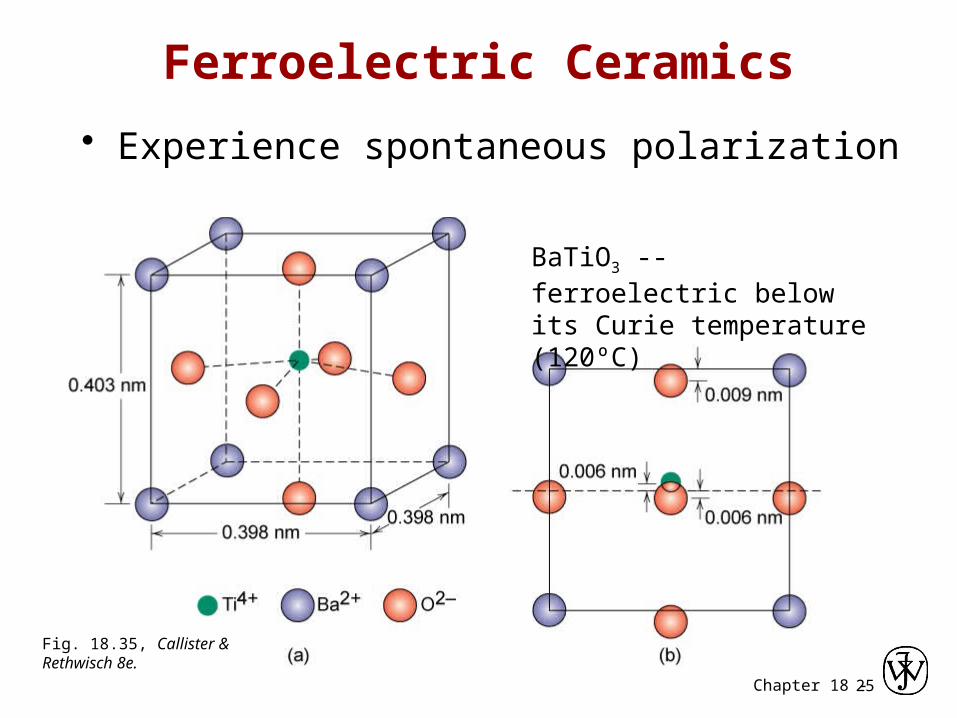
Ferroelectric Ceramics
• Experience spontaneous polarization
Fig. 18.35, Callister & Rethwisch 8e.
BaTiO3 -- ferroelectric below its Curie temperature (120ºC)

Chapter 18 -26
Piezoelectric Materials
stress-free with applied stress
Adapted from Fig. 18.36, Callister & Rethwisch 8e. (Fig. 18.36 from Van Vlack, Lawrence H., Elements of Materials Science and Engineering, 1989, p.482, Adapted by permission of Pearson Education, Inc., Upper Saddle River, New Jersey.)
Piezoelectricity – application of stress induces voltage – application of voltage induces dimensional change

Chapter 18 -27
• Electrical conductivity and resistivity are: -- material parameters -- geometry independent• Conductors, semiconductors, and insulators... -- differ in range of conductivity values -- differ in availability of electron excitation states• For metals, resistivity is increased by -- increasing temperature -- addition of imperfections -- plastic deformation• For pure semiconductors, conductivity is increased by -- increasing temperature -- doping [e.g., adding B to Si (p-type) or P to Si (n-type)]• Other electrical characteristics -- ferroelectricity -- piezoelectricity
Summary

Chapter 18 -28
Core Problems:
Self-help Problems:
ANNOUNCEMENTS
Reading: