ZL38052 Data Sheet - Microsemi
64
1 Microsemi Corporation Confidential and Proprietary Description The ZL38052 is part of Microsemi’s Timberwolf audio processor family of products. These devices feature Microsemi’s innovative AcuEdge acoustic technology, which is a set of highly-complex and integrated algorithms. The Microsemi AcuEdge Technology ZL38052 is designed to provide leading edge far field microphone processing with advanced features targeted for IP and security cameras with high definition (HD) 2-way hands-free voice. The Microsemi AcuEdge Technology license-free, royalty-free intelligent audio Firmware provides Beamforming, Sound Location Estimation, Acoustic Echo Cancellation (AEC), Noise Reduction and a variety of other voice enhancements to improve both the intelligibility and subjective quality of voice in harsh environments. The ZL38052 also incorporates a sound classification feature allowing the system to recognize smoke detector alarms (T3), carbon monoxide detector alarms (T4) and glass break detection. Microsemi offers additional tools to speed up the product development cycle. The MiTuner™ ZLS38508 or ZLS38508LITE GUI software packages allow a user to interactively configure the ZL38052 device. The optional MiTuner ZLE38470BADA Automatic Tuning Kit provides automatic tuning and easy control for manual fine tuning adjustments. Applications • IP Cameras • Security Cameras Typical IP Security Camera Application ZL38052 Microsemi AcuEdge Technology ZLS38052 Firmware There are two Firmware images that may be selected to provide the desired operating mode. Firmware images can be swapped during normal operation to switch modes dynamically. Firmware image size varies with firmware load. ZLS38052.0 (Full Duplex Communication) • Far Field Microphone Processing • Microphone Beamforming • Sound Location Estimation • Full Narrowband and Wideband Acoustic Echo cancellation operation • Supports long tail AEC (up to 256 ms) • Non-Linear AEC provides higher tolerance for speaker distortions • Howling detection/cancellation • Prevents oscillation in AEC audio path • Advanced noise reduction reduces background noise from the near-end speech signal using Psychoacoustic techniques • Various encoding/decoding options:16-bit linear, G.722, G.711 A/μlaw • Send and receive path equalizers ZLS38052.2 (Glass Break and Energy Detectors) • Detects T3 (Temporal smoke alarm) signals • Detects T4 (Temporal carbon monoxide alarm) signals • Detects the sound of breaking glass • Programmable Energy Detector ZL38052 Hardware Features • DSP with Voice Hardware Accelerators Document ID# 154531 Version 1 March 2016 Ordering Information Device OPN Package Packing ZL38052LDF1 64-pin QFN (9x9) Tape & Reel ZL38052LDG1 64-pin QFN (9x9) Tray ZL38052UGB2 56-ball WLCSP (3.1x3.1) Tape & Reel These packages meet RoHS 2 Directive 2011/65/EU of the European Council to minimize the environmental impact of electrical equipment. Timberwolf Digital Signal Processor family, powered by AcuEdge™ Technology Designed for IP Cameras with Sound Classification ZL38052 Preliminary Data Sheet
Transcript of ZL38052 Data Sheet - Microsemi

Document ID# 154531 Version 1 March 2016
Ordering Information Device OPN
Package Packing ZL38052LDF1 64-pin QFN (9x9) Tape & Reel ZL38052LDG1 64-pin QFN (9x9) Tray ZL38052UGB2 56-ball WLCSP (3.1x3.1) Tape & ReelThese packages meet RoHS 2 Directive 2011/65/EU of the European Council
Timberwolf Digital Signal Processor family,powered by AcuEdge™ Technology
Designed for IP Cameras with Sound Classification
ZL38052Preliminary Data Sheet
Description
The ZL38052 is part of Microsemi’s Timberwolf audioprocessor family of products. These devices featureMicrosemi’s innovative AcuEdge acoustic technology,which is a set of highly-complex and integratedalgorithms. The Microsemi AcuEdge TechnologyZL38052 is designed to provide leading edge far fieldmicrophone processing with advanced featurestargeted for IP and security cameras with highdefinition (HD) 2-way hands-free voice.
The Microsemi AcuEdge Technology license-free,royalty-free intelligent audio Firmware providesBeamforming, Sound Location Estimation, AcousticEcho Cancellation (AEC), Noise Reduction and avariety of other voice enhancements to improve boththe intelligibility and subjective quality of voice in harshenvironments. The ZL38052 also incorporates a soundclassification feature allowing the system to recognizesmoke detector alarms (T3), carbon monoxidedetector alarms (T4) and glass break detection.
Microsemi offers additional tools to speed up theproduct development cycle. The MiTuner™ ZLS38508or ZLS38508LITE GUI software packages allow auser to interactively configure the ZL38052 device.The optional MiTuner ZLE38470BADA AutomaticTuning Kit provides automatic tuning and easy controlfor manual fine tuning adjustments.
Applications
• IP Cameras
• Security Cameras
Typical IP Security Camera Application
ZL38052
1
Microsemi Corporation Con
Microsemi AcuEdge Technology ZLS38052 Firmware
There are two Firmware images that may be selectedto provide the desired operating mode. Firmwareimages can be swapped during normal operation toswitch modes dynamically. Firmware image size varieswith firmware load.
ZLS38052.0 (Full Duplex Communication)
• Far Field Microphone Processing
• Microphone Beamforming
• Sound Location Estimation
• Full Narrowband and Wideband Acoustic Echo cancellation operation
• Supports long tail AEC (up to 256 ms)
• Non-Linear AEC provides higher tolerance for speaker distortions
• Howling detection/cancellation
• Prevents oscillation in AEC audio path
• Advanced noise reduction reduces background noise from the near-end speech signal using Psychoacoustic techniques
• Various encoding/decoding options:16-bit linear, G.722, G.711 A/μlaw
• Send and receive path equalizers
ZLS38052.2 (Glass Break and Energy Detectors)
• Detects T3 (Temporal smoke alarm) signals
• Detects T4 (Temporal carbon monoxide alarm) signals
• Detects the sound of breaking glass
• Programmable Energy Detector
ZL38052 Hardware Features
• DSP with Voice Hardware Accelerators
to minimize the environmental impact of electrical equipment.
fidential and Proprietary

Timberwolf Digital Signal Processor family,powered by AcuEdge™ Technology
Designed for IP Cameras with Sound Classification
ZL38052Preliminary Data Sheet
• 2 digital microphone interfaces allowing sampling of up to 4 digital Microphones
• 2 independent headphone drivers
• Dual 16-bit digital-to-analog converters (DACs)
• 16 ohms single-ended or differential drive capability
• 32 mW output drive power into 16 ohms
• 2 Time-Division Multiplexing (TDM) buses
• The ports can be configured for Inter-IC Sound (I2S) or Pulse-Code Modulation (PCM) operation
• PCM operation supports PCM and GCI timing, I2S operation supports I2S and left justified timing
• Each port can be a clock master or a slave
• Each port supports up to four bi-directional streams when configured in PCM mode or two bi-directional streams when configured for I2S mode at data rates from 128 kb/s to 8 Mb/s
• 2 Serial Peripheral Interface (SPI) ports
• The SPI Slave port is recommended as the main communication port with a host processor. The port provides the fastest means to Host Boot and configures the device’s firmware and configuration record.
• The Master SPI port is used to load the device’s firmware and configuration record from external Flash memory (Auto Boot).
• Inter-Integrated Circuit (I2C) Port (pins shared with SPI Slave Port)
• The I2C port can be used as the main communication port with a host processor, and can be used to Host Boot and configure the device’s firmware and configuration record
• General purpose Universal Asynchronous Receiver/Transmitter (UART) port for debug
• The UART port can be used as a debug tool and is used for tuning purposes
• 14 General Purpose Input/Output (GPIO) pins (full operation with Full Duplex Communication Firmware, limited operation with Alarm, Glass Break And Energy Detector Firmware)
• GPIO ports can be used for interrupt and event reporting, fixed function control, bootstrap
2
Microsemi Corporation Con
options, as well as being used for general purpose I/O for communication and controlling external devices
The MiTuner™ Automatic Tuning Kit and ZLS38508 MiTuner GUI
Microsemi's Automatic Tuning Kit option includes:
• Audio Interface Box hardware
• Microphone and Speaker
• ZLS38508 MiTuner GUI software
• Allows tuning of Microsemi's AcuEdge Technology Audio Processor
The ZLS38508 software features:
• Auto Tuning and Subjective Tuning support
• Allows tuning of key parameters of the system design
• Provides visual representations of the audio paths with drop-down menus to program parameters, allowing:
• Control of the audio routing configuration
• Programming of key building blocks in the transmit (Tx) and receive (Rx) audio paths
• Setting analog and digital gains
• Configuration parameters allow users to “fine tune” the overall performance
Tools
• ZLK38000 Evaluation Kit
• MiTuner™ ZLS38508 and ZLS38508LITE GUI
• MiTuner™ ZLE38470BADA Automatic Tuning Kit
fidential and Proprietary
ZL38052 Preliminary Data Sheet
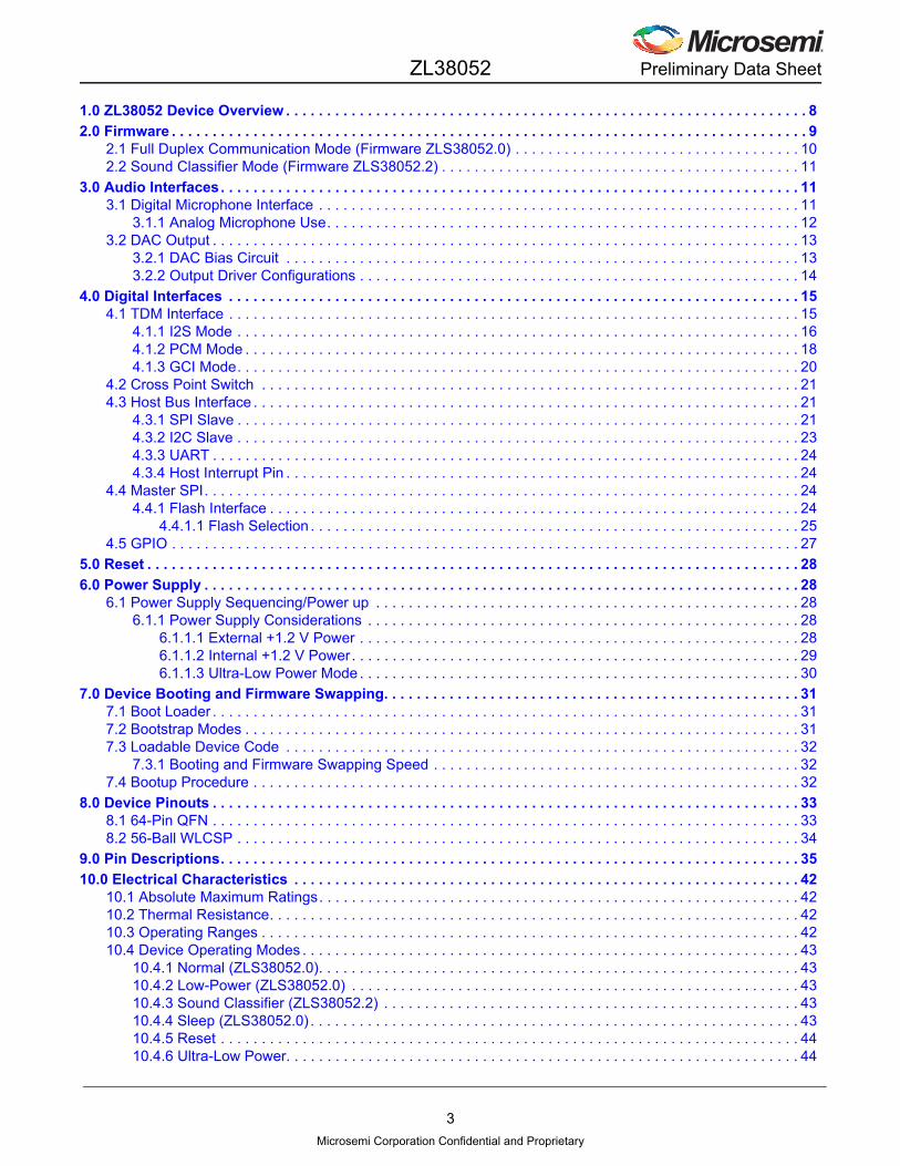
1.0 ZL38052 Device Overview . . . . . . . . . . . . . . . . . . . . . . . . . . . . . . . . . . . . . . . . . . . . . . . . . . . . . . . . . . . . . . . . 8
2.0 Firmware . . . . . . . . . . . . . . . . . . . . . . . . . . . . . . . . . . . . . . . . . . . . . . . . . . . . . . . . . . . . . . . . . . . . . . . . . . . . . . 92.1 Full Duplex Communication Mode (Firmware ZLS38052.0) . . . . . . . . . . . . . . . . . . . . . . . . . . . . . . . . . . . 102.2 Sound Classifier Mode (Firmware ZLS38052.2) . . . . . . . . . . . . . . . . . . . . . . . . . . . . . . . . . . . . . . . . . . . . 11
3.0 Audio Interfaces. . . . . . . . . . . . . . . . . . . . . . . . . . . . . . . . . . . . . . . . . . . . . . . . . . . . . . . . . . . . . . . . . . . . . . . 113.1 Digital Microphone Interface . . . . . . . . . . . . . . . . . . . . . . . . . . . . . . . . . . . . . . . . . . . . . . . . . . . . . . . . . . . 11
3.1.1 Analog Microphone Use. . . . . . . . . . . . . . . . . . . . . . . . . . . . . . . . . . . . . . . . . . . . . . . . . . . . . . . . . . 123.2 DAC Output . . . . . . . . . . . . . . . . . . . . . . . . . . . . . . . . . . . . . . . . . . . . . . . . . . . . . . . . . . . . . . . . . . . . . . . . 13
3.2.1 DAC Bias Circuit . . . . . . . . . . . . . . . . . . . . . . . . . . . . . . . . . . . . . . . . . . . . . . . . . . . . . . . . . . . . . . . 133.2.2 Output Driver Configurations . . . . . . . . . . . . . . . . . . . . . . . . . . . . . . . . . . . . . . . . . . . . . . . . . . . . . . 14
4.0 Digital Interfaces . . . . . . . . . . . . . . . . . . . . . . . . . . . . . . . . . . . . . . . . . . . . . . . . . . . . . . . . . . . . . . . . . . . . . . 154.1 TDM Interface . . . . . . . . . . . . . . . . . . . . . . . . . . . . . . . . . . . . . . . . . . . . . . . . . . . . . . . . . . . . . . . . . . . . . . 15
4.1.1 I2S Mode . . . . . . . . . . . . . . . . . . . . . . . . . . . . . . . . . . . . . . . . . . . . . . . . . . . . . . . . . . . . . . . . . . . . . 164.1.2 PCM Mode . . . . . . . . . . . . . . . . . . . . . . . . . . . . . . . . . . . . . . . . . . . . . . . . . . . . . . . . . . . . . . . . . . . . 184.1.3 GCI Mode. . . . . . . . . . . . . . . . . . . . . . . . . . . . . . . . . . . . . . . . . . . . . . . . . . . . . . . . . . . . . . . . . . . . . 20
4.2 Cross Point Switch . . . . . . . . . . . . . . . . . . . . . . . . . . . . . . . . . . . . . . . . . . . . . . . . . . . . . . . . . . . . . . . . . . 214.3 Host Bus Interface . . . . . . . . . . . . . . . . . . . . . . . . . . . . . . . . . . . . . . . . . . . . . . . . . . . . . . . . . . . . . . . . . . . 21
4.3.1 SPI Slave . . . . . . . . . . . . . . . . . . . . . . . . . . . . . . . . . . . . . . . . . . . . . . . . . . . . . . . . . . . . . . . . . . . . . 214.3.2 I2C Slave . . . . . . . . . . . . . . . . . . . . . . . . . . . . . . . . . . . . . . . . . . . . . . . . . . . . . . . . . . . . . . . . . . . . . 234.3.3 UART . . . . . . . . . . . . . . . . . . . . . . . . . . . . . . . . . . . . . . . . . . . . . . . . . . . . . . . . . . . . . . . . . . . . . . . . 244.3.4 Host Interrupt Pin . . . . . . . . . . . . . . . . . . . . . . . . . . . . . . . . . . . . . . . . . . . . . . . . . . . . . . . . . . . . . . . 24
4.4 Master SPI. . . . . . . . . . . . . . . . . . . . . . . . . . . . . . . . . . . . . . . . . . . . . . . . . . . . . . . . . . . . . . . . . . . . . . . . . 244.4.1 Flash Interface . . . . . . . . . . . . . . . . . . . . . . . . . . . . . . . . . . . . . . . . . . . . . . . . . . . . . . . . . . . . . . . . . 24
4.4.1.1 Flash Selection . . . . . . . . . . . . . . . . . . . . . . . . . . . . . . . . . . . . . . . . . . . . . . . . . . . . . . . . . . . . 254.5 GPIO . . . . . . . . . . . . . . . . . . . . . . . . . . . . . . . . . . . . . . . . . . . . . . . . . . . . . . . . . . . . . . . . . . . . . . . . . . . . . 27
5.0 Reset . . . . . . . . . . . . . . . . . . . . . . . . . . . . . . . . . . . . . . . . . . . . . . . . . . . . . . . . . . . . . . . . . . . . . . . . . . . . . . . . 28
6.0 Power Supply . . . . . . . . . . . . . . . . . . . . . . . . . . . . . . . . . . . . . . . . . . . . . . . . . . . . . . . . . . . . . . . . . . . . . . . . . 286.1 Power Supply Sequencing/Power up . . . . . . . . . . . . . . . . . . . . . . . . . . . . . . . . . . . . . . . . . . . . . . . . . . . . 28
6.1.1 Power Supply Considerations . . . . . . . . . . . . . . . . . . . . . . . . . . . . . . . . . . . . . . . . . . . . . . . . . . . . . 286.1.1.1 External +1.2 V Power . . . . . . . . . . . . . . . . . . . . . . . . . . . . . . . . . . . . . . . . . . . . . . . . . . . . . . 286.1.1.2 Internal +1.2 V Power. . . . . . . . . . . . . . . . . . . . . . . . . . . . . . . . . . . . . . . . . . . . . . . . . . . . . . . 296.1.1.3 Ultra-Low Power Mode . . . . . . . . . . . . . . . . . . . . . . . . . . . . . . . . . . . . . . . . . . . . . . . . . . . . . . 30
7.0 Device Booting and Firmware Swapping. . . . . . . . . . . . . . . . . . . . . . . . . . . . . . . . . . . . . . . . . . . . . . . . . . . 317.1 Boot Loader . . . . . . . . . . . . . . . . . . . . . . . . . . . . . . . . . . . . . . . . . . . . . . . . . . . . . . . . . . . . . . . . . . . . . . . . 317.2 Bootstrap Modes . . . . . . . . . . . . . . . . . . . . . . . . . . . . . . . . . . . . . . . . . . . . . . . . . . . . . . . . . . . . . . . . . . . . 317.3 Loadable Device Code . . . . . . . . . . . . . . . . . . . . . . . . . . . . . . . . . . . . . . . . . . . . . . . . . . . . . . . . . . . . . . . 32
7.3.1 Booting and Firmware Swapping Speed . . . . . . . . . . . . . . . . . . . . . . . . . . . . . . . . . . . . . . . . . . . . . 327.4 Bootup Procedure . . . . . . . . . . . . . . . . . . . . . . . . . . . . . . . . . . . . . . . . . . . . . . . . . . . . . . . . . . . . . . . . . . . 32
8.0 Device Pinouts . . . . . . . . . . . . . . . . . . . . . . . . . . . . . . . . . . . . . . . . . . . . . . . . . . . . . . . . . . . . . . . . . . . . . . . . 338.1 64-Pin QFN . . . . . . . . . . . . . . . . . . . . . . . . . . . . . . . . . . . . . . . . . . . . . . . . . . . . . . . . . . . . . . . . . . . . . . . . 338.2 56-Ball WLCSP . . . . . . . . . . . . . . . . . . . . . . . . . . . . . . . . . . . . . . . . . . . . . . . . . . . . . . . . . . . . . . . . . . . . . 34
9.0 Pin Descriptions. . . . . . . . . . . . . . . . . . . . . . . . . . . . . . . . . . . . . . . . . . . . . . . . . . . . . . . . . . . . . . . . . . . . . . . 35
10.0 Electrical Characteristics . . . . . . . . . . . . . . . . . . . . . . . . . . . . . . . . . . . . . . . . . . . . . . . . . . . . . . . . . . . . . . 4210.1 Absolute Maximum Ratings. . . . . . . . . . . . . . . . . . . . . . . . . . . . . . . . . . . . . . . . . . . . . . . . . . . . . . . . . . . 4210.2 Thermal Resistance. . . . . . . . . . . . . . . . . . . . . . . . . . . . . . . . . . . . . . . . . . . . . . . . . . . . . . . . . . . . . . . . . 4210.3 Operating Ranges . . . . . . . . . . . . . . . . . . . . . . . . . . . . . . . . . . . . . . . . . . . . . . . . . . . . . . . . . . . . . . . . . . 4210.4 Device Operating Modes . . . . . . . . . . . . . . . . . . . . . . . . . . . . . . . . . . . . . . . . . . . . . . . . . . . . . . . . . . . . . 43
10.4.1 Normal (ZLS38052.0). . . . . . . . . . . . . . . . . . . . . . . . . . . . . . . . . . . . . . . . . . . . . . . . . . . . . . . . . . . 4310.4.2 Low-Power (ZLS38052.0) . . . . . . . . . . . . . . . . . . . . . . . . . . . . . . . . . . . . . . . . . . . . . . . . . . . . . . . 4310.4.3 Sound Classifier (ZLS38052.2) . . . . . . . . . . . . . . . . . . . . . . . . . . . . . . . . . . . . . . . . . . . . . . . . . . . 4310.4.4 Sleep (ZLS38052.0) . . . . . . . . . . . . . . . . . . . . . . . . . . . . . . . . . . . . . . . . . . . . . . . . . . . . . . . . . . . . 4310.4.5 Reset . . . . . . . . . . . . . . . . . . . . . . . . . . . . . . . . . . . . . . . . . . . . . . . . . . . . . . . . . . . . . . . . . . . . . . . 4410.4.6 Ultra-Low Power. . . . . . . . . . . . . . . . . . . . . . . . . . . . . . . . . . . . . . . . . . . . . . . . . . . . . . . . . . . . . . . 44
3
Microsemi Corporation Confidential and Proprietary

ZL38052 Preliminary Data Sheet
10.4.7 Current Consumption . . . . . . . . . . . . . . . . . . . . . . . . . . . . . . . . . . . . . . . . . . . . . . . . . . . . . . . . . . . 4510.5 DC Specifications . . . . . . . . . . . . . . . . . . . . . . . . . . . . . . . . . . . . . . . . . . . . . . . . . . . . . . . . . . . . . . . . . . 4610.6 AC Specifications . . . . . . . . . . . . . . . . . . . . . . . . . . . . . . . . . . . . . . . . . . . . . . . . . . . . . . . . . . . . . . . . . . 46
10.6.1 Microphone Interface . . . . . . . . . . . . . . . . . . . . . . . . . . . . . . . . . . . . . . . . . . . . . . . . . . . . . . . . . . . 4610.6.2 DAC. . . . . . . . . . . . . . . . . . . . . . . . . . . . . . . . . . . . . . . . . . . . . . . . . . . . . . . . . . . . . . . . . . . . . . . . 47
10.7 External Clock Requirements . . . . . . . . . . . . . . . . . . . . . . . . . . . . . . . . . . . . . . . . . . . . . . . . . . . . . . . . . 4810.7.1 Crystal Application . . . . . . . . . . . . . . . . . . . . . . . . . . . . . . . . . . . . . . . . . . . . . . . . . . . . . . . . . . . . . 4910.7.2 Clock Oscillator Application . . . . . . . . . . . . . . . . . . . . . . . . . . . . . . . . . . . . . . . . . . . . . . . . . . . . . . 4910.7.3 AC Specifications - External Clocking Requirements . . . . . . . . . . . . . . . . . . . . . . . . . . . . . . . . . . 50
11.0 Timing Characteristics . . . . . . . . . . . . . . . . . . . . . . . . . . . . . . . . . . . . . . . . . . . . . . . . . . . . . . . . . . . . . . . . 5011.1 TDM Interface Timing Parameters . . . . . . . . . . . . . . . . . . . . . . . . . . . . . . . . . . . . . . . . . . . . . . . . . . . . . 51
11.1.1 GCI and PCM Timing Parameters . . . . . . . . . . . . . . . . . . . . . . . . . . . . . . . . . . . . . . . . . . . . . . . . . 5111.1.2 I2S Timing Parameters . . . . . . . . . . . . . . . . . . . . . . . . . . . . . . . . . . . . . . . . . . . . . . . . . . . . . . . . . 54
11.1.2.1 I2S Slave . . . . . . . . . . . . . . . . . . . . . . . . . . . . . . . . . . . . . . . . . . . . . . . . . . . . . . . . . . . . . . . 5411.1.2.2 I2S Master . . . . . . . . . . . . . . . . . . . . . . . . . . . . . . . . . . . . . . . . . . . . . . . . . . . . . . . . . . . . . . 55
11.2 Host Bus Interface Timing Parameters . . . . . . . . . . . . . . . . . . . . . . . . . . . . . . . . . . . . . . . . . . . . . . . . . . 5511.2.1 SPI Slave Port Timing Parameters . . . . . . . . . . . . . . . . . . . . . . . . . . . . . . . . . . . . . . . . . . . . . . . . 5511.2.2 I2C Slave Interface Timing Parameters . . . . . . . . . . . . . . . . . . . . . . . . . . . . . . . . . . . . . . . . . . . . . 57
11.3 UART Timing Parameters . . . . . . . . . . . . . . . . . . . . . . . . . . . . . . . . . . . . . . . . . . . . . . . . . . . . . . . . . . . . 5711.4 Master SPI Timing Parameters . . . . . . . . . . . . . . . . . . . . . . . . . . . . . . . . . . . . . . . . . . . . . . . . . . . . . . . . 58
12.0 AEC Tuning . . . . . . . . . . . . . . . . . . . . . . . . . . . . . . . . . . . . . . . . . . . . . . . . . . . . . . . . . . . . . . . . . . . . . . . . . 59
13.0 Package Outline Drawings . . . . . . . . . . . . . . . . . . . . . . . . . . . . . . . . . . . . . . . . . . . . . . . . . . . . . . . . . . . . . 61
4
Microsemi Corporation Confidential and Proprietary

ZL38052 Preliminary Data Sheet
Figure 1 - IP Camera HD Voice Full Duplex Communication Application . . . . . . . . . . . . . . . . . . . . . . . . . . . . . . . . 9Figure 2 - ZL38052 Audio Processor for IP Cameras . . . . . . . . . . . . . . . . . . . . . . . . . . . . . . . . . . . . . . . . . . . . . . . 9Figure 3 - Single Mono Digital Microphone Interface - Full Duplex Communications Mode or Sound Classification
Mode. . . . . . . . . . . . . . . . . . . . . . . . . . . . . . . . . . . . . . . . . . . . . . . . . . . . . . . . . . . . . . . . . . . . . . . 12Figure 4 - Dual Microphone or Stereo Digital Microphone Interface - Full Duplex Communications Mode . . . . . . 12Figure 5 - Four Digital Microphone Interfaces - Full Duplex Communications Mode. . . . . . . . . . . . . . . . . . . . . . . 12Figure 6 - ECM Circuit . . . . . . . . . . . . . . . . . . . . . . . . . . . . . . . . . . . . . . . . . . . . . . . . . . . . . . . . . . . . . . . . . . . . . . 13Figure 7 - ZL38052 Bias Circuit . . . . . . . . . . . . . . . . . . . . . . . . . . . . . . . . . . . . . . . . . . . . . . . . . . . . . . . . . . . . . . . 14Figure 8 - Audio Output Configurations . . . . . . . . . . . . . . . . . . . . . . . . . . . . . . . . . . . . . . . . . . . . . . . . . . . . . . . . . 15Figure 9 - I2S Mode . . . . . . . . . . . . . . . . . . . . . . . . . . . . . . . . . . . . . . . . . . . . . . . . . . . . . . . . . . . . . . . . . . . . . . . . 17Figure 10 - Left Justified Mode. . . . . . . . . . . . . . . . . . . . . . . . . . . . . . . . . . . . . . . . . . . . . . . . . . . . . . . . . . . . . . . . 17Figure 11 - Dual Codec Configuration . . . . . . . . . . . . . . . . . . . . . . . . . . . . . . . . . . . . . . . . . . . . . . . . . . . . . . . . . . 18Figure 12 - TDM - PCM Slave Functional Timing Diagram (8-bit, xeDX = 0). . . . . . . . . . . . . . . . . . . . . . . . . . . . . 19Figure 13 - TDM - PCM Slave Functional Timing Diagram (8-bit, xeDX = 1). . . . . . . . . . . . . . . . . . . . . . . . . . . . . 19Figure 14 - TDM - PCM Master Functional Timing Diagram (8-bit, xeDX = 0). . . . . . . . . . . . . . . . . . . . . . . . . . . . 19Figure 15 - TDM - PCM Master Functional Timing Diagram (8-bit, xeDX = 1). . . . . . . . . . . . . . . . . . . . . . . . . . . . 20Figure 16 - TDM - GCI Slave Functional Timing Diagram . . . . . . . . . . . . . . . . . . . . . . . . . . . . . . . . . . . . . . . . . . . 20Figure 17 - TDM - GCI Master Functional Timing Diagram . . . . . . . . . . . . . . . . . . . . . . . . . . . . . . . . . . . . . . . . . . 21Figure 18 - SPI Slave Byte Framing Mode - Write . . . . . . . . . . . . . . . . . . . . . . . . . . . . . . . . . . . . . . . . . . . . . . . . . 22Figure 19 - SPI Slave Byte Framing Mode - Read. . . . . . . . . . . . . . . . . . . . . . . . . . . . . . . . . . . . . . . . . . . . . . . . . 22Figure 20 - SPI Slave Word Framing Mode - Write, Multiple Data Words . . . . . . . . . . . . . . . . . . . . . . . . . . . . . . . 22Figure 21 - SPI Slave Word Framing Mode - Read, Multiple Data Words . . . . . . . . . . . . . . . . . . . . . . . . . . . . . . . 23Figure 22 - SPI Slave Command Framing Mode - Write . . . . . . . . . . . . . . . . . . . . . . . . . . . . . . . . . . . . . . . . . . . . 23Figure 23 - SPI Slave Command Framing Mode - Read . . . . . . . . . . . . . . . . . . . . . . . . . . . . . . . . . . . . . . . . . . . . 23Figure 24 - Flash Interface Circuit . . . . . . . . . . . . . . . . . . . . . . . . . . . . . . . . . . . . . . . . . . . . . . . . . . . . . . . . . . . . . 25Figure 25 - External +1.2 V Power Supply Configuration . . . . . . . . . . . . . . . . . . . . . . . . . . . . . . . . . . . . . . . . . . . 29Figure 26 - Internal +1.2 V Power Supply Configuration . . . . . . . . . . . . . . . . . . . . . . . . . . . . . . . . . . . . . . . . . . . . 30Figure 27 - Ultra-Low Power Operation Circuit . . . . . . . . . . . . . . . . . . . . . . . . . . . . . . . . . . . . . . . . . . . . . . . . . . . 31Figure 28 - ZL38052 64-Pin QFN - Top View. . . . . . . . . . . . . . . . . . . . . . . . . . . . . . . . . . . . . . . . . . . . . . . . . . . . . 33Figure 29 - ZL38052 56-Ball WLCSP - Top View. . . . . . . . . . . . . . . . . . . . . . . . . . . . . . . . . . . . . . . . . . . . . . . . . . 34Figure 30 - THD+N Ratio versus Output Power - Driving Low Impedance. . . . . . . . . . . . . . . . . . . . . . . . . . . . . 48Figure 31 - THD+N Ratio versus VRMS - Driving High Impedance. . . . . . . . . . . . . . . . . . . . . . . . . . . . . . . . . . . . 48Figure 32 - Crystal Application Circuit . . . . . . . . . . . . . . . . . . . . . . . . . . . . . . . . . . . . . . . . . . . . . . . . . . . . . . . . . . 49Figure 33 - Clock Oscillator Application Circuit . . . . . . . . . . . . . . . . . . . . . . . . . . . . . . . . . . . . . . . . . . . . . . . . . . . 49Figure 34 - Timing Parameter Measurement Digital Voltage Levels . . . . . . . . . . . . . . . . . . . . . . . . . . . . . . . . . . . 50Figure 35 - GCI Timing, 8-bit . . . . . . . . . . . . . . . . . . . . . . . . . . . . . . . . . . . . . . . . . . . . . . . . . . . . . . . . . . . . . . . . . 52Figure 36 - PCM Timing, 8-bit with xeDX = 0 (Transmit on Negative PCLK Edge) . . . . . . . . . . . . . . . . . . . . . . . . 52Figure 37 - PCM Timing, 8-bit with xeDX = 1 (Transmit on Positive PCLK Edge) . . . . . . . . . . . . . . . . . . . . . . . . . 53Figure 38 - Slave I2S Timing . . . . . . . . . . . . . . . . . . . . . . . . . . . . . . . . . . . . . . . . . . . . . . . . . . . . . . . . . . . . . . . . . 54Figure 39 - Master I2S Timing . . . . . . . . . . . . . . . . . . . . . . . . . . . . . . . . . . . . . . . . . . . . . . . . . . . . . . . . . . . . . . . . 55Figure 40 - SPI Slave Timing . . . . . . . . . . . . . . . . . . . . . . . . . . . . . . . . . . . . . . . . . . . . . . . . . . . . . . . . . . . . . . . . . 56Figure 41 - I2C Timing Parameter Definitions . . . . . . . . . . . . . . . . . . . . . . . . . . . . . . . . . . . . . . . . . . . . . . . . . . . . 57Figure 42 - UART_RX Timing . . . . . . . . . . . . . . . . . . . . . . . . . . . . . . . . . . . . . . . . . . . . . . . . . . . . . . . . . . . . . . . . 58Figure 43 - UART_TX Timing. . . . . . . . . . . . . . . . . . . . . . . . . . . . . . . . . . . . . . . . . . . . . . . . . . . . . . . . . . . . . . . . . 58Figure 44 - Master SPI Timing . . . . . . . . . . . . . . . . . . . . . . . . . . . . . . . . . . . . . . . . . . . . . . . . . . . . . . . . . . . . . . . . 59Figure 45 - AIB System Board Connection . . . . . . . . . . . . . . . . . . . . . . . . . . . . . . . . . . . . . . . . . . . . . . . . . . . . . . 60Figure 46 - 64-Pin QFN . . . . . . . . . . . . . . . . . . . . . . . . . . . . . . . . . . . . . . . . . . . . . . . . . . . . . . . . . . . . . . . . . . . . . 61Figure 47 - Recommended 64-Pin QFN Land Pattern - Top View . . . . . . . . . . . . . . . . . . . . . . . . . . . . . . . . . . . . . 62Figure 48 - 56-Ball WLCSP . . . . . . . . . . . . . . . . . . . . . . . . . . . . . . . . . . . . . . . . . . . . . . . . . . . . . . . . . . . . . . . . . . 63
5
© 2015 Microsemi Corporation. All Rights Reserved.

ZL38052 Preliminary Data Sheet
6
Microsemi Corporation Confidential and Proprietary

ZL38052 Preliminary Data Sheet
7
Microsemi Corporation Confidential and Proprietary
Table 1 - Allowable TDM Configurations. . . . . . . . . . . . . . . . . . . . . . . . . . . . . . . . . . . . . . . . . . . . . . . . . . . . . . . . 16Table 2 - HBI Slave Interface Selection . . . . . . . . . . . . . . . . . . . . . . . . . . . . . . . . . . . . . . . . . . . . . . . . . . . . . . . . . 21Table 3 - Flash Devices Tested with the ZL38052 . . . . . . . . . . . . . . . . . . . . . . . . . . . . . . . . . . . . . . . . . . . . . . . . . 26Table 4 - Supported Flash Types . . . . . . . . . . . . . . . . . . . . . . . . . . . . . . . . . . . . . . . . . . . . . . . . . . . . . . . . . . . . . . 27Table 5 - Q1 Component Options . . . . . . . . . . . . . . . . . . . . . . . . . . . . . . . . . . . . . . . . . . . . . . . . . . . . . . . . . . . . . 30Table 6 - Bootstrap Modes . . . . . . . . . . . . . . . . . . . . . . . . . . . . . . . . . . . . . . . . . . . . . . . . . . . . . . . . . . . . . . . . . . . 31Table 7 - Reset Pin Description . . . . . . . . . . . . . . . . . . . . . . . . . . . . . . . . . . . . . . . . . . . . . . . . . . . . . . . . . . . . . . . 35Table 8 - DAC Pin Descriptions . . . . . . . . . . . . . . . . . . . . . . . . . . . . . . . . . . . . . . . . . . . . . . . . . . . . . . . . . . . . . . . 35Table 9 - Microphone Pin Descriptions . . . . . . . . . . . . . . . . . . . . . . . . . . . . . . . . . . . . . . . . . . . . . . . . . . . . . . . . . 35Table 10 - TDM and I2S Ports Pin Descriptions. . . . . . . . . . . . . . . . . . . . . . . . . . . . . . . . . . . . . . . . . . . . . . . . . . . 35Table 11 - HBI - SPI Slave Port Pin Descriptions . . . . . . . . . . . . . . . . . . . . . . . . . . . . . . . . . . . . . . . . . . . . . . . . . . 38Table 12 - Master SPI Port Pin Descriptions . . . . . . . . . . . . . . . . . . . . . . . . . . . . . . . . . . . . . . . . . . . . . . . . . . . . . 38Table 13 - UART Pin Descriptions. . . . . . . . . . . . . . . . . . . . . . . . . . . . . . . . . . . . . . . . . . . . . . . . . . . . . . . . . . . . . 39Table 14 - GPIO Pin Descriptions . . . . . . . . . . . . . . . . . . . . . . . . . . . . . . . . . . . . . . . . . . . . . . . . . . . . . . . . . . . . . 39Table 15 - Oscillator Pin Descriptions . . . . . . . . . . . . . . . . . . . . . . . . . . . . . . . . . . . . . . . . . . . . . . . . . . . . . . . . . . 40Table 16 - Supply and Ground Pin Descriptions . . . . . . . . . . . . . . . . . . . . . . . . . . . . . . . . . . . . . . . . . . . . . . . . . . 41Table 17 - No Connect Pin Description . . . . . . . . . . . . . . . . . . . . . . . . . . . . . . . . . . . . . . . . . . . . . . . . . . . . . . . . . 41
ZL38052 Preliminary Data Sheet
1.0 ZL38052 Device Overview
The Microsemi ZL38052 Audio Processor powered by ZLS38052 AcuEdge™ Technology Firmware is ideal for providing high definition audio to IP cameras. The ZL38052 has two primary modes of operation 1) Full Duplex Communication mode and 2) Sound Classifier mode.
In general, the two modes of operation provide the following functionality:
Full Duplex Communication Mode
This mode offers a high performance two way audio solution offering the following features:
• Wide band (16 kHz sampling) operation
• Configurable Acoustic Echo Canceler (AEC)
• Programmable echo cancellation tail length up to 256 ms
• Non-linear Acoustic Echo Controller
• Non-Linear Processor (NLP)
• Beamforming with two or three microphone array
• Sound Locator identifies the direction of the loudest audio source, providing alerts of potential interest
• Patented Psycho-Acoustic Noise Reduction – up to 20 dB for white noise
• Integrated Compressor / Limiter / Expander enhances intelligible speech from significant distances
• Patented Anti-Howling – reduces oscillation in echo canceller audio path, including co-located devices
• Parametric Equalizers in the Send and Receive paths
• Programmable Tone Generators to generate DTMF, tone ringer, and test tones
• Cross Point Switch provides signal mixing
• Programmable coding (/A-law ITU-T G.711, G.722, or 16- bit linear) at line interface
Sound Classifier Mode
The mode offers a sound classification feature with the following features:
• Smoke detector alarm (T3)
• Carbon monoxide alarms (T4)
• Glass break detector
• Programmable Energy Detector
A typical IP Camera application is presented in Figure 1.
8
Microsemi Corporation Confidential and Proprietary

ZL38052 Preliminary Data Sheet
Figure 1 - IP Camera HD Voice Full Duplex Communication Application
The main functional blocks of the ZL38052 device are shown in Figure 2.
Figure 2 - ZL38052 Audio Processor for IP Cameras
2.0 Firmware
The two modes of operation in the ZL38052 (Full Duplex Communication and Sound Classification) are selecteddepending on which Firmware is loaded into the device. The Firmware is initially loaded at power up, either fromexternal serial Flash or from a host controller (see 7.0, “Device Booting and Firmware Swapping“ on page 31). Realtime switching between the two Firmware modes can be done during normal operation, however this requires ahost controller to support. There are timing constraints that should be noted for Firmware Swapping (see 11.2,“Host Bus Interface Timing Parameters“ on page 55 for more information).
ZL38052
Flash(optional)
Host/IPProcessor
Ethernet
SPI/I2C
TDM/I2S
Speaker
SPIM
DAC1_P
DAC1_M
OptionalSpeakerDriver
Digital Microphones
DMIC_IN1DMIC_CLK
64-pin QFN
9
Microsemi Corporation Confidential and Proprietary
ZL38052 Preliminary Data Sheet
The ZL38052 Firmware Manual provides detailed information on the use of the two firmware modes of operation forthe ZL38052 and should be consulted.
The majority of the signal processing (AEC, Equalization, Noise Reduction, Beamforming, CLE, etc.) runs in theAudio Processor Block at 16 kHz. Each of the audio inputs (Digital Mics, I2S/TDM) and outputs (DACs, I2S/TDM)can be routed amongst themselves or to the Audio Processor via a highly configurable Cross Point Switch.
The ZL38052 device provides the following peripheral interfaces:
• 2 digital microphone interfaces allowing sampling of up to 4 digital microphones
• 2 Time-Division Multiplexing (TDM) buses
• The ports can be configured for Inter-IC Sound (I2S) or Pulse-Code Modulation (PCM) operation
• PCM operation supports PCM and GCI timing, I2S operation supports I2S and left justified timing
• Each port can be a clock master or a slave
• Each port supports up to four bi-directional streams when configured in PCM mode or two bi-directional streams when configured for I2S mode at data rates from 128 kb/s to 8 Mb/s
• Sample rate conversions are automatically done when data is sent/received at different rates than is processed internally
• SPI – The device provides two Serial Peripheral Interface (SPI) ports
• The SPI Slave port is recommended as the main communication port with a host processor. The port provides the fastest means to Host Boot and configure the device’s firmware and configuration record*.
• The Master SPI port is used to loads the device’s firmware and configuration record from external Flash memory (Auto Boot).
• I2C - The device provides one Inter-Integrated Circuit (I2C) port. (pins are shared with the SPI Slave port)
• The I2C port can be used as the main communication port with a host processor, and can be used to Host Boot and configure the device’s firmware and configuration record.
• UART – The device provides one Universal Asynchronous Receiver/Transmitter (UART) port
• The UART port can be used as a debug tool and is used for tuning purposes.
• GPIO – The device provides 14 General Purpose Input/Output (GPIO) ports (full operation with Full Duplex Communication Firmware, limited operation with Alarm, Glass Break And Energy Detector Firmware).
• GPIO ports can be used for interrupt and event reporting, fixed function control, bootstrap options, as well as being used for general purpose I/O for communication and controlling external devices.
• The 56 pin WLCSP package is limited to 11 GPIOs.
* Note: The configuration record is a set of register values that are customizable by the application developer toconfigure and tune the ZL38052 for a particular design. Refer to the Microsemi AcuEdge™ Technology ZLS38052Firmware Manual for firmware and configuration record information.
2.1 Full Duplex Communication Mode (Firmware ZLS38052.0)
The ZLS38052.0 Firmware offers a sophisticated audio compressor/limiter/expander (CLE) with adjustable attackand decay time. This feature along with Beamforming and advanced Noise Reduction allows for Far FieldMicrophone pick-up.
The full duplex communication firmware (ZLS38052.0) supports the following additional ports:
• 2 independent headphone drivers
• Dual 16-bit digital-to-analog converters (DACs)
• 16 ohms single-ended or differential drive capability
10
Microsemi Corporation Confidential and Proprietary

ZL38052 Preliminary Data Sheet
• 32 mW output drive power into 16 ohms
2.2 Sound Classifier Mode (Firmware ZLS38052.2)
This mode of operation uses a single microphone input to be able to provide enhanced Sound Classification. Thismode of operation supports:
• Detects T3 (temporal smoke alarm) signals
• Detects T4 (temporal carbon monoxide alarm) signals
• Detects the sound of breaking glass
• Programmable Energy Detector
Refer to the Microsemi AcuEdge™ Technology ZLS38052 Firmware Manual for more information on the Firmwareoptions and usage for the ZL38052.
3.0 Audio Interfaces
3.1 Digital Microphone Interface
The ZL38052 supports up to four digital microphones using the DMIC_CLK, DMIC_IN1, and DMIC_IN2 interfacepins.
The ZL38052 digital microphone clock output (DMIC_CLK) is either 1.024 MHz or 3.072 MHz depending on theselected TDM-A sample rate. Selecting 16 kHz TDM-A sample rate corresponds to a 1.024 MHz digital microphoneclock and selecting a 48 kHz sample rate corresponds to a 3.072 MHz digital microphone clock. Microphone data isdecimated and filtered to operate at 16 kHz sampling rate of the Audio Processing block. When there is no TDM-Abus to set the sample rate, the ZL38052 will operate from the crystal (or clock oscillator) and will pass digital audiofrom the microphones operating at a 48 kHz sampling rate.
When in full duplex communication mode, AEC can be performed on up to three microphones selected to go to theZL38052 voice processing section, the other paths may be routed to the TDM bus for use by the host or an externalCodec. Alternatively the host processor can switch different microphones to the voice processing inputs. Note thatwhen in sound classification mode, only one microphone is used/required. It runs at 1.024 MHz sampling rate.
A stereo digital microphone, or two separate mono digital microphones, can send two microphone channels on onepin by sending the data for one channel on the rising edge and one channel on the falling edge. The selection forwhich clock edge is used to clock in the microphone data (rising/falling) is done via the Microphone EnableConfiguration register (host writable over the HBI) or in the configuration record (loaded from Flash). Various digitalmicrophone interfaces are presented in Figures 3 - 5.
An electret condenser microphone can be used with the digital microphone input by using a Digital ElectretMicrophone Pre-Amplifier device as shown in Figure 6.
Beamforming can be performed with 2 or 3 microphones. The Beamformer uses the signals from multiplemicrophones to determine the direction of arrival of various sound sources. The Beamformer accepts thosesources that it determines are in the direction of interest and attenuates those that are deemed to be coming fromother directions. By attenuating anything outside of the beam, the distance of microphone pick-up improves andinterfering sounds are reduced. The Beamformer’s beam width, steering angle, and out-of-beam attenuation areprogrammable. The physical spacing between microphones is important when implementing Beamforming.Beamforming with two microphones is most optimal when the microphones are spaced 50mm to 60mm apart.When using three microphones, the optimal spacing is 30mm apart. The microphones must also be oriented alongthe same plane and face the same direction. Please consult with Microsemi applications support for moreinformation when optimizing the design for Beamforming.
In addition to Beamforming, the Microsemi AcuEdge™ Technology Sound Location feature reports the angle atwhich a sound arrives at the microphone array (2 or 3 microphones).
11
Microsemi Corporation Confidential and Proprietary

ZL38052 Preliminary Data Sheet
Figure 3 - Single Mono Digital Microphone Interface Full Duplex Communications Mode or Sound Classification Mode
Figure 4 - Dual Microphone or Stereo Digital Microphone Interface Full Duplex Communications Mode
Figure 5 - Four Digital Microphone Interfaces Full Duplex Communications Mode
3.1.1 Analog Microphone Use
To use analog electret condenser microphones (ECM) with the digital microphone interface, a Digital ElectretMicrophone Pre-Amplifier device is required. Figure 6 illustrates an analog microphone connection.
ZL38052
Digital Microphone
DMIC_CLK
DMIC_IN1
CLK
DATA
L/R SEL
ZL38052
Digital Microphones
Left
RightDMIC_CLK
DMIC_IN1
CLK
DATA
CLK
DATA
CLK
DATADMIC_IN2
L/R SEL
L/R SEL
L/R SEL
CLK
DATA
L/R SEL
Right
Left
ZL38052
Stereo Digital Microphone
Left
RightDMIC_CLK
DMIC_IN1
CLK
DATA
CLK
DATA
L/R SEL
L/R SEL
12
Microsemi Corporation Confidential and Proprietary

ZL38052 Preliminary Data Sheet
The analog microphone is wired to an optional differential amplifier which amplifies and converts the microphonesignal to single-ended. The microphone signals are then further amplified and digitized through the Digital ElectretMicrophone Pre-Amplifiers and applied to the ZL38052 digital microphone input. A Microsemi AAP149B ECM Pre-Amplifier is shown.
The ZL38052 provides the clock to activate the Digital Electret Microphone Pre-Amplifier.
Figure 6 - ECM Circuit
When using an analog microphone, operation in Low-Power mode is not recommended. For more information, see10.4, “Device Operating Modes“ on page 43.
3.2 DAC Output
The ZL38052 has two 16-bit fully differential delta-sigma digital-to-analog converters. The two output DACsindependently drive an analog output subsystem. Each subsystem is able to drive two output pins, representingfour independent single-ended headphone outputs that can be driven by two independent data streams. The pinscan be independently configured. Four analog gains on each headphone output are provided and can be set to:1x, 0.5x, 0.333x, or 0.25x.
Note: Only the positive DAC outputs are available with the 56-ball WLCSP package. The 56-ball WLCSP package provides two independent single-ended headphone outputs that can be driven by two independent data streams.
The headphone amplifiers are self-protecting so that a direct short from the output to ground or a direct short acrossthe terminals does not damage the device.
The ZL38052 provides audible pop suppression which reduces pop noise in the headphone earpiece when thedevice is powered on/off or when the device channel configurations are changed. This is especially important whendriving a headphone single-ended through an external capacitor (see 3.2.2, “Output Driver Configurations“,configuration C).
The DACs and headphone amplifiers can be powered down if they are not required for a given application. To fullypower down the DACs, disable both the positive and negative outputs.
3.2.1 DAC Bias Circuit
The common mode bias voltage output signal (CREF) for the DAC output buffers must be decoupled through a0.1 F (CREF1) and a 1.0 F (CREF2) ceramic capacitor to VSS. The positive DAC reference voltage output (CDAC)must be decoupled through a 0.1 F (CDAC) ceramic capacitor to VSS as shown in Figure 7.
All capacitors can have a 20% tolerance and should have a minimum voltage rating of 6.3 V.
ZL38052
ECMDMIC_CLK
DMIC_IN1
ECMpreamp
Vbias VDD
CLK
DATA
DGND
IN
VDD
‐
+ L/RSelect
Optional circuitryCommonly used for handset microphone with long cord
DGNDAGNDAGND
AAP149B
13
Microsemi Corporation Confidential and Proprietary

ZL38052 Preliminary Data Sheet
Figure 7 - ZL38052 Bias Circuit
3.2.2 Output Driver Configurations
Figure 8 shows the different possible output driver configurations for the 64-pin QFN package. When using the 56-ball WLCSP package, only the positive outputs DAC1_P and DAC2_P are provided.
The two output DACs independently drive positive and negative headphone driver amplifiers. The output pins canbe independently configured in the following ways:
A. 64-pin QFN Direct differential drive of a speaker as low as 32 ohms. For this configuration an analog gain of 1xis commonly used. (Differentially driving a 16 ohm speaker is possible, but only with the same amount of power asin the single-ended case. The signal level must be reduced to not exceed ½ scale in this case.)
B. 64-pin QFN Direct differential drive of a high impedance power amplifier. A Class D amplifier is recommended for this speaker driver. Use an ON Semiconductor® NCP2820 or equivalent. A 1 F coupling capacitor is generally used with the Class D amplifier. The analog gain setting depends on the gain of the Class D amplifier, analog gain settings of 0.25x or 0.5x are commonly used.
C. Both packages Driving either a high impedance or a capacitively coupled speaker as low as 16 ohms single-ended. For this configuration an analog gain of 1x is commonly used. The coupling capacitor value can vary from10 f to 100 f depending on the type of earpiece used and the frequency response desired.
ZL38052
CREF
CDAC
CREF1
CREF2
CDAC
0.1 uF
0.1 uF
1.0 uF
14
Microsemi Corporation Confidential and Proprietary

ZL38052 Preliminary Data Sheet
Figure 8 - Audio Output Configurations
4.0 Digital Interfaces
4.1 TDM Interface
The ZL38052 device has two generic TDM interfaces, TDM-A and TDM-B. Each interface consists of four signals:
• Data clock (PCLK/I2S_SCK)
• Data rate sync (FS/I2S_WS)
• Serial data input (DR/I2S_SDI)
• Serial data output (DX/I2S_SDO)
The TDM ports can be configured for Inter-IC Sound (I2S) or Pulse-Code Modulation (PCM) operation.
Each TDM block is capable of being a master or a slave, however both highways must be synchronous to eachother (derived from a common clock domain).
Operation of the TDM interfaces are subject to the following limitations.
ZL38052
64-pin QFN
+
-
+
-
En 1P
En 1M
DAC 1 +-
DAC1_M
DAC1_P
A BC
+-
+
-
+
-
+
-
En 2P
En 2M
DAC 1 +-
DAC2_M
DAC2_P
A BC
+-
+
-
15
Microsemi Corporation Confidential and Proprietary
ZL38052 Preliminary Data Sheet
Table 1 - Allowable TDM Configurations
Note 1: When TDM-A is a slave, then the device can be run without a crystal. However, this mode requires that the PCLKA and FSA signals are always present and PCLKA must be an integer multiple of 2.048 MHz. For crystal-less operation at power-on, PCLKA will be auto-detected with only 8 kHz and 16 kHz frame syncs being allowed.
Note 2: This combination requires that both TDM-A clock and TDM-B clock be physically connected to the same source.
Note 3: The Audio Processing block accepts these sample rates but the Audio Processing block always runs at a 16 kHz sampling rate.
While a TDM bus configuration may carry many encoded audio streams, the ZL38052 device can only address amaximum of 4 bi-directional audio streams per TDM bus. These four audio streams are referred to as channels #1through #4, and each of these channels can be independently configured to decode any of the TDM bus’s audiostreams.
For a given TDM bus, once it is configured for a data sample rate and encoding, all data rates and encoding on thatbus will be the same. 16-bit linear data will be sent on consecutive 8-bit timeslots (e.g., if timeslot N is programmedin the timeslot registers, the consecutive timeslot is N+1).
The TDM interface supports bit reversal (LSB first MSB first) and loopbacks within the TDM interface andfrom one interface to another (see “Cross Point Switch” on page 21).
The generic TDM interface supports the following mode and timing options.
4.1.1 I2S Mode
In I2S mode, the 4-wire TDM port conforms to the I2S protocol and the port pins become I2S_SCK, I2S_WS,I2S_SDI, and I2S_SDO (refer to Table 10 for pin definitions). Both TDM buses have I2S capability.
An I2S bus supports two bi-directional data streams, left and right channel, by using the send and receive data pinsutilizing the common clock and word signals. The send data is transmitted on the I2S_SDO line and the receivedata is received on the I2S_SDI line.
The I2S port can be used to connect external analog-to-digital converters or Codecs. The port can operate inmaster mode where the ZL38052 is the source of the port clocks, or slave mode where the word select and serialclocks are inputs to the ZL38052.
The word select (I2S_WS) defines the I2S data rate and sets the frame period when data is transmitted for the leftand right channels. A frame consists of one left and one right audio channel. The I2S ports operate at 8, 16, and48 kHz data rates as a slave or master (as specified in Table 1). Per the I2S standard, the word select is outputusing a 50% duty cycle.
The serial clock (I2S_SCK) rate sets the number of bits per word select frame period and defines the frequency ofI2S_CLK. I2S data is input and output at the serial clock rate. Input data bits are received on I2S_SDI and outputdata bits are transmitted on I2S_SDO. Data bits are always MSB first. The number of clock and data bits per framecan be programmed as 8, 16, 32, 64, 96, 128, 192, 256, 384, 512, or 1024. Any input data bits that are receivedafter the LSB are ignored.
TDM-A Mode TDM-B ModeSupported
Sample Rates3 (kHz)
Requirements / Limitations
Master Master8, 16, 48
Both TDM-A and TDM-B must be configured for the same data clock and data sync.
Master Slave-SynchronousThe TDM-B sync rate must either be the same as the TDM-A sync rate or 48 kHz.Slave1 Master
8, 16, 481
Slave1 Slave-Synchronous2
16
Microsemi Corporation Confidential and Proprietary

ZL38052 Preliminary Data Sheet
The I2S port operates in two frame alignment modes (I2S and Left justified) which determine the data start inrelation to the word select.
Figure 9 illustrates the I2S mode, which is left channel first with I2S_WS (Left/Right Clock signal) low, followed bythe right channel with I2S_WS high. The MSB of the data is clocked out starting on the second falling edge ofI2S_SCK following the I2S_WS transition and clocked in starting on the second rising edge of I2S_SCK followingthe I2S_WS transition. Figure 9 shows I2S operation with 32 bits per frame.
Figure 9 - I2S Mode
Figure 10 illustrates the left justified mode, which is left channel first associated with I2S_WS (Left/Right Clocksignal) high, followed by the right channel associated with I2S_WS low. The MSB of the data is clocked out startingon the falling edge of I2S_SCK associated with the I2S_WS transition, and clocked in starting on the first risingedge of I2S_SCK following the I2S_WS transition.
Figure 10 - Left Justified Mode
Left Channel
I2S_WS
I2S_SCK
I2S_SDII2S_SDO
0 15 14 13 01234 15 14 13 01234
MSB LSB MSB LSB
Left Channel Right Channel
1 Bit Clock Cycle Offset 1 Bit Clock Cycle Offset
DataRight Channel
Data
0 1 2 151413121110 0 1 2 151413121110
ZL38052
ADC
ADCI2S_SDI
I2S_SDO
CODEC(1)
CODEC(0)
DAC
DAC
CODEC(0)
CODEC(1)
Left Codec0 Right Codec1
Right Codec0 Left Codec1
17
Microsemi Corporation Confidential and Proprietary

ZL38052 Preliminary Data Sheet
Each I2S interface can support one dual channel Codec (Figure 11) through the Codec’s I2S interface. The four 16-bit channel processing capacity of the DSP is spread across the two input channels from the ADCs of Codec(0) andCodec(1), and the two output channels to the DACs of Codec(0) and Codec(1).
Figure 11 - Dual Codec Configuration
Both I2S bus modes can support full bi-directional stereo communication.
The device supports I2S loopback.
See the Microsemi AcuEdge™ Technology ZLS38052 Firmware Manual for I2S port registers.
4.1.2 PCM Mode
Each of the PCM channels can be assigned an independent timeslot. The timeslots can be any 8-bit timeslot up tothe maximum supported by the PCLK being used. The PCM ports can be configured for Narrowband G.711 A-law/-Law or Linear PCM or Wideband G.722 encoding. For a given TDM bus, once it is configured for a datasample rate and encoding, all data rates and encoding on that bus will be the same. 16-bit linear PCM will be senton consecutive 8-bit timeslots (e.g., if timeslot N is programmed in the timeslot registers, the consecutive timeslot isN+1). The PCM interface can transmit/receive 8-bit compressed or 16-bit linear data with 8 kHz sampling(Narrowband), or 16-bit linear data with 16 kHz sampling (Wideband).
Wideband audio usually means the TDM bus is operating at a 16 kHz FS, but there are two other operating modesthat support wideband audio using an 8 kHz FS:
• G.722 supports wideband audio with an 8 kHz FS. This uses a single 8-bit timeslot on the TDM bus.
• “Half-FS Mode” supports wideband audio with an 8 kHz FS signal. In this mode, 16-bit linear audio is received on two timeslot pairs; the first at the specified timeslot (N, N+1) and the second a half-frame later. In total, four 8-bit timeslots are used per frame, timeslots (N, N+1) and ((N + ((bits_per_frame)/16)), (N + 1 + ((bits_per_frame)/16))). The user programs the first timeslot and the second grouping is generated automatically 125/2 s from the first timeslot.
The PCM voice/data bytes can occupy any of the available timeslots, except for PCM clock rates that have extraclocks in the last timeslot. If there is more than one extra clock in the last timeslot, the timeslot data will becorrupted, do not use the last timeslot for these clock frequencies (e.g., 3.088 MHz etc.).
The PCM block can be configured as a master or a slave and is compatible with the Texas Instruments Inc.McBSP mode timing format.
0 1 2 1514131211 0 1 2 151413121110
15 14 13 012346 15 14 13 6 4 3 2 1 0
MSB MSBLSB LSB
I2S_WS
I2S_SCK
I2S_SDII2S_SDO
Left Channel Right Channel
Left ChannelData
Right ChannelData
10
18
Microsemi Corporation Confidential and Proprietary
ZL38052 Preliminary Data Sheet
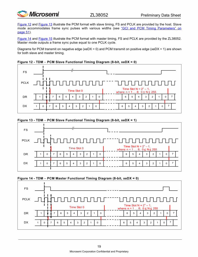
Figure 12 and Figure 13 illustrate the PCM format with slave timing, FS and PCLK are provided by the host. Slavemode accommodates frame sync pulses with various widths (see “GCI and PCM Timing Parameters” onpage 51).
Figure 14 and Figure 15 illustrate the PCM format with master timing, FS and PCLK are provided by the ZL38052.Master mode outputs a frame sync pulse equal to one PCLK cycle.
Diagrams for PCM transmit on negative edge (xeDX = 0) and PCM transmit on positive edge (xeDX = 1) are shownfor both slave and master timing.
Figure 12 - TDM PCM Slave Functional Timing Diagram (8-bit, xeDX = 0)
Figure 13 - TDM PCM Slave Functional Timing Diagram (8-bit, xeDX = 1)
Figure 14 - TDM PCM Master Functional Timing Diagram (8-bit, xeDX = 0)
567 4 123 01 0 123 056 4 7
567 4 123 01 0 123 056 4 7
FS
PCLK
DR
DX
Time Slot 0Time Slot N = 2n – 1,
where: n = 1 … 8; 0 N 255
567 4 123 01 0 123 056 4 7
567 4 123 01 0 123 056 4 7
FS
PCLK
DR
DX
Time Slot 0Time Slot N = 2n – 1,
where: n = 1 … 8; 0 N 255
567 4 123 01 0 123 056 4 7
567 4 123 01 0 123 056 4 7
FS
PCLK
DR
DX
Time Slot 0Time Slot N = 2n – 1,
where: n = 1 … 8; 0 N 255
19
Microsemi Corporation Confidential and Proprietary

ZL38052 Preliminary Data Sheet
Figure 15 - TDM PCM Master Functional Timing Diagram (8-bit, xeDX = 1)
4.1.3 GCI Mode
The GCI voice/data bytes can occupy any of the available timeslots. The GCI block can be configured as a masteror a slave and supports a clock that has the same frequency as the data rate.
Note: Traditional GCI Monitor, Signalling, and Control channel bytes and double data rate are not supported.
Figure 16 illustrates the GCI format with slave timing, FS and PCLK are provided by the host. Slave modeaccommodates frame sync pulses with various widths (see “GCI and PCM Timing Parameters” on page 51).
Figure 17 illustrates the GCI format with master timing, FS and PCLK are provided by the ZL38052. Master modeoutputs a frame sync pulse equal to one PCLK cycle.
For both, first data bits are aligned with the rising edge of the frame sync pulse.
Figure 16 - TDM GCI Slave Functional Timing Diagram
567 4 123 01 0 123 056 4 7
567 4 123 01 0 123 056 4 7
FS
PCLK
DR
DX
Time Slot 0Time Slot N = 2n – 1,
where: n = 1 … 8; 0 N 255
456 3 012 70 7 012 745 3 6
456 3 012 70 7 012 745 3 6
Time Slot 0Time Slot N = 2n – 1,
where: n = 1 … 8; 0 N 255
FS
PCLK
DR
DX
20
Microsemi Corporation Confidential and Proprietary

ZL38052 Preliminary Data Sheet
Figure 17 - TDM GCI Master Functional Timing Diagram
4.2 Cross Point Switch
The ZL38052 contains a Cross Point Switch that allows any input port to be routed to any output port as well asrouting the input/outputs to/from the audio processor functions. Refer to the Microsemi AcuEdge™ TechnologyZLS38052 Firmware Manual for Cross Point Switch operation and control.
4.3 Host Bus Interface
The host bus interface (HBI) is the main communication port from a host processor to the ZL38052. It can beconfigured to be either a SPI Slave or an I2C Slave port, either of which can be used to program or query thedevice.
The ZL38052 allows for automatic configuration between SPI and I2C operation. For the HBI port, if the HCLKtoggles for two cycles, the HBI will default to the SPI Slave, otherwise it will remain configured as I2C (see Table 2).The HBI comes up listening in both SPI and I2C modes, but with I2C inputs selected. If HCLK is present, it switchesthe data selection before the first byte is complete so that no bits are lost. Once the port is determined to be SPI, ahardware reset is needed to change back to I2C.
This port can read and write all of the memory and registers on the ZL38052. The port can also be used to boot thedevice, refer to “Device Booting and Firmware Swapping” on page 31.
Table 2 - HBI Slave Interface Selection
Note 1: By default, the HBI comes up as an I2C interface. Toggling the HCLK pin will cause the host interface to switch to a SPI interface. If an I2C interface is desired, HCLK needs to be tied to ground.
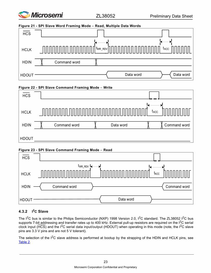
4.3.1 SPI Slave
The physical layer is a 4-wire SPI interface. Chip select and clock are both inputs.
The SPI Slave port can support byte, word, or command framing. Write and read diagrams for these framing modesare shown in Figure 18 Figure 23. The SPI Slave chip select polarity, clock polarity, and sampling phase are fixed.
Description Condition Operating Mode Notes
HBI Slave interface selection. HCLK toggling Host SPI bus
HDIN tied to VSS Host I2C bus. Slave address 45h (7-bit).1
HDIN tied to DVDD33 Host I2C bus. Slave address 52h (7-bit).
FS
PCLK
DR
DX
456 3 012 70 7 012 745 3 6
456 3 012 70 7 012 745 3 6
Time Slot 0Time Slot N = 2n – 1,
where: n = 1 … 8; 0 N 255
21
Microsemi Corporation Confidential and Proprietary

ZL38052 Preliminary Data Sheet
The ZL38052 command protocol is half duplex, allowing the serial in and serial out to be shorted together for a 3-wire connection. The chip select is active low. The data is output on the falling edge of the clock and sampled on therising edge of the clock.
The SPI Slave supports access rates up to 25 MHz.
The outbound interrupt is always active low.
Figure 18 - SPI Slave Byte Framing Mode Write
Figure 19 - SPI Slave Byte Framing Mode Read
Figure 20 - SPI Slave Word Framing Mode Write, Multiple Data Words
HCS
HCLK
HDIN
HDOUT
Cmd_wd[15:8] Cmd_wd[7:0] Data_wd[15:8] Data_wd[7:0]
tACC tACCtACC
tACC
Cmd_wd
HCS
HCLK
HDIN
HDOUT
Cmd_wd[15:8] Cmd_wd[7:0]
Data_wd[15:8] Data_wd[7:0]
tACC tWR_RDVtACC
tACC
Cmd_wd
HCS
HCLK
HDIN
HDOUT
Command word Data word
tACC tACC
Data word
22
Microsemi Corporation Confidential and Proprietary
ZL38052 Preliminary Data Sheet
Figure 21 - SPI Slave Word Framing Mode Read, Multiple Data Words
Figure 22 - SPI Slave Command Framing Mode Write
Figure 23 - SPI Slave Command Framing Mode Read
4.3.2 I2C Slave
The I2C bus is similar to the Philips Semiconductor (NXP) 1998 Version 2.0, I2C standard. The ZL38052 I2C bussupports 7-bit addressing and transfer rates up to 400 kHz. External pull-up resistors are required on the I2C serialclock input (HCS) and the I2C serial data input/output (HDOUT) when operating in this mode (note, the I2C slavepins are 3.3 V pins and are not 5 V tolerant).
The selection of the I2C slave address is performed at bootup by the strapping of the HDIN and HCLK pins, seeTable 2.
HCS
HCLK
HDIN
HDOUT
Command word
Data word
tWR_RDV tACC
Data word
HCS
HCLK
HDIN
HDOUT
Command word Data word
tACC
Command word
HCS
HCLK
HDIN
HDOUT
Command word
Data word
tACC
Command word
tWR_RDV
23
Microsemi Corporation Confidential and Proprietary

ZL38052 Preliminary Data Sheet
4.3.3 UART
The ZL38052 device incorporates a two-wire UART (Universal Asynchronous Receiver Transmitter) interface with afixed 115.2K baud transfer rate, 8 data bits, 1 stop and no parity. TX and RX pins allow bi-directional communicationwith a host. The UART pins must be made accessible on the PCB for debug and tuning purposes.
The UART port can be used as a debug tool and is used for tuning purposes.
4.3.4 Host Interrupt Pin
An internal host interrupt controller controls the active low interrupt pin which is part of the host bus interface.Associated with the interrupt controller is an event queue which reports status information for the interrupt.
Upon sensing the interrupt, the host reads the event queue to determine which event caused the interrupt. Eventsare enabled by the host processor, and are typically not used in a standalone (controllerless) design.
Refer to Events in the Microsemi AcuEdge™ Technology ZLS38052 Firmware Manual for Event ID Enumerations.
4.4 Master SPI
Like the HBI SPI Slave, the physical layer of the Master SPI is a 4-wire SPI interface supporting half duplexcommunication. It supports only one chip select which is multiplexed with GPIO_9.
The Master SPI is only accessible through boot ROM commands and is only used as the boot loading mechanismfrom an external serial Flash. The ZL38052 can automatically read the Flash data (program code and configurationrecord) through this interface upon the release of reset (Auto Boot), depending on the value of the bootstrapoptions.
Note: An alternative to Auto Boot is to perform a Host Boot through the HBI port. Refer to 7.0, “Device Booting andFirmware Swapping“ on page 31.
4.4.1 Flash Interface
After power-up the ZL38052 will run its resident boot code, which establishes the initial setup of the Master SPI portand then loads the firmware from external Flash memory. This Flash firmware establishes the resident applicationand sets the modes of all the ZL38052 ports.
Figure 24 illustrates the connection of Flash memory to the ZL38052 Master SPI port. A 2 Mbit Flash is theminimum size required to store the program code and the configuration record of the ZL38052 device. TheZLE38000 demonstration hardware uses the MacronixTM MX25L4006E 4 Mbit CMOS Serial Flash device.
24
Microsemi Corporation Confidential and Proprietary

ZL38052 Preliminary Data Sheet
Figure 24 - Flash Interface Circuit
4.4.1.1 Flash Selection
The ZL38052 Boot ROM is designed to work with a wide variety of Flash devices. There are numerous Flashdevices that the ZL38052 Boot ROM can recognize and program without host intervention other than a command toinitialize the Flash. Other unrecognized devices may be utilized if they conform to characteristics of known devicesand the host informs the ZL38052 Boot ROM of their type and size.
The ZL38052 identifies Flash devices (with a single binary image) with the ZL38052 boot ROM auto sensing theFlash type that complies with JEDEC Manufacturer and Device ID Read Methodology for SPI Compatible SerialInterface Memory Devices. The ZL38052 utilizes the Serial Flash Discoverable Parameters JEDEC standardJESD216B and the Common Flash Interface JESD68.01 JEDEC standard. The ZL38052 can identify devices bytheir JEDEC standard JEP106-K Standard Manufacturer’s Identification Code.
A list of Flash devices that are identifiable by the ZL38052 Boot ROM are shown in Table 3. The size of thesedevices are all 2 Mbit or 4 Mbit, the Boot ROM will also recognize the size of 8 Mbit parts that are Type 1 or Type 2devices (as defined in Table 4).
ZL38052
SM_CS
+3.3 V
SM_CLK
100 nF
SM_MISO
SM_MOSI
SCLK
CS
SO/SIO1
SI/SIO0
HOLD
WP
VCC
GND
10K10K100K 100K
Master SPI
MX25L4006E
25
Microsemi Corporation Confidential and Proprietary

ZL38052 Preliminary Data Sheet
Table 3 - Flash Devices Tested with the ZL38052
Flash devices whose JEDEC ID or size (usually a size of 16 Mbit or larger) that are not recognized by the ZL38052Boot ROM can be made to work if they fit the characteristics of one of the 4 Flash types listed in Table 4. By writingthe type (1, 2, 3, or 4) to ZL38052 address 0x118 and the number of sectors to ZL38052 address 0x116 prior toinitializing the Flash device, the Boot ROM will treat it as a known device of known size even though themanufacturer ID or size field are not recognized. Once the Flash is initialized, which erases and writes the Flashheader, the Flash will work as a recognized Flash for all reading and programming operations.
Manufacturer Part Number Description
Macronix™ MX25V4006EM1I-13G 4 Mbit Flash.
Winbond™ W25X40CLSNIG-ND 4 Mbit Flash.
W25X20CLSNIG-ND 2 Mbit Flash.
Micron® M25P20-VMN6PB 2 Mbit Flash. Large 512 Kbit sectors limit theusefulness of this device. Holds only 1 applicationimage.
M25P40-VMN6PB 4 Mbit Flash. Large 512 Kbit sectors limit theusefulness of this device. Holds only 2 or 3application images.
Microchip™ SST25VF020B-80-4I 2 Mbit Flash.
Atmel® AT25DF041A
AT45DB041D
4 Mbit Flash. Must be used in its 256 byte pagevariant. The default configuration is a 264 bytepage. It can be ordered or programmed to use a256 byte page.
Spansion™ S25FL204K0TMF1010 4 Mbit Flash.
AMIC Technology
A25L020O-F 2 Mbit Flash.
26
Microsemi Corporation Confidential and Proprietary

ZL38052 Preliminary Data Sheet
Table 4 - Supported Flash Types
4.5 GPIO
The ZL38052 64-pin QFN package has 14 GPIO (General Purpose Input/Output) pins; the ZL38052 56-ballWLCSP package has 11 GPIO pins.
The GPIO can be individually configured as either inputs or outputs, and have associated maskable interruptsreported to the host processor through the interrupt controller and event queue. The GPIO pins are intended for lowfrequency signalling.
When a GPIO pin is defined as an input, the state of that pin is sampled and latched into the GPIO Read Register.A transition on a GPIO input can cause an interrupt and event to be passed to the host processor.
Certain GPIO pins have special predefined functions, such as volume up/down, associated with that pin. IndividualGPIO pins may also be defined as status outputs. See Fixed Function I/O in the Microsemi AcuEdge™ TechnologyZLS38052 Firmware Manual.
Characteristic Type 1 Type 2 Type 3 Type 4
Sector Size 512 Kbit (64 KB) 32 Kbit (4 KB) 32 Kbit (4 KB) 16 Kbit (2 KB)
Read Status Reg Cmd 0x05 0x05 0x05 0xD7
Status Reg Busy bit = 0x01 Busy bit = 0x01 Busy bit = 0x01 Done bit = 0x80
Data Read Cmd 0x03 0x03 0x03 0x03
Write Enable Cmd 0x06 0x06 0x06 N/A
Page Write Cmd 0x02 0x02 N/A
Uses AAI toprogram word orbyte. Uses WriteDisable commandto terminate AAI.
N/A
Uses write frombuffer command.
4-Byte Bulk Erase Cmd N/A N/A N/A 0xC794809A
Examples Micron®
M25P20-VMN6PB
M25P40-VMN6PB
Winbond™
W25X40CLSNIG-ND
W25X20CLSNIG-ND
Macronix™
MX25V4006EM1I-13G
AMIC Technology
A25L020O-F
Spansion™
S25FL204K0TMF1010
Atmel®
AT25DF041A
Microchip™
SST25VF020B-80-4I
Atmel®
AT45DB021D
AT45DB041D
27
Microsemi Corporation Confidential and Proprietary
ZL38052 Preliminary Data Sheet
In addition to the predefined fixed functions and the general functionality of the GPIO pins, certain GPIO pins alsosupport bootstrap functions. Immediately after any power-on or hardware reset the GPIO pins are defined as inputsand their state is captured in the GPIO Configuration Register. The state of this register is used to determine whichoptions are selected for the device. The GPIO pin status is then redefined as specified in the configuration recordupon a load from the Flash or host. A list of bootstrap modes are found in Table 6.
5.0 Reset
The device has a hardware reset pin (RESET) that places the entire device into a known low power state. Thedevice will perform either a digital or an analog reset depending on the duration of the reset pulse.
• Digital reset When the reset pin is brought low for a duration of between 100 ns and 1 s, a digital reset occurs and all device states and registers are reset by this pin.
• Analog reset When the reset pin is brought low for a duration greater than 10 s, both a digital and an analog reset will occur. The analog reset will deactivate the internally generated +1.2 V by shutting off the external FET and the internal PLL. Raising the reset pin high will immediately turn back on these supplies (requiring a corresponding PLL startup time, ~3 ms).
For both digital and analog reset cases when reset is released, the device will go though its boot process and thefirmware will be reloaded. If the reset had been an analog reset, then the boot process will take longer waiting forthe system clocks to power back on.
GPIO sensing will occur with either type of reset.
A 10 K pull-up resistor is required on the RESET pin to DVDD33 if this pin is not continuously driven.
6.0 Power Supply
6.1 Power Supply Sequencing/Power up
No special power supply sequencing is required. The +3.3 V or +1.2 V power rails can be applied in either order.
Upon power-up, the ZL38052 begins to boot and senses the external resistors on the GPIO pins to determine thebootstrap settings. After 3 ms, the boot process begins and the ZL38052 takes less than 1 second to become fullyoperational (when auto-booting from Flash, including the time it takes to load the firmware).
In order to properly boot, the clocks to the device must be stable. This requires either the 12.000 MHz crystal oroscillator to be active, or the PCLK and frame sync of TDM-A be present and stable before the ZL38052’s reset isreleased.
6.1.1 Power Supply Considerations
The ZL38052 requires +1.2 V to power its core DSP power supply (DVDD12). To achieve optimum noise and powerperformance, supply DVDD12 from an external source. Use an LDO regulator like the Microsemi LX8213 toachieve low noise and low overall power consumption. The ZL38052 is designed to minimize power in its activestates when DVDD12 is supplied externally.
To further reduce power when using a crystal or clock oscillator, the internal PLL can be shut-down as described in6.1.1.3, “Ultra-Low Power Mode“.
6.1.1.1 External +1.2 V Power
Figure 25 shows DVDD12 powered from an external supply. A Microsemi LX8213 300 mA Low Noise CMOS LDORegulator is shown.
External supply is specified when the EXT_SEL pin is tied to +3.3 V. The EXT_SEL pin can be pulled high or simplyhard-wired to DVDD33.
28
Microsemi Corporation Confidential and Proprietary

ZL38052 Preliminary Data Sheet
VDD12_CTRL is a CMOS output which can be used to control the shutdown of the external supply. VDD12_CTRLwill provide a steady +3.3 V output (with up to 4 mA of source current) for the external supply to be enabled and 0 Vfor the supply to be disabled.
For power savings when the ZL38052 does not need to be operational, the external voltage regulator can beturned off by pulling the RESET pin low for longer than 10 S (Reset mode). This action will force theVDD12_CTRL pin low, shutting off the external LDO and allowing the +1.2 V supply to collapse to 0 V.
If shutdown of the external +1.2 V supply is not desired, simply leave the VDD12_CTRL output pin floating.
Figure 25 - External +1.2 V Power Supply Configuration
6.1.1.2 Internal +1.2 V Power
Note: The internal +1.2 V power option is only available with the 64-pin QFN package. The VDD12_CTRL pin is not avail-able on the 56-ball WLCSP package.
Alternatively, the ZL38052 has a built-in voltage regulator that can be used as the DVDD12 source. The internalvoltage regulator requires an external N-channel FET device and a parallel 470 ohm resistor. Figure 26 showsDVDD12 powered from the internal supply. Power dissipation is higher with internal regulator use due to theinternal control circuitry and functional blocks being active.
Internal supply use is selected when the EXT_SEL pin is tied to VSS. With the built-in voltage regulator enabled,VDD12_CTRL will drive Q1 and generate +1.2 V at DVDD12. The parallel 470 ohm resistor is required to ensuresupply start-up. Q1 can be any of the high power FETs shown in Table 5, or an equivalent.
For power savings when the ZL38052 does not need to be operational, the internal voltage regulator can beturned off by pulling the RESET pin low for longer than 10 S (Reset mode). This action will force theVDD12_CTRL pin low, shutting off the FET and allowing the +1.2 V supply to collapse to 0 V.
VSS
VDD12_CTRL
DVDD12
DVDD33 +3.3 V
ZL38052
LDO
SHDN
+1.2 V
GND
EXT_SEL
+3.3 VVINVOUT
Supply decoupling is not shown
RESET
LX8213
29
Microsemi Corporation Confidential and Proprietary

ZL38052 Preliminary Data Sheet
Figure 26 - Internal +1.2 V Power Supply Configuration
Table 5 - Q1 Component Options
6.1.1.3 Ultra-Low Power Mode
Note: Ultra-low power mode is only available with the 64-pin QFN package. The DVDD33_XTAL pin is not available on the 56-ball WLCSP package.
When using a crystal or clock oscillator, the ZL38052 can be placed into an Ultra-low power state by turning off thecrystal oscillator’s internal voltage regulator. The circuit required to perform this is shown in Figure 27.
The external circuit that drives the ZL38052 RESET pin can also be used to power the DVDD33_XTAL pin. Thereset drive circuit (gate) needs to provide at least 10 mA of source current when reset is high. The series 100 ohmresistor provides a time delay to keep crystal power from reacting to short reset pulses. When the reset line goeslow for longer than 10 S, the crystal oscillator’s internal regulator will turn off and the ZL38052 will draw Ultra-lowpower as specified in “Device Operating Modes” on page 43.
Manufacturer Part Number
Vishay® Si1422DH
International Rectifier IRLMS2002
Diodes Inc.® ZXMN2B03E6
VSS
VDD12_CTRL
DVDD12
DVDD33 +3.3 V
ZL38052
EXT_SEL
470
Q1
G
D
S
G
Supply decoupling is not shown
RESET
30
Microsemi Corporation Confidential and Proprietary

ZL38052 Preliminary Data Sheet
Figure 27 - Ultra-Low Power Operation Circuit
7.0 Device Booting and Firmware Swapping
7.1 Boot Loader
The ZL38052 device contains a built-in boot-loader that gets executed after a hardware reset, when power isinitially applied to the part, and during the Firmware Swap process. The Bootloader performs the following actions:
• Reads the GPIO bootstrap information and stores it in the Boot Sense registers
• Depending on the bootstrap setting, it loads the external serial Flash device contents (firmware and configuration record) into Program RAM (Auto Boot), or waits for the host to load Program RAM (Host Boot and Firmware Swap)
• If Auto Boot is selected, the Bootloader then programs the ZL38052 configuration registers to their proper default values, and jumps to Program RAM to execute the firmware
7.2 Bootstrap Modes
Table 6 lists the different boot options that can be selected by using external resistors. These GPIOs have internalpull-down resistors, thereby defaulting to a 0 setting. A resistor to DVDD33 is required to select a 1 option. Theexternal pull-up resistors must have a value of 3.3 K. A GPIO with a bootstrap pull-up can be used for otherfunctionality following the power-up boot sense process.
Table 6 - Bootstrap Modes
X = Don’t care.
Note 1: Apply a 3.3 K resistor from GPIO_0 to DVDD33.
Note 2: Apply a 3.3 K resistor from GPIO_1 to DVDD33.
Note 3: Apply a 3.3 K resistor from GPIO_2 to DVDD33. Note, when external Flash is selected, GPIO_9 = SM_CS.
GPIO_2 GPIO_1 GPIO_0 Operating Mode Description Notes
X 0 0 Crystal source 12 MHz (default) Clock source selection
X 0 1 TDM FSA source is 8 kHz 1
X 1 0 TDM FSA source is 16 kHz 2
X 1 1 Reserved
0 X X Host Boot (default) Boot source selection
1 X X Auto Boot from external Flash 3
ZL38052
DVDD33_XTAL
Reset
100Crystalor OSC
XI
XO
0.1uF
RESET
31
Microsemi Corporation Confidential and Proprietary

ZL38052 Preliminary Data Sheet
7.3 Loadable Device Code
In order for the ZL38052 to operate, it must be loaded with code that resides externally. This code can either bebooted from an external Flash memory through the Master SPI, or can be loaded into the ZL38052 by the hostprocessor through the HBI port. During power-on and hardware reset, an external resistor pull-up or an internalresistor pull-down determines which boot mode will be used (see Table 6). During a Firmware Swap, the hostselects which mode will be used.
The external code consists of two logical segments, the firmware code itself and the configuration record. Thefirmware is a binary image which contains all of the executable code allowing the ZL38052 to perform voiceprocessing or sound detection and establishes the user command set. The configuration record contains settingsfor all of the user registers and defines the power-up operation of the device.
For an application that has no host and no way of externally programming the ZL38052, the configuration record issetup so that the registers are set to their desired values for normal operation. In this situation there is no way toperform a Firmware Swap. The ZL38052 will remain in either voice processing or sound detection mode.
A GUI development tool (MiTuner™ ZLS38508) is provided to create and modify the configuration record andcreate a bootable Flash image which can then be duplicated for production of the end product. This tool requiresaccess to the UART and to the I2S port for tuning (refer to 12.0, “AEC Tuning“ on page 59).
7.3.1 Booting and Firmware Swapping Speed
When performing an Auto Boot or Firmware Swap from a Flash device the boot sequence lasts <1 second.
When performing a Host Boot or Firmware Swap through the HBI SPI/I2C Slave port, the boot time will varydepending on the host's communications speed. The SPI port can run up to a speed of 25 MHz and has lessoverhead, allowing it to perform a boot download ~<300 ms; I2C is limited to a speed of 400 kHz, making a bootdownload last ~>5 seconds. If boot speed is important, the HBI SPI Slave port should be used for booting ratherthan the I2C Slave port.
7.4 Bootup Procedure
Valid clocks (PCLKA/FSA or a crystal or oscillator) must be present before the ZL38052 device can exit its resetstate. After the reset line is released, the ZL38052’s internal voltage regulator will be enabled (if the EXT_SEL pin isstrapped low). Once the +1.2 V supply is established, the PLL will be also be enabled. Based on the GPIObootstrap options, the ZL38052 will select the appropriate PLL source and system parameters and the PLL will lockto the desired operating frequency. An event will be placed in the event-queue and the interrupt pin (HINT) will bepulled low to signal the host when it’s OK to load boot code.
Next, if the GPIO strapping pins indicate that the ZL38052 will Auto Boot, it will begin reading data from the externalFlash. Refer to the Microsemi AcuEdge™ Technology ZLS38052 Firmware Manual for a listing of the completeBoot Sequence.
If the GPIO strapping pins indicate that the ZL38052 will Host Boot, the SPI or I2C port that initiates the loadingprocess becomes the boot master. The ZL38052 allows for automatic configuration between SPI and I2C operation.For the HBI port, if the HCLK toggles for two cycles, the HBI will default to the SPI Slave, otherwise it will remainconfigured as I2C.
32
Microsemi Corporation Confidential and Proprietary

ZL38052 Preliminary Data Sheet
8.0 Device Pinouts
8.1 64-Pin QFN
Figure 28 - ZL38052 64-Pin QFN Top View
64 585960616263 57 56 55 54
11
10
9
8
7
6
5
4
3
2
1
DR
B/I2
S_S
DIB
GP
IO_9
/SM
_CS
PC
LKB
/I2S
_SC
KB
FSB
/I2S
_WS
B
DV
DD
12
DV
DD
33
HD
OU
T
UA
RT
_TX
VS
S
DX
B/I2
S_S
DO
B
53 52 51 50 49
16
15
14
13
12
38
39
40
41
42
43
44
45
46
47
48
33
34
35
36
37
32313029282726252423222120191817
HC
LK
DV
DD
33
UA
RT
_RX
HC
S
HIN
TDVDD33
GPIO_10
GPIO_8
DVDD12
GPIO_7
GPIO_6
GPIO_12
GPIO_2
GPIO_5
GPIO_4
GPIO_0
GPIO_3
DVDD33
GPIO_13
GPIO_1
FSA
/I2S
_WS
A
DR
A/I2
S_S
DIA
DM
IC_I
N1
NC
DV
DD
33 NC
XO
DV
DD
12
DM
IC_C
LK NC
EX
T_S
EL
DM
IC_I
N2
DX
A/I2
S_S
DO
A
SM_CLK
SM_MISO
SM_MOSI
DVDD33
DAC1_M
DAC1_P
DAC2_P
CDAC
CREF
RESET
DVDD12
GPIO_11
AVDD33
DAC2_M
DVDD12
AVDD33
HD
IN
Exposed Ground Pad
VDD12_CTRL
XI
DV
DD
33_X
TA
L
PC
LKA
/I2S
_SC
KA
33
Microsemi Corporation Confidential and Proprietary

ZL38052 Preliminary Data Sheet
8.2 56-Ball WLCSP
Figure 29 - ZL38052 56-Ball WLCSP Top View
NC XIDMIC_CLKNCDMIC_IN1DMIC_IN2DXA/I2S_SDOA
H1 H2 H3 H4 H5 H6 H7
CREFDVDD12DVDD12NCDVDD33DRA/I2S_SDIA VSS
G1 G2 G3 G4 G5 G6 G7
XO CDACGPIO_2 GPIO_0GPIO_3FSA/I2S_WSA GPIO_5
F1 F2 F3 F4 F5 F6 F7
GPIO_10GPIO_7 AVDD33VSSGPIO_1PCLKA/I2S_SCKA GPIO_6
E1 E2 E3 E4 E5 E6 E7
GPIO_8 RESET DAC2_PVSSVSSDVDD12
D1 D2 D3 D4 D5 D6 D7
GPIO_11 DAC1_PPCLKB/I2S_SCKBHINT UART_TX
C1 C2 C3 C4 C5 C6 C7
DVDD33VSSDVDD12VSSDVDD33HCS UART_RX
B1 B2 B3 B4 B5 B6 B7
SM_MOSISM_MISOSM_CLKGPIO_9/SM_CSHDOUTHDINHCLK
A1 A2 A3 A4 A5 A6 A7
DRB/I2S_SDIB DXB/I2S_SDOB
FSB/I2S_WSB
34
Microsemi Corporation Confidential and Proprietary

ZL38052 Preliminary Data Sheet
9.0 Pin Descriptions
Table 7 - Reset Pin Description
Table 8 - DAC Pin Descriptions
Table 9 - Microphone Pin Descriptions
Table 10 - TDM and I2S Ports Pin Descriptions
The ZL38052 device has two TDM interfaces, TDM-A and TDM-B. Each TDM block is capable of being a master or
QFNPin #
WLCSP Ball Name Type Description
15 D6 RESET Input Reset. When low the device is in its reset state and all tristate outputs will be in a high impedance state. This input must be high for normal device operation. A 10 K pull-up resistor is required on this node to DVDD33 if this pin is not continuously driven.
Refer to “Reset” on page 28 for an explanation of the various reset states and their timing.
QFNPin #
WLCSP Ball Name Type Description
6 DAC1_M Output DAC 1 Minus Output. This is the negative output signal of the differential amplifier of the DAC 1. Not available on the WLCSP package.
7 C7 DAC1_P Output DAC 1 Plus Output. This is the positive output signal of the differential amplifier of the DAC 1.
9 DAC2_M Output DAC 2 Minus Output. This is the negative output signal of the differential amplifier of the DAC 2. Not available on the WLCSP package.
8 D7 DAC2_P Output DAC 2 Plus Output. This is the positive output signal of the differential amplifier of the DAC 2.
12 F7 CDAC Output DAC Reference. This pin requires capacitive decoupling. Refer to “DAC Bias Circuit” on page 13.
13 G7 CREF Output Common Mode Reference. This pin requires capacitive decoupling. Refer to “DAC Bias Circuit” on page 13.
QFNPin #
WLCSP Ball Name Type Description
18 H6 DMIC_CLK Output Digital Microphone Clock Output. Clock output for digital microphones and digital electret microphone pre-amplifier devices.
19 H3 DMIC_IN1 Input Digital Microphone Input 1. Stereo or mono digital microphone input. Tie to VSS if unused.
20 H2 DMIC_IN2 Input Digital Microphone Input 2. Stereo or mono digital microphone input.Tie to VSS if unused.
35
Microsemi Corporation Confidential and Proprietary

ZL38052 Preliminary Data Sheet
a slave. The ports can be configured for Pulse-Code Modulation (PCM) or Inter-IC Sound (I2S) operation. Theports conform to PCM, GCI, and I2S timing protocols.
QFNPin #
WLCSP Ball Name Type Description
29 E1 PCLKA/I2S_SCKA
Input/Output
PCM Port A Clock (Input/Tristate Output). PCLKA is equal to the bit rate of signals DRA/DXA. In TDM master mode this clock is an output and in TDM slave mode this clock is an input.
I2S Port A Serial Clock (Input/Tristate Output). This is the I2S port A bit clock. In I2S master mode this clock is an output and drives the bit clock input of the external slave device’s peripheral converters. In I2S slave mode this clock is an input and is driven from a converter operating in master mode.
After power-up, this signal defaults to be an input in I2S slave mode.
A 100 K pull-down resistor is required on this pin to VSS. If this pin is unused, tie the pin to VSS.When driving PCLKA/I2S_SCKA from a host, one of the following conditions must be satisfied: 1. Host drives PCLKA low during reset, or
2. Host tri-states PCLKA during reset (the 100 K resistor will keep PCLKA low), or
3. Host drives PCLKA at its normal frequency
30 F1 FSA/I2S_WSA
Input/Output
CM Port A Frame Sync (Input/Tristate Output). This is the TDM frame alignment reference. This signal is an input for applications where the PCM bus is frame aligned to an external frame signal (slave mode). In master mode this signal is a frame pulse output.
I2S Port A Word Select (Left/Right) (Input/Tristate Output). This is the I2S port A left or right word select. In I2S master mode word select is an output which drives the left/right input of the external slave device’s peripheral converters. In I2S slave mode this pin is an input which is driven from a converter operating in master mode.
After power-up, this signal defaults to be an input in I2S slave mode.Tie this pin to VSS if unused.
31 G1 DRA/I2S_SDIA
Input PCM Port A Serial Data Stream Input. This serial data stream operates at PCLK data rates.
I2S Port A Serial Data Input. This is the I2S port serial data input.
Tie this pin to VSS if unused.
32 H1 DXA/I2S_SDOA
Output PCM Port A Serial Data Stream Output. This serial data stream operates at PCLK data rates.
I2S Port A Serial Data Output. This is the I2S port serial data output.
36
Microsemi Corporation Confidential and Proprietary

ZL38052 Preliminary Data Sheet
60 C4 PCLKB/I2S_SCKB
Input/Output
PCM Port B Clock (Input/Tristate Output). PCLKB is equal to the bit rate of signals DRB/DXB. In TDM master mode this clock is an output and in TDM slave mode this clock is an input.
I2S Port B Serial Clock (Input/Tristate Output). This is the I2S port B bit clock. In I2S master mode this clock is an output and drives the bit clock input of the external slave device’s peripheral converters. In I2S slave mode this clock is an input and is driven from a converter operating in master mode.
After power-up, this signal is an input in I2S slave mode.Tie this pin to VSS if unused.
61 D5 FSB/I2S_WSB
Input/Output
PCM Port B Frame Sync (Input/Tristate Output). This is the TDM frame alignment reference. This signal is an input for applications where the PCM bus is frame aligned to an external frame signal (slave mode). In master mode this signal is a frame pulse output.
I2S Port B Word Select (Left/Right) (Input/Tristate Output). This is the I2S port B left or right word select. In I2S master mode word select is an output which drives the left/right input of the external slave device’s peripheral converters. In I2S slave mode this pin is an input which is driven from a converter operating in master mode.
After power-up, this signal defaults to be an input in I2S slave mode.Tie this pin to VSS if unused.
62 C5 DRB/I2S_SDIB
Input PCM Port B Serial Data Stream Input. This serial data stream operates at PCLK data rates.
I2S Port B Serial Data Input. This is the I2S port serial data input.
Tie this pin to VSS if unused.
63 C6 DXB/I2S_SDOB
Output PCM Port B Serial Data Stream Output. This serial data stream operates at PCLK data rates.
I2S Port B Serial Data Output. This is the I2S port serial data output.
QFNPin #
WLCSP Ball Name Type Description
37
Microsemi Corporation Confidential and Proprietary
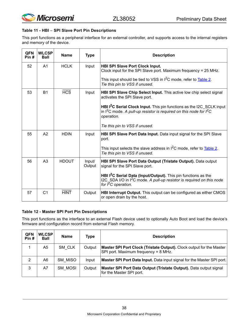
ZL38052 Preliminary Data Sheet
Table 11 - HBI SPI Slave Port Pin Descriptions
This port functions as a peripheral interface for an external controller, and supports access to the internal registersand memory of the device.
Table 12 - Master SPI Port Pin Descriptions
This port functions as the interface to an external Flash device used to optionally Auto Boot and load the device’sfirmware and configuration record from external Flash memory.
QFNPin #
WLCSP Ball Name Type Description
52 A1 HCLK Input HBI SPI Slave Port Clock Input. Clock input for the SPI Slave port. Maximum frequency = 25 MHz.
This input should be tied to VSS in I2C mode, refer to Table 2.Tie this pin to VSS if unused.
53 B1 HCS Input HBI SPI Slave Chip Select Input. This active low chip select signal activates the SPI Slave port.
HBI I2C Serial Clock Input. This pin functions as the I2C_SCLK input in I2C mode. A pull-up resistor is required on this node for I2C operation.
Tie this pin to VSS if unused.
55 A2 HDIN Input HBI SPI Slave Port Data Input. Data input signal for the SPI Slave port.
This input selects the slave address in I2C mode, refer to Table 2.Tie this pin to VSS if unused.
56 A3 HDOUT Input/Output
HBI SPI Slave Port Data Output (Tristate Output). Data output signal for the SPI Slave port.
HBI I2C Serial Data (Input/Output). This pin functions as the I2C_SDA I/O in I2C mode. A pull-up resistor is required on this node for I2C operation.
57 C1 HINT Output HBI Interrupt Output. This output can be configured as either CMOS or open drain by the host.
QFNPin #
WLCSP Ball Name Type Description
1 A5 SM_CLK Output Master SPI Port Clock (Tristate Output). Clock output for the Master SPI port. Maximum frequency = 8 MHz.
2 A6 SM_MISO Input Master SPI Port Data Input. Data input signal for the Master SPI port.
3 A7 SM_MOSI Output Master SPI Port Data Output (Tristate Output). Data output signal for the Master SPI port.
38
Microsemi Corporation Confidential and Proprietary

ZL38052 Preliminary Data Sheet
Table 13 - UART Pin Descriptions
The ZL38052 device incorporates a two-wire UART (Universal Asynchronous Receiver Transmitter) interface with afixed 115.2K baud transfer rate, 8 data bits, 1 stop and no parity. The UART port can be used as a debug tool and isused for tuning purposes.
Table 14 - GPIO Pin Descriptions
GPIO ports can be used for interrupt and event reporting, fixed function control, bootstrap options, as well as beingused for general purpose I/O for communication and controlling external devices.
64 A4 GPIO_9/ SM_CS
Input/Output
Master SPI Port Chip Select (Input Internal Pull-Up/Tristate Output). Chip select output for the Master SPI port.
Shared with GPIO_9, see Table 14.
QFNPin #
WLCSP Ball Name Type Description
50 B2 UART_RX Input UART (Input). Receive serial data in. This port functions as a peripheral interface for an external controller and supports access to the internal registers and memory of the device.
49 C2 UART_TX Output UART (Tristate Output). Transmit serial data out. This port functions as a peripheral interface for an external controller and supports access to the internal registers and memory of the device.
QFNPin #
WLCSP Ball Name Type Description
33, 34,36
F4, E4, F3
GPIO_[0:2] Input/Output
General Purpose I/O (Input Internal Pull-Down/Tristate Output). These pins can be configured as an input or output and are intended for low-frequency signalling. Refer to Table 6 for bootstrap functionality.
37, 38, 39, 40, 41, 43
F2, , F6, E5, E2, D3
GPIO_[3:8] Input/Output
General Purpose I/O (Input Internal Pull-Down/Tristate Output). These pins can be configured as an input or output and are intended for low-frequency signalling. GPIO_4 is not available on the WLCSP package.
64 A4 GPIO_9/ SM_CS
Input/Output
General Purpose I/O (Input Internal Pull-Down/Tristate Output). This pin can be configured as an input or output and is intended for low-frequency signalling.
Alternate functionality with SM_CS, see Table 12.
44, 45,47, 48
E3, C3, ,
GPIO_[10:13]
Input/Output
General Purpose I/O (Input Internal Pull-Down/Tristate Output). These pins can be configured as an input or output and are intended for low-frequency signalling. GPIO_12 and GPIO_13 are not available on the WLCSP package.
QFNPin #
WLCSP Ball Name Type Description
39
Microsemi Corporation Confidential and Proprietary

ZL38052 Preliminary Data Sheet
Table 15 - Oscillator Pin Descriptions
These pins are connected to a 12.000 MHz crystal or clock oscillator which drives the device’s internal PLL.Alternatively, PCLKA can be used as the internal clock source.
QFNPin #
WLCSP Ball Name Type Description
22 H7 XI Input Crystal Oscillator Input. Refer to “External Clock Requirements” on page 48.
23 F5 XO Output Crystal Oscillator Output. Refer to “External Clock Requirements” on page 48.
40
Microsemi Corporation Confidential and Proprietary
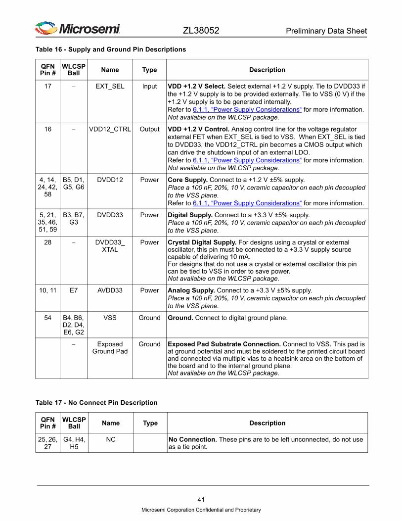
ZL38052 Preliminary Data Sheet
Table 16 - Supply and Ground Pin Descriptions
Table 17 - No Connect Pin Description
QFNPin #
WLCSP Ball Name Type Description
17 EXT_SEL Input VDD +1.2 V Select. Select external +1.2 V supply. Tie to DVDD33 if the +1.2 V supply is to be provided externally. Tie to VSS (0 V) if the +1.2 V supply is to be generated internally. Refer to 6.1.1, “Power Supply Considerations“ for more information. Not available on the WLCSP package.
16 VDD12_CTRL Output VDD +1.2 V Control. Analog control line for the voltage regulator external FET when EXT_SEL is tied to VSS. When EXT_SEL is tied to DVDD33, the VDD12_CTRL pin becomes a CMOS output which can drive the shutdown input of an external LDO.Refer to 6.1.1, “Power Supply Considerations“ for more information.Not available on the WLCSP package.
4, 14, 24, 42,
58
B5, D1, G5, G6
DVDD12 Power Core Supply. Connect to a +1.2 V ±5% supply. Place a 100 nF, 20%, 10 V, ceramic capacitor on each pin decoupled to the VSS plane.Refer to 6.1.1, “Power Supply Considerations“ for more information.
5, 21, 35, 46, 51, 59
B3, B7, G3
DVDD33 Power Digital Supply. Connect to a +3.3 V ±5% supply. Place a 100 nF, 20%, 10 V, ceramic capacitor on each pin decoupled to the VSS plane.
28 DVDD33_XTAL
Power Crystal Digital Supply. For designs using a crystal or external oscillator, this pin must be connected to a +3.3 V supply source capable of delivering 10 mA.For designs that do not use a crystal or external oscillator this pin can be tied to VSS in order to save power.Not available on the WLCSP package.
10, 11 E7 AVDD33 Power Analog Supply. Connect to a +3.3 V ±5% supply. Place a 100 nF, 20%, 10 V, ceramic capacitor on each pin decoupled to the VSS plane.
54 B4, B6, D2, D4, E6, G2
VSS Ground Ground. Connect to digital ground plane.
Exposed Ground Pad
Ground Exposed Pad Substrate Connection. Connect to VSS. This pad is at ground potential and must be soldered to the printed circuit board and connected via multiple vias to a heatsink area on the bottom of the board and to the internal ground plane. Not available on the WLCSP package.
QFNPin #
WLCSP Ball Name Type Description
25, 26, 27
G4, H4, H5
NC No Connection. These pins are to be left unconnected, do not use as a tie point.
41
Microsemi Corporation Confidential and Proprietary

ZL38052 Preliminary Data Sheet
10.0 Electrical Characteristics
10.1 Absolute Maximum Ratings
Stresses above those listed under Absolute Maximum Ratings can cause permanent device failure. Functionality ator above these limits is not implied. Exposure to absolute maximum ratings for extended periods may affect devicereliability.
10.2 Thermal Resistance
Notes:
1. The thermal specifications assume that the device is mounted on an effective thermal conductivity test board (4 layers, 2s2p) per JEDEC JESD51-7 and JESD51-5.
10.3 Operating Ranges
Microsemi guarantees the performance of this device over the industrial (-40 ºC to 85 ºC) temperature range byconducting electrical characterization over each range and by conducting a production test with single insertioncoupled to periodic sampling. These characterization and test procedures comply with the Telcordia GR-357-COREGeneric Requirements for Assuring the Reliability of Components Used in Telecommunications Equipment.
Supply voltage (DVDD33, AVDD33) -0.5 to +4.0 V
Core supply voltage (DVDD12) -0.5 to +1.32 V
Input voltage -0.5 to +4.0 V
Continuous current at digital outputs 15 mA
Reflow temperature, 10 sec., MSL3, per JEDEC J-STD-020 260 C
Storage temperature -55 to +125 C
ESD immunity (Human Body Model) JESD22 Class 1C compliant
Junction to ambient thermal resistance (1), JA 64-pin QFN
56-ball WLCSP
22.1 C/W33.8 C/W
Junction to board thermal resistance (1), JB 64-pin QFN
56-ball WLCSP
6.1 C/W3.9 C/W
Junction to exposed pad thermal resistance (1), JC 64-pin QFN 2.0 C/W
Junction to case thermal resistance (1), JC 56-ball WLCSP 5.2 C/W
Junction to top characterization parameter, JT 64-pin QFN
56-ball WLCSP0.1 °C/W0.3 C/W
Parameter Symbol Min. Typ. Max. Units
Ambient temperature TA -40 +85 C
Analog supply voltage VAVDD333.135 3.3 3.465 VDigital supply voltage VDVDD33
Crystal Digital supply voltage VDVDD33_XTAL
Crystal I/O voltage VXI 2.5 2.625 V
Core supply voltage VDVDD12 1.14 1.2 1.26 V
42
Microsemi Corporation Confidential and Proprietary
ZL38052 Preliminary Data Sheet
10.4 Device Operating Modes
The ZL38052 has six standard modes of operation. Normal operation is when the ZL38052 is running during FullDuplex Communication Mode. Sound Classifier mode is detailed in the ZLS38052 Firmware Guide. Low-Power andSleep modes are programmable options to reduce power consumption. Reset and Ultra-Low Power modes arehardware modes that can be utilized to further minimize power consumption. These are all highlighted in thefollowing sections.
Refer to the Microsemi AcuEdge™ Technology ZLS38052 Firmware Manual for programming and additionalinformation on the firmware operating modes.
10.4.1 Normal (ZLS38052.0)
• Normal firmware mode
• HBI active
• Audio path active
• DACs and MICs can be enabled
• Audio Processor always on
Normal mode is recommended for applications that use the internal voltage regulator with analog microphones.Normal mode keeps the Audio Processor always on, thereby minimizing +1.2 V power supply noise that could beinjected into sensitive analog microphone circuitry via the board layout.
10.4.2 Low-Power (ZLS38052.0)
• Low-Power firmware mode
• HBI active
• Audio path active
• DACs and MICs can be enabled
• Audio Processor operates in Power Saving Mode
Low-power mode is selected in register 0x206 (System Control Flags) bit 1, or can be selected from the ZLS38508MiTuner™ GUI in the AEC Control window (Enable Power Saving Mode). Low-Power mode is not recommendedfor applications that use the internal voltage regulator with analog microphones.
10.4.3 Sound Classifier (ZLS38052.2)
• Glass breaking detection
• Programmable Energy Detector
• Temporal pattern detection
• HBI active
• One MIC active
• DACs disabled
• Audio Processor operates in Power Saving Mode
10.4.4 Sleep (ZLS38052.0)
• Sleep firmware mode
• HBI active
• Audio path inactive
43
Microsemi Corporation Confidential and Proprietary

ZL38052 Preliminary Data Sheet
• DACs and MICs are powered down
• Audio Processor made inactive, internal clocks are shutdown, requires a wake-up procedure to return to Normal or Low-Power mode
The ZL38052 will respond to no other inputs until it awakens from Sleep mode. To wake from Sleep mode, performan HBI Wake From Sleep operation, as described in the ZLS38052 Firmware Manual Appendix D. The firmwareand configuration records loaded into the device RAM are retained, no re-boot is required.
10.4.5 Reset
• Hardware mode, the ZL38052 goes into this mode when the RESET pin is held low for greater than 10 S
• HBI inactive
• Audio path inactive
• DACs and MICs are powered down
• Audio Processor powered down via removal of +1.2 V supply
See 5.0, “Reset“ on page 28 for more information and refer to 6.0, “Power Supply“ on page 28 for information on+1.2 V removal.
10.4.6 Ultra-Low Power
• Hardware mode when using an external crystal or crystal oscillator, the hardware can be configured to enter this mode when the RESET pin is held low for greater than 10 S
• HBI inactive
• Audio path inactive
• DACs and MICs are powered down
• Audio Processor powered down via removal of +1.2 V supply
• Crystal or crystal oscillator supply made inactive
See 5.0, “Reset“ on page 28 and 6.1.1.3, “Ultra-Low Power Mode“ on page 30 for more information, refer to 6.0,“Power Supply“ on page 28 for information on +1.2 V removal.
44
Microsemi Corporation Confidential and Proprietary

ZL38052 Preliminary Data Sheet
10.4.7 Current Consumption
Device current consumption can vary with the firmware load. Common values are listed here using an external+1.2 V supply for the core power supply with PCLKA as the external clock source for the PLL and a 3.3 K resistorfrom GPIO_2 to DVDD33 (external Flash selected), unless otherwise noted.
Note 1: Table values include all current entering DVDD33, AVDD33, and DVDD33_XTAL pins. Add 1.0 mA to Normal, Low-Power, and Sleep modes if the internal voltage regulator is used (EXT_SEL = VSS). Add 1.1 mA to Normal, Low-Power, and Sleep modes if a crystal or crystal oscillator is used (DVDD33_XTAL = +3.3 V).
Note 2: Core supply voltage. Table values include all current entering DVDD12 pins.
Note 3: For 2 DACs active, add 3.6 mA to +3.3 V current.
Note 4: If 3 MICs are active, add 0.6 mA to +1.2 V current.
Note 5: DVDD12 is removed if the internal regulator is used for +1.2 V generation or if the VDD12_CTRL pin is used to shutdown an external +1.2 V LDO that provides DVDD12 to the ZL38052.
+3.3 V 1 +1.2 V 2
Operational Mode Typ. Max. Typ. Max. Units Notes / Conditions
Normal (ZLS38052.0) 9.8 125
mA
Firmware active, power-saving off, 1 DAC active3, 2 MICs active4.
Low-Power (ZLS38052.0)
9.8 87.5 Firmware active, power-saving on,1 DAC active3, 2 MICs active4.
Sleep (ZLS38052.0) 2.5 3.8 Firmware inactive (Firmware and configuration record are retained),DACs and MICs are powered down,HBI is active.
Sound Classifier (ZLS38052.2)
4.5 47.5 Sound Classification Firmware active, 1 MIC active, DACs disabled,HBI is active, **measured in quiet environment
Reset 100 0
A
Device in reset (reset > 10 S), DVDD12 removed5.
Ultra-Low Power 3 0 Crystal or crystal oscillator in use. Device in reset (reset > 10 S), DVDD12 not present, DVDD33_XTAL held low.
45
Microsemi Corporation Confidential and Proprietary
ZL38052 Preliminary Data Sheet
10.5 DC Specifications
Typical values are for TA = 25 ºC and nominal supply voltage. Minimum and maximum values are over the industrial-40 ºC to 85 ºC temperature range and supply voltage range as shown in “Operating Ranges” on page 42, exceptas noted. A 12 MHz crystal oscillator is active.
10.6 AC Specifications
For all AC specifications, typical values are for TA = 25 ºC and nominal supply voltage. Minimum and maximumvalues are over the industrial -40 ºC to 85 ºC temperature range and supply voltage ranges as shown in “OperatingRanges” on page 42, except as noted. A 12.000 MHz crystal oscillator is active, ZL38052 in Normal, Widebandoperational mode.
10.6.1 Microphone Interface
Parameter Symbol Min. Typ. Max. Units Notes / Conditions
Input high voltage VIH 0.7 * VDVDD33
VDVDD33 + 0.3
V All digital inputs
Input low voltage VIL VVSS - 0.3 0.3 * VDVDD33
V All digital inputs
Input hysteresis voltage VHYS 0.4 V
Input leakage (input pins) IIL 5 A 0 to3.3 V
Input leakage (bi-directional pins) IBL 5 A 0 to +3.3 V
Weak pull-up current IPU 38 63 101 A Input at 0 V
Weak pull-down current IPD 19 41 158 A Input at +3.3 V
Input pin capacitance CI 5 pF
Output high voltage VOH 2.4 V At 12 mA
Output low voltage VOL 0.4 V At 12 mA
Output high impedance leakage IOZ 5 A 0 to3.3 V
Pin capacitance (output & input/tristate pins)
CO 5 pF
Output rise time tRT 1.25 ns 10% to 90%, CLOAD = 20 pF
Output fall time tFT 1.25 ns 90% to 10%, CLOAD = 20 pF
Parameter Symbol Min. Typ. Max. Units Notes / Conditions
Microphone clock output (DMIC_CLK), 8 kHz, 16 kHz sample rate 48 kHz sample rate
1.0243.072
MHzMHz
DMIC_CLK, Output high current IOH 20 mA VOH = DVDD33 - 0.4 V
DMIC_CLK, Output low current IOL 30 mA VOL = 0.4 V
DMIC_CLK, Output rise andfall time
tR, tF 5 ns CLOAD = 100 pF
46
Microsemi Corporation Confidential and Proprietary

ZL38052 Preliminary Data Sheet
10.6.2 DAC
Measurements taken using PCM mode. THD+N versus output power for speaker drive applications presented inFigure 30; THD+N versus output voltage for amplifier drive applications presented in Figure 31.
Figure 30 - THD+N Ratio versus Output Power Driving Low Impedance
Parameter Symbol Min. Typ. Max. Units Notes / Conditions
DAC output level: Full scale: Differential Single-ended 0 dBm0 : Differential Single-ended
VDACFS 4.82.42.81.4
VPP
DAC gain = 1, 1 K load.
PCM full scale level (Vppd value) 9 dBm0 DAC gain = 1, 600 load
DAC output power: Single-ended, 32 ohm loadSingle-ended, 16 ohm load
Differential, 32 ohm load
20.637.586.0
244794
mW1,Single-ended loads driven capacitively to ground
Frequency response:Sample rate = 48 kS/s
fR20 20000 Hz
1, 3 dB cutoff includes external AC coupling, without AC coupling the response is low pass.
Dynamic range: Sample rate = 48 kS/s 92 dBFS
20 Hz - 20 kHz
Total harmonic distortion plus noise THD + N -82 dBFS 2, Input = -3 dBFS.
Signal to Noise Ratio SNR 85 dB 2,1004 Hz, C-message weighted
Allowable capacitive load to ground CL 100 pF 1, At each DAC output.
Power supply rejection ratio PSRR 50 70 dB 1, 20 Hz - 100 kHz, 100 mVpp supply noise.
Crosstalk -85 -70 dB 1, Between DAC outputs.
Note 1: Guaranteed by design, not tested in production.
Note 2: Single-ended or differential output.
47
Microsemi Corporation Confidential and Proprietary
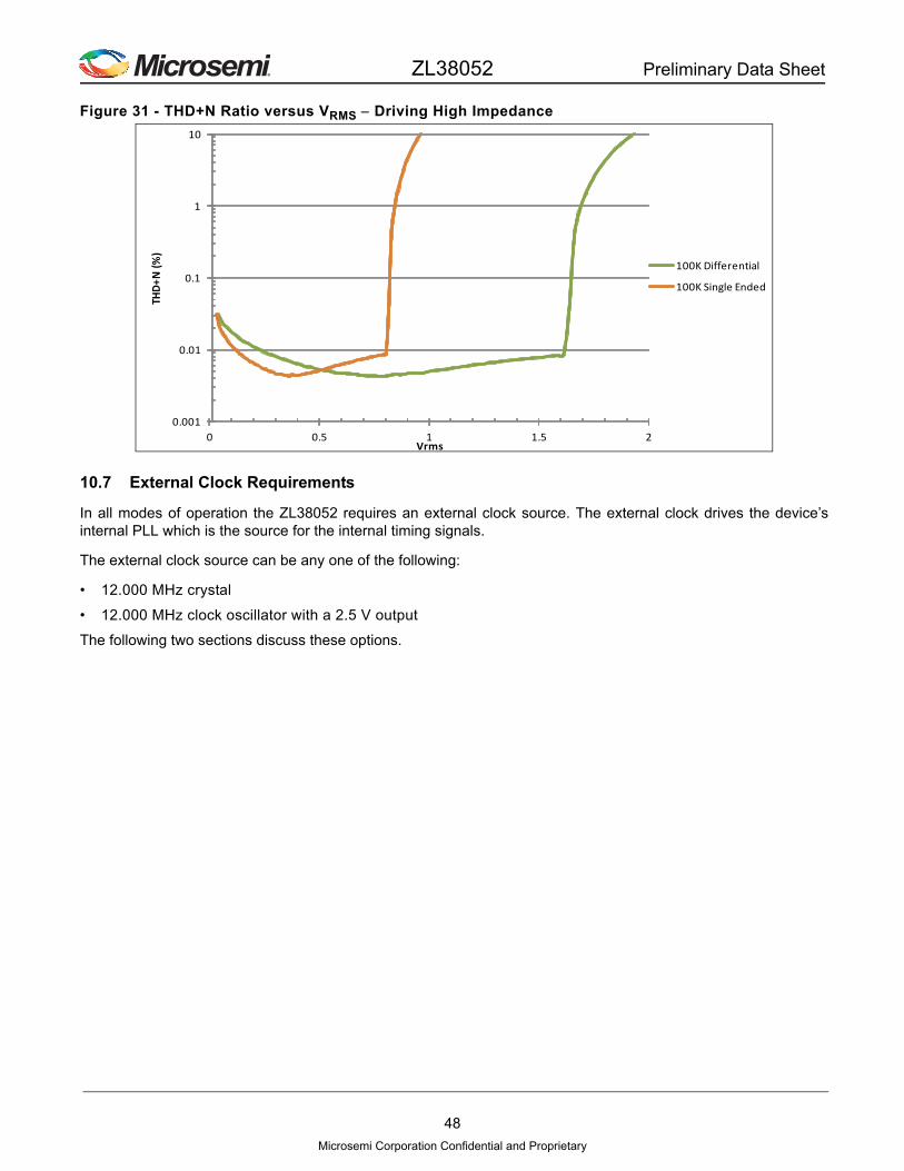
ZL38052 Preliminary Data Sheet
Figure 31 - THD+N Ratio versus VRMS Driving High Impedance
10.7 External Clock Requirements
In all modes of operation the ZL38052 requires an external clock source. The external clock drives the device’sinternal PLL which is the source for the internal timing signals.
The external clock source can be any one of the following:
• 12.000 MHz crystal
• 12.000 MHz clock oscillator with a 2.5 V output
The following two sections discuss these options.
0.001
0.01
0.1
1
10
0 0.5 1 1.5 2
THD+N (%)
Vrms
100K Differential
100K Single Ended
48
Microsemi Corporation Confidential and Proprietary

ZL38052 Preliminary Data Sheet
10.7.1 Crystal Application
The oscillator circuit that is created across pins XI and XO requires an external fundamental mode crystal that hasa specified parallel resonance (fP) at 12.000 MHz.
Figure 32 - Crystal Application Circuit
10.7.2 Clock Oscillator Application
Figure 33 illustrates the circuit that is used when the ZL38052 external clock source is a clock oscillator. Theoscillator pins are 2.5 V compliant and should not be driven from 3.3 V CMOS without a level shifter or voltageattenuator.
Figure 33 - Clock Oscillator Application Circuit
ZL38052
DVDD33_XTAL
+3.3 V
XI
XO
Crystal
DVDD33
PLL
12.000 MHz
20 pF 20 pF
Supply decoupling is not shown
PCLKA/I2S_SCKA100K
PCLKA/I2S_SCKA (if used)
GND (VSS)
ZL38052
DVDD33_XTAL+3.3 V
XI
XO
VDD
DVDD33
PLL
100 nF
12.000 MHz
Oscillator2.5 VOutput
Supply decoupling is not shown
GND (VSS)
PCLKA/I2S_SCKA100K
PCLKA/I2S_SCKA (if used)
49
Microsemi Corporation Confidential and Proprietary

ZL38052 Preliminary Data Sheet
10.7.3 AC Specifications - External Clocking Requirements
These specifications apply to crystal, clock oscillator, or PCLKA external clocking, unless otherwise specified.
11.0 Timing Characteristics
Figure 34 depicts the timing reference points that apply to the timing diagrams shown in this section. For all timingcharacteristics, typical values are for TA = 25 ºC and nominal supply voltage. Minimum and maximum values areover the industrial -40 ºC to 85 ºC temperature range and supply voltage ranges as shown in “Operating Ranges”on page 42, except as noted.
Figure 34 - Timing Parameter Measurement Digital Voltage Levels
Parameter Symbol Min. Typ. Max. Units Notes / Conditions
External clocking frequency accuracy AOSC -50 50 ppm
Not tested in production
External clocking duty cycle DCOSC 40 60 %
PCLKA input jitter 1 nspp
PCLKA or PCLKB output jitter (master mode) 0.75 nspp
PCLKA lock time 200 s
Holdover accuracy 50 ppm Crystal or clock oscillator use only.
Not tested in production.
All DigitalSignals
Timing Reference Points
TiRF/ToRF
VHM
VLMVT
TiRF/ToRF
50
Microsemi Corporation Confidential and Proprietary
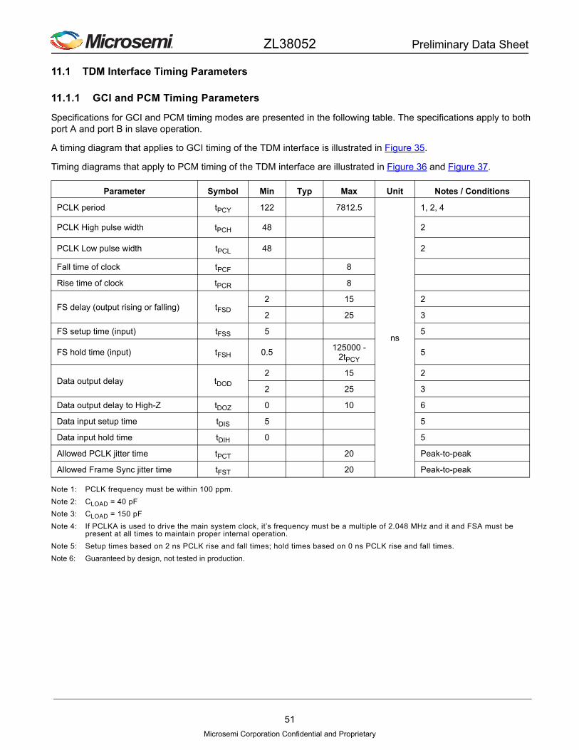
ZL38052 Preliminary Data Sheet
11.1 TDM Interface Timing Parameters
11.1.1 GCI and PCM Timing Parameters
Specifications for GCI and PCM timing modes are presented in the following table. The specifications apply to bothport A and port B in slave operation.
A timing diagram that applies to GCI timing of the TDM interface is illustrated in Figure 35.
Timing diagrams that apply to PCM timing of the TDM interface are illustrated in Figure 36 and Figure 37.
Note 1: PCLK frequency must be within 100 ppm.
Note 2: CLOAD = 40 pF
Note 3: CLOAD = 150 pF
Note 4: If PCLKA is used to drive the main system clock, it’s frequency must be a multiple of 2.048 MHz and it and FSA must be present at all times to maintain proper internal operation.
Note 5: Setup times based on 2 ns PCLK rise and fall times; hold times based on 0 ns PCLK rise and fall times.
Note 6: Guaranteed by design, not tested in production.
Parameter Symbol Min Typ Max Unit Notes / Conditions
PCLK period tPCY 122 7812.5
ns
1, 2, 4
PCLK High pulse width tPCH 48 2
PCLK Low pulse width tPCL 48 2
Fall time of clock tPCF 8
Rise time of clock tPCR 8
FS delay (output rising or falling) tFSD
2 15 2
2 25 3
FS setup time (input) tFSS 5 5
FS hold time (input) tFSH 0.5 125000 - 2tPCY
5
Data output delay tDOD
2 15 2
2 25 3
Data output delay to High-Z tDOZ 0 10 6
Data input setup time tDIS 5 5
Data input hold time tDIH 0 5
Allowed PCLK jitter time tPCT 20 Peak-to-peak
Allowed Frame Sync jitter time tFST 20 Peak-to-peak
51
Microsemi Corporation Confidential and Proprietary

ZL38052 Preliminary Data Sheet
Figure 35 - GCI Timing, 8-bit
Figure 36 - PCM Timing, 8-bit with xeDX = 0 (Transmit on Negative PCLK Edge)
VIH
VIL
VIH
First Bit
VOL
VOH
PCLK
FS
DX
DR
tFSS
tPCR
tPCYtPCF
tPCH
tPCL
tFSHtDOD
tDIH
tDIS
tDOZ
Time Slot Zero, Clock Slot Zero
FirstBit
SecondBit
VIL
Time Slot Zero, Clock Slot Zero
First Bit
PCLK
FS
DX
FirstBit
SecondBit
VOL
VOH
VIH
VIL
VIH
VIL
DR
tFSS
tPCR
tPCY
tPCF
tPCHtPCL
tFSH
tDOD
tDIHtDIS
tDOZ
52
Microsemi Corporation Confidential and Proprietary

ZL38052 Preliminary Data Sheet
Figure 37 - PCM Timing, 8-bit with xeDX = 1 (Transmit on Positive PCLK Edge)
VIH
VIL
VIH
First Bit
VOL
VOH
PCLK
FS
DX
DR
tFSS
tPCR
tPCYtPCF
tPCHtPCL
tFSHtDOD
tDIH
tDIS
tDOZ
Time Slot Zero, Clock Slot Zero
FirstBit
SecondBit
VIL
53
Microsemi Corporation Confidential and Proprietary

ZL38052 Preliminary Data Sheet
11.1.2 I2S Timing Parameters
11.1.2.1 I2S Slave
Specifications for I2S Slave timing are presented in the following table. The specifications apply to both port A andport B. A timing diagram for the I2S Slave timing parameters is illustrated in Figure 38.
Figure 38 - Slave I2S Timing
Parameter Symbol Min. Typ. Max. Units Notes / Conditions
I2S_SCK Clock Period fs = 48 kHz fs = 8 kHz
tISSCP 651.043.91
nss
I2S_SCK Pulse Width High fs = 48 kHz fs = 8 kHz
tISSCH 292.971.76
358.072.15
nss
I2S_SCK Pulse Width Low fs = 48 kHz fs = 8 kHz
tISSCL 292.971.76
358.072.15
nss
I2S_SDI Setup Time tISDS 5 ns
I2S_WS Setup Time tISDS 5 ns
I2S_SDI Hold Time tISDH 0 ns
I2S_WS Hold Time tISDH 0.5 ns
I2S_SCK Falling Edgeto I2S_SDO Valid
tISOD 2 15 ns CLOAD = 40 pF
tISOD
tISDS
tISDH
tISSCLtISSCH
tISSCPI2S_SDI
I2S_SDO
(input)
(output)
I2S_SCK(input)
I2S_WS(input)
54
Microsemi Corporation Confidential and Proprietary

ZL38052 Preliminary Data Sheet
11.1.2.2 I2S Master
Specifications for I2S Slave timing are presented in the following table. The specifications apply to both port A andport B. A timing diagram for the I2S Master timing parameters is illustrated in Figure 39.
Figure 39 - Master I2S Timing
11.2 Host Bus Interface Timing Parameters
The HBI is the main communication port from the host processor to the ZL38052, this port can read and write all ofthe memory and registers on the ZL38052. The port can be configured as SPI Slave or I2C Slave.
For fastest command and control operation, use the SPI Slave configuration. The SPI Slave can be operated withHCLK speeds up to 25 MHz; the I2C Slave will operate with HCLK speeds up to 400 kHz.
11.2.1 SPI Slave Port Timing Parameters
The following table describes timing specific to the ZL38052 device. A timing diagram for the SPI Slave timingparameters is illustrated in Figure 40.
Parameter Symbol Min. Typ. Max. Units Notes/Conditions
I2S_SCK Clock Period fs = 48 kHz fs = 8 kHz
tIMSCP 651.043.91
nss
I2S_SCK Pulse Width High fs = 48 kHz fs = 8 kHz
tIMSCH 318.01.95
333.01.96
nss
I2S_SCK Pulse Width Low fs = 48 kHz fs = 8 kHz
tIMSCL 318.01.95
333.01.96
nss
I2S_SDI Setup Time tIMDS 5 ns
I2S_SDI Hold Time tIMDH 0 ns
I2S_SCK Falling Edge to I2S_WS tIMOD 2 15 ns CLOAD = 40 pF
I2S_SCK Falling Edgeto I2S_SDO Valid
tIMOD 2 15 ns CLOAD = 40 pF
tIMDS
tIMDH
tIMOD tIMSCP
tIMSCH tIMSCL
I2S_SDI
I2S_SDO
(input)
(output)
I2S_SCK(output)
I2S_WS(output)
55
Microsemi Corporation Confidential and Proprietary

ZL38052 Preliminary Data Sheet
For seemless control operation, both the SPI Slave timing and the system timing need to be considered whenoperating the SPI Slave at high speeds. System timing includes host set-up and delay times and board delay times.
Note 1: HCLK may be stopped in the high or low state indefinitely without loss of information. When HCS is at low state, every 16 HCLK cycles, the 16-bit received data will be interpreted by the SPI interface logic.
Note 2: The first data bit is enabled on the falling edge of HCS or on the falling edge of HCLK, whichever occurs last.
Note 3: The SPI Slave requires 61ns HCS off time just to make the transition of HCS synchronized with HCLK clock. In the command framing mode, there is no HCS off time between each 16-bit command/data, and HCS is held low until the end of command.
Note 4: If HCS is not held low for 8 or 16 HCLK cycles exactly, the SPI Slave will reset. During byte or word framing mode, HCS is held low for the whole duration of the command. Multiple commands can be transferred with HCS low for the whole duration of the multiple commands. The rising edge of the HCS indicates the end of the command sequence and resets the SPI Slave.
Guaranteed by design, not tested in production.
Figure 40 - SPI Slave Timing
Parameter Symbol Min. Typ. Max. Units Notes / Conditions
HCLK Clock Period tSSCP 40
ns
HCLK Pulse Width High tSSCH 16 tSSCP/2 1
HCLK Pulse Width Low tSSCL 16 tSSCP/2 1
HDIN Setup Time tSSDS 5
HDIN Hold Time tSSDH 0
HCS Asserted to HCLK Rising Edge: Write Read if host samples on falling edge Read if host samples on rising edge
tSHCSC 55
tSSFD + host HDOUT setup time to HCLK
tSSCP/2tSSCP/2
tSSFD + tSSCP/2
HCLK Driving Edge to HDOUT Valid tSSOD 2 15 CLOAD = 40 pF
HCS Falling Edge to HDOUT Valid tSSFD 0 15 2, CLOAD = 40 pF
HCS De-asserted to HDOUT Tristate tSSOZ 0 10 5, CLOAD = 40 pF
HCS Pulse High tSHCSH 20 tSSCP/2 1, 3
HCS Pulse low tSHCSL 4
HCS
HCLK
HDOUT
HDIN
tSSDS
tSSCH tSSCL
tSSDH
tSHCSCtSSCP
tSSOZ
tSHCSH
tSSODtSSFD
tSHCSL
56
Microsemi Corporation Confidential and Proprietary

ZL38052 Preliminary Data Sheet
11.2.2 I2C Slave Interface Timing Parameters
The I2C interface uses the SPI Slave interface pins.
Specifications for I2C interface timing are presented in the following table. A timing diagram for the I2C timingparameters is illustrated in Figure 41.
Figure 41 - I2C Timing Parameter Definitions
11.3 UART Timing Parameters
Specifications for UART timing are presented in the following table. Timing diagrams for the UART timingparameters are illustrated in Figure 42 and Figure 43.
Parameter Symbol Min. Typ. Max. Units Notes / Conditions
SCLK Clock Frequency fSCL 0 400 kHz
START Condition Hold Time tSTARTH 0.6 s
SDA data setup time tSDAS 100 ns
SDA Hold Time Input tSDAH 100 ns
SDA Hold Time Output tSDAH 300 ns
High period of SCLK tSCLH 0.6 s
Low period of SCLK tSCLL 1.3 s
STOP Condition Setup Time tSTOPS 0.6 s
Repeated Start ConditionSetup Time
tSTARTS 0.6 s
Pulse Width Spike Suppression, glitches ignored by input filter
tSP 50 ns
Parameter Symbol Min. Typ. Max. Units Notes / Conditions
UART_RX and UART_TX bit widthBaud rate = 115.2 kbps
tUP 8.68 s
Allowed baud rate deviation8 bits with no parity
4.86 % Guaranteed by design, not tested in production.
I2C_SCLK
I2C_SDA(With Start/Stop)
I2C_SDA(With Start/Repeated Start)
fSCL
tSCLL tSCLH
tSTARTH tSDAS tSDAH tSTOPS
tSTARTS
57
Microsemi Corporation Confidential and Proprietary

ZL38052 Preliminary Data Sheet
Figure 42 - UART_RX Timing
Figure 43 - UART_TX Timing
11.4 Master SPI Timing Parameters
Specifications for Master SPI timing are presented in the following table. A timing diagram for the Master SPI timingparameters is illustrated in Figure 44.
Parameter Symbol Min. Typ. Max. Units Notes/Conditions
SM_CLK Clock Period tMSCP 40 320
ns
Max. 25.0 MHz
SM_CLK Pulse Width High tMSCH (tMSCP/2) - 2 160
SM_CLK Pulse Width Low tMSCL (tMSCP/2) - 2 160
SM_MISO Setup Time tMSDS 3
SM_MISO Hold Time tMSDHD 0
SM_CS Asserted toSM_CLK Sampling Edge
tMSCC (tMSCP/2) - 4
SM_CLK Driving Edge to SM_MOSI Valid
tMSOD -1 2 CLOAD = 40 pF
SM_MOSI Setup toSM_CLK Sampling Edge
tMSOS (tMSCP/2) - 4 CLOAD = 40 pF
SM_MOSI Hold Time to SM_CLK Sampling Edge
tMSOHD (tMSCP/2) - 4 CLOAD = 40 pF
SM_CS Hold Time after last SM_CLK Sampling Edge
tMSCSHD (tMSCP/2) - 4
SM_CS Pulse High tMSCSH (tMSCP/2) - 2
UART_RX
tUP tUIA
1 Stop bit example
UART_TX
tUP
58
Microsemi Corporation Confidential and Proprietary

ZL38052 Preliminary Data Sheet
Figure 44 - Master SPI Timing
12.0 AEC Tuning
To optimize the acoustic properties of a given system design, the Audio Processor firmware requires gain and leveltuning. The mechanical design, including the speaker and microphone quality and placement, will all affect thesystem’s acoustic performance. Microsemi has developed MiTuner™ GUI Software (ZLS38508) and the MicrosemiAudio Interface Box (AIB) Evaluation Kit (ZLE38470BADA) to automatically optimize the firmware’s tunableparameters for a given hardware design, facilitating the system design process and eliminating the need for tediousmanual tuning. In order to achieve a high level of acoustic performance for a given enclosure, the MiTuner GUISoftware performs both Auto Tuning and Subjective Tuning.
Access to the UART and the TDM-A port of the ZL38052 need to be provided on the system board in order toperform Auto Tuning or Subjective Tuning with the ZLS38508 software. Figure 45 shows the nodes that need to bemade available and illustrates an AIB Header that when mounted, will provide a direct connection to the AudioInterface Box cable (no soldering or jumpers required). The header only needs to be populated on the systemboard(s) that are used for tuning evaluation.
Note: Any connections to a host processor need to be isolated from the UART and I2S ports during the tuningprocess. If a host processor is connected to these ports, a resistor should be placed between the host and eachZL38052 port signal, so that the resistor can be removed to isolate the host from the ZL38052 without interferingwith the ZL38052’s connection to the AIB.
To interface between the header and the AIB, a 10-wire ribbon cable is used. The cable is terminated on both endswith a double row, 5 position, 100 mil (2.54 mm) female socket strip. Pin 10 on each socket is keyed to ensureproper signal connection. On the system board header pin 10 must be removed, or alternatively both pins 9 and 10can be eliminated to reduce the space needed on the system board. Signal integrity series termination resistors areprovided for the interface in the AIB.
SM_CS
SM_CLK
SM_MISO
SM_MOSI
SM_CLK
tMSDS
tMSCH tMSCL
tMSDHD
tMSCCtMSCP tMSCSHD
tMSOD tMSOHD
tMSCSH
tMSOS
59
Microsemi Corporation Confidential and Proprietary

ZL38052 Preliminary Data Sheet
Figure 45 - AIB System Board Connection
Note: A Samtec TSW-105-07-L-D through-hole terminal strip, or a Samtec TSM-105-01-L-DV surface mount terminal strip, or asuitable equivalent can be used for the AIB Header. The header is a double row, 5 position, 10-pin male 100 mil (2.54 mm)unshrouded terminal strip with 25 mil (0.64 mm) square vertical posts that are 230 mils (5.84 mm) in length.
1 2
3 4
5 6
7 8
9 10
AIBHeader
ZL38052
I2S_SDOA
I2S_SDIA
I2S_WSA
I2S_SCKA
VSS
UART_TX
UART_RX
Key(Pin removed)
2
1
10
9
XAIB Header, Top View
60
Microsemi Corporation Confidential and Proprietary
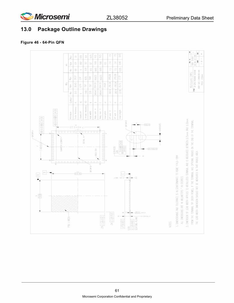
ZL38052 Preliminary Data Sheet
13.0 Package Outline Drawings
Figure 46 - 64-Pin QFN
61
Microsemi Corporation Confidential and Proprietary
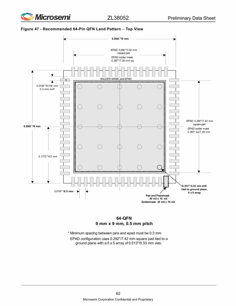
ZL38052 Preliminary Data Sheet
Figure 47 - Recommended 64-Pin QFN Land Pattern Top View
64-QFN9 mm x 9 mm, 0.5 mm pitch
EPAD configuration uses 0.292"/7.42 mm square pad tied to a ground plane with a 5 x 5 array of 0.013"/0.33 mm vias.
* Minimum spacing between pins and epad must be 0.3 mm
EPAD 0.292"/7.42 mm square pad
0.013"/0.33 mm drilltied to ground plane,
9 x 9 array0.0197 "/0.5 mm
0.1772 "/4.5 mm
Pad and Pastemask 30 mil x 10 mil
Soldermask 35 mil x 15 mil
SOLDER MASK and EPAD
0.3543 "/9 mm
1
0.0125 "/0.318 mm0.3 mm min*
EPAD solder mask 0.287" sq/7.29 mm
0.3543 "/9 mm
EPAD 0.292 "/7.42 mm square pad
EPAD solder mask 0.287"/7.29 mm sq
62
Microsemi Corporation Confidential and Proprietary

ZL38052 Preliminary Data Sheet
Figure 48 - 56-Ball WLCSP
63
Microsemi Corporation Confidential and Proprietary
Information relating to products and services furnished herein by Microsemi Corporation or its subsidiaries (collectively “Microsemi”) isbelieved to be reliable. However, Microsemi assumes no liability for errors that may appear in this publication, or for liability otherwisearising from the application or use of any such information, product or service or for any infringement of patents or other intellectualproperty rights owned by third parties which may result from such application or use. Neither the supply of such information or purchaseof product or service conveys any license, either express or implied, under patents or other intellectual property rights owned byMicrosemi or licensed from third parties by Microsemi, whatsoever. Purchasers of products are also hereby notified that the use ofproduct in certain ways or in combination with Microsemi, or non-Microsemi furnished goods or services may infringe patents or otherintellectual property rights owned by Microsemi.
This publication is issued to provide information only and (unless agreed by Microsemi in writing) may not be used, applied orreproduced for any purpose nor form part of any order or contract nor to be regarded as a representation relating to the products orservices concerned. The products, their specifications, services and other information appearing in this publication are subject tochange by Microsemi without notice. No warranty or guarantee express or implied is made regarding the capability, performance orsuitability of any product or service. Information concerning possible methods of use is provided as a guide only and does notconstitute any guarantee that such methods of use will be satisfactory in a specific piece of equipment. It is the user’s responsibility tofully determine the performance and suitability of any equipment using such information and to ensure that any publication or data usedis up to date and has not been superseded. Manufacturing does not necessarily include testing of all functions or parameters. Theseproducts are not suitable for use in any medical and other products whose failure to perform may result in significant injury or death tothe user. All products and materials are sold and services provided subject to Microsemi’s conditions of sale which are available onrequest.
For more information about all Microsemi productsvisit our website at
www.microsemi.com
TECHNICAL DOCUMENTATION – NOT FOR RESALE
© 2016 Microsemi Corporation. All rights reserved. Microsemi and the Microsemi logo are trademarks ofMicrosemi Corporation. All other trademarks and service marks are the property of their respective owners.
Microsemi Corporation (NASDAQ: MSCC) offers a comprehensive portfolio of semiconductorsolutions for: aerospace, defense and security; enterprise and communications; and industrialand alternative energy markets. Products include mixed-signal ICs, SoCs, and ASICs;programmable logic solutions; power management products; timing and voice processingdevices; RF solutions; discrete components; and systems. Microsemi is headquartered in AlisoViejo, Calif. Learn more at www.microsemi.com.
Microsemi Corporate HeadquartersOne Enterprise, Aliso Viejo CA 92656 USAWithin the USA: +1 (949) 380-6100Sales: +1 (949) 380-6136Fax: +1 (949) 215-4996