MT88E45B Data Sheet - Microsemi
30
1 Zarlink Semiconductor Inc. Zarlink, ZL and the Zarlink Semiconductor logo are trademarks of Zarlink Semiconductor Inc. Copyright 2001-2006, Zarlink Semiconductor Inc. All Rights Reserved. Features • Compatible with: • Bellcore GR-30-CORE, SR-TSV-002476, ANSI/TIA/EIA-716, TIA/EIA-777; • ETSI ETS 300 778-1 (FSK only variant) & -2; • BT (British Telecom) SIN227 & SIN242 • Bellcore ‘CPE Alerting Signal’ (CAS), ETSI ‘Dual Tone Alerting Signal’ (DT-AS), BT Idle State and Loop State ‘Tone Alert Signal’ detection • 1200 baud Bell 202 and CCITT V.23 FSK demodulation • Separate differential input amplifiers with adjustable gain for Tip/Ring and telephone hybrid or speech IC connections • Selectable 3-wire FSK data interface (bit stream or 1 byte buffer) • Facility to monitor the stop bit for framing error check • FSK Carrier detect status output • 3 to 5V +/- 10% supply voltage • Uses 3.579545 MHz crystal or ceramic resonator • Low power CMOS with power down Applications • Bellcore CID (Calling Identity Delivery) and CIDCW (Calling Identity Delivery on Call Waiting) telephones and adjuncts • ETSI, BT CLIP (Calling Line Identity Presentation) and CLIP with Call Waiting telephones and adjuncts • Fax and answering machines • Computer Telephony Integration (CTI) systems June 2006 Ordering Information MT88E45BN 20 Pin SSOP Tubes MT88E45BS 20 Pin SOIC Tubes MT88E45BSR 20 Pin SOIC Tape & Reel MT88E45BNR 20 Pin SSOP Tape & Reel MT88E45BN1 20 Pin SSOP* Tubes MT88E45BNR1 20 Pin SSOP* Tape & Reel, Bake & Drypack MT88E45BS1 20 Pin SOIC* Tubes, Bake & Drypack MT88E45BSR1 20 Pin SOIC* Tubes, Bake & Drypack *Pb Free Matte Tin -40°C to +85°C MT88E45 4-Wire Calling Number Identification Circuit 2 (4-Wire CNIC2) Data Sheet Figure 1 - Functional Block Diagram Anti-Alias Filter FSK Bandpass FSK Demodulator + - + - Data Timing Recovery Carrier Detector 2130Hz Bandpass 2750Hz Bandpass Tone Detection Algorithm FSKen+Tip/Ring CASen Hybrid CASen Guard Time Mux DR STD Bias Generator Oscillator Control Bit Decode FSKen CASen PWDN IN1+ IN1- GS1 IN2+ IN2- GS2 V REF OSC1 OSC2 CB0 CB2 CB1 DATA DCLK CD DR /STD ST/GT EST Vdd Vss MODE MODE FSKen CASen CASen PWDN PWDN PWDN PWDN
Transcript of MT88E45B Data Sheet - Microsemi

1Zarlink Semiconductor Inc.
Zarlink, ZL and the Zarlink Semiconductor logo are trademarks of Zarlink Semiconductor Inc.Copyright 2001-2006, Zarlink Semiconductor Inc. All Rights Reserved.
Features• Compatible with:
• Bellcore GR-30-CORE, SR-TSV-002476, ANSI/TIA/EIA-716, TIA/EIA-777;
• ETSI ETS 300 778-1 (FSK only variant) & -2;
• BT (British Telecom) SIN227 & SIN242
• Bellcore ‘CPE Alerting Signal’ (CAS), ETSI ‘Dual Tone Alerting Signal’ (DT-AS), BT Idle State and Loop State ‘Tone Alert Signal’ detection
• 1200 baud Bell 202 and CCITT V.23 FSK demodulation
• Separate differential input amplifiers with adjustable gain for Tip/Ring and telephone hybrid or speech IC connections
• Selectable 3-wire FSK data interface (bit stream or 1 byte buffer)
• Facility to monitor the stop bit for framing error check
• FSK Carrier detect status output
• 3 to 5V +/- 10% supply voltage
• Uses 3.579545 MHz crystal or ceramic resonator
• Low power CMOS with power down
Applications• Bellcore CID (Calling Identity Delivery) and
CIDCW (Calling Identity Delivery on Call Waiting) telephones and adjuncts
• ETSI, BT CLIP (Calling Line Identity Presentation) and CLIP with Call Waiting telephones and adjuncts
• Fax and answering machines
• Computer Telephony Integration (CTI) systems
June 2006
Ordering Information
MT88E45BN 20 Pin SSOP TubesMT88E45BS 20 Pin SOIC TubesMT88E45BSR 20 Pin SOIC Tape & ReelMT88E45BNR 20 Pin SSOP Tape & ReelMT88E45BN1 20 Pin SSOP* TubesMT88E45BNR1 20 Pin SSOP* Tape & Reel,
Bake & DrypackMT88E45BS1 20 Pin SOIC* Tubes, Bake & DrypackMT88E45BSR1 20 Pin SOIC* Tubes, Bake & Drypack
*Pb Free Matte Tin-40°C to +85°C
MT88E454-Wire Calling Number Identification
Circuit 2 (4-Wire CNIC2)Data Sheet
Figure 1 - Functional Block Diagram
Anti-AliasFilter
FSKBandpass
FSKDemodulator
+
-
+
-
Data TimingRecovery
CarrierDetector
2130HzBandpass
2750HzBandpass
ToneDetectionAlgorithm
FSKen+Tip/Ring CASen
Hybrid CASen
GuardTime
Mux
DR
STD
BiasGenerator
Oscillator
Control BitDecode
FSKen CASenPWDN
IN1+
IN1-
GS1
IN2+
IN2-
GS2
VREF
OSC1 OSC2 CB0 CB2CB1
DATA
DCLK
CD
DR/STD
ST/GT
EST
VddVss
MODE
MODE
FSKen
CASen
CASen
PWDN
PWDN
PWDN
PWDN

MT88E45 Data Sheet
2Zarlink Semiconductor Inc.
DescriptionThe MT88E45B is a low power CMOS integrated circuit suitable for receiving the physical layer signals used inNorth American (Bellcore) Calling Identity Delivery on Call Waiting (CIDCW) and Calling Identity Delivery (CID)services. It is also suitable for ETSI and BT Calling Line Identity Presentation (CLIP) and CLIP with Call Waitingservices.
The MT88E45B contains a 1200 baud Bell 202/CCITT V.23 FSK demodulator and a CAS/DT-AS detector. Twoinput op-amps allow the MT88E45B to be connected to both Tip/Ring and the telephone hybrid or speech ICreceive pair for optimal CIDCW telephone architectural implementation. FSK demodulation is always on Tip/Ring,while CAS detection can be on Tip/Ring or Hybrid Receive. Tip/Ring CAS detection is required for the Bellcore/TIAMultiple Extension Interworking (MEI) and BT’s on-hook CLIP. A selectable FSK data interface allows the data to beprocessed as a bit stream or extracted from a 1 byte on chip buffer. Power management has been incorporated topower down the FSK or CAS section when not required. Full chip power down is also available. The MT88E45B issuitable for applications using a fixed power source (with a +/-10% variation) between 3 and 5 V.
MT88E45 Data Sheet
3Zarlink Semiconductor Inc.
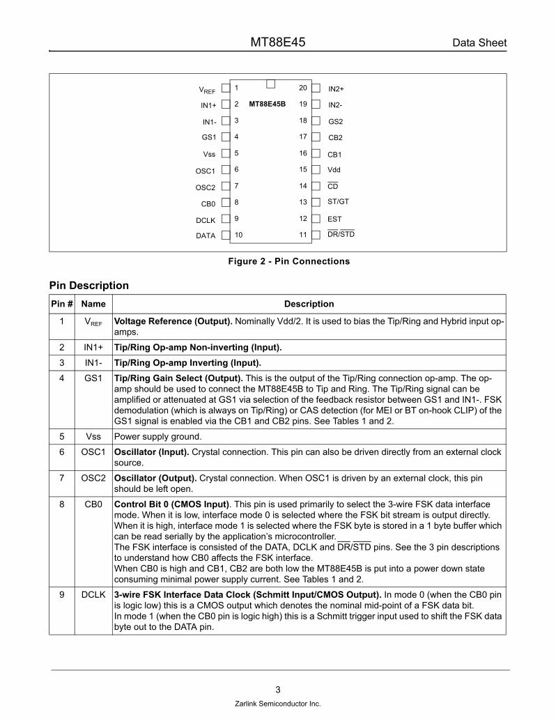
Figure 2 - Pin Connections
Pin DescriptionPin # Name Description
1 VREF Voltage Reference (Output). Nominally Vdd/2. It is used to bias the Tip/Ring and Hybrid input op-amps.
2 IN1+ Tip/Ring Op-amp Non-inverting (Input).3 IN1- Tip/Ring Op-amp Inverting (Input).4 GS1 Tip/Ring Gain Select (Output). This is the output of the Tip/Ring connection op-amp. The op-
amp should be used to connect the MT88E45B to Tip and Ring. The Tip/Ring signal can be amplified or attenuated at GS1 via selection of the feedback resistor between GS1 and IN1-. FSK demodulation (which is always on Tip/Ring) or CAS detection (for MEI or BT on-hook CLIP) of the GS1 signal is enabled via the CB1 and CB2 pins. See Tables 1 and 2.
5 Vss Power supply ground.
6 OSC1 Oscillator (Input). Crystal connection. This pin can also be driven directly from an external clock source.
7 OSC2 Oscillator (Output). Crystal connection. When OSC1 is driven by an external clock, this pin should be left open.
8 CB0 Control Bit 0 (CMOS Input). This pin is used primarily to select the 3-wire FSK data interface mode. When it is low, interface mode 0 is selected where the FSK bit stream is output directly. When it is high, interface mode 1 is selected where the FSK byte is stored in a 1 byte buffer which can be read serially by the application’s microcontroller.The FSK interface is consisted of the DATA, DCLK and DR/STD pins. See the 3 pin descriptions to understand how CB0 affects the FSK interface.When CB0 is high and CB1, CB2 are both low the MT88E45B is put into a power down state consuming minimal power supply current. See Tables 1 and 2.
9 DCLK 3-wire FSK Interface Data Clock (Schmitt Input/CMOS Output). In mode 0 (when the CB0 pin is logic low) this is a CMOS output which denotes the nominal mid-point of a FSK data bit. In mode 1 (when the CB0 pin is logic high) this is a Schmitt trigger input used to shift the FSK data byte out to the DATA pin.
1
2
3
4
5
6
9
10
20
19
18
17
16
15
14
13
VREF
IN1+
IN1-
GS1
Vss
OSC1
DCLK
DATA
IN2+
IN2-
GS2
CB2
CB1
Vdd
CD
ST/GT
MT88E45B
7OSC2
8CB0
12
11
EST
DR/STD
MT88E45 Data Sheet
4Zarlink Semiconductor Inc.
10 DATA 3-wire FSK Interface Data (CMOS Output). Mark frequency corresponds to logical 1. Spacefrequency corresponds to logical 0.In mode 0 (when the CB0 pin is logic low) the FSK serial bit stream is output to the DATA pindirectly. In mode 1 (when the CB0 pin is logic high) the start bit is stripped off, the data byte and the trailingstop bit are stored in a 9 bit buffer. At the end of each word signalled by the DR/STD pin, themicrocontroller should shift the byte out onto the DATA pin by applying 8 read pulses to the DCLKpin. A 9th DCLK pulse will shift out the stop bit for framing error checking.
11 DR/STD 3-wire FSK Interface Data Ready/CAS Detection Delayed Steering (CMOS Output). Activelow. When FSK demodulation is enabled via the CB1 and CB2 pins this pin is the Data Ready output.It denotes the end of a word. In both FSK interface modes 0 and 1, it is normally hi and goes lowfor half a bit time at the end of a word. But in mode 1 if DCLK starts during DR low, the first risingedge of the DCLK input will return DR to high. This feature allows an interrupt requested by a lowgoing DR to be cleared upon reading the first DATA bit. When CAS detection is enabled via the CB1 and CB2 pins this pin is the Delayed Steering output.It goes low to indicate that a time qualified CAS has been detected.
12 EST CAS Detection Early Steering (CMOS Output). Active high. This pin is the raw CAS detectionoutput. It goes high to indicate the presence of a signal meeting the CAS accept frequencies andsignal level. It is used in conjunction with the ST/GT pin and external components to time qualifythe detection to determine whether the signal is a real CAS.
13 ST/GT CAS Detection Steering/Guard Time (CMOS Output/Analog Input). It is used in conjunctionwith the EST pin and external components to time qualify the detection to determine whether thesignal is a real CAS. A voltage greater than VTGt at this pin causes the MT88E45B to indicate that a CAS has beendetected by asserting the DR/STD pin low. A voltage less than VTGt frees up the MT88E45B toaccept a new CAS and returns DR/STD to high.
14 CD Carrier Detect (CMOS Output). Active low. A logic low indicates that an FSK signal is present. A time hysteresis is provided to allow formomentary signal discontinuity. The demodulated FSK data is ignored by the MT88E45B untilcarrier detect has been activated.
15 Vdd Positive power supply.
16 CB1 Control Bit 1 (CMOS Input). Together with CB2 this pin selects the MT88E45B’s functionalitybetween FSK demodulation, Tip/Ring CAS detection and Hybrid CAS detection. When CB0 is high and CB1, CB2 are both low the MT88E45B is put into a power down stateconsuming minimal power supply current. See Tables 1 and 2.
17 CB2 Control Bit 2 (CMOS Input). Together with CB1 this pin selects the MT88E45B’s functionalitybetween FSK demodulation, Tip/Ring CAS detection and Hybrid CAS detection. When CB0 is high and CB1, CB2 are both low the MT88E45B is put into a power down stateconsuming minimal power supply current. See Tables 1 and 2.
18 GS2 Hybrid Gain Select (Output). This is the output of the hybrid receive connection op-amp. The op-amp should be used to connect the MT88E45B to the telephone hybrid or speech IC receive pair.The hybrid receive signal can be amplified or attenuated at GS2 via selection of the feedbackresistor between GS2 and IN2-. When the CPE is off-hook CAS detection of the GS2 signalshould be enabled via the CB1 and CB2 pins. See Tables 1 and 2.
19 IN2- Hybrid Op-amp Inverting (Input).20 IN2+ Hybrid Op-amp Non-Inverting (Input).
Pin DescriptionPin # Name Description

MT88E45 Data Sheet
5Zarlink Semiconductor Inc.
Table 1 - CB0/1/2 Functionality
The number of control bits (CB) required to interface the MT88E45B with the microcontroller depends on thefunctionality of the application, as shown in Table 2.
Table 2 - Control Bit Functionality Groups
Functional OverviewThe MT88E45B is compatible with FSK and FSK plus CAS (CPE Alerting Signal) based Caller ID services aroundthe world. Caller ID is the generic name for a group of services offered by telephone operating companies wherebyinformation about the calling party is delivered to the subscriber. In Europe and some other countries Caller ID isknown as Calling Line Identity Presentation (CLIP). ETSI calls CAS ‘Dual Tone Alerting Signal’ (DT-AS), BT calls it‘Tone Alert Signal’.
Depending on the service, data delivery can occur when the line is in the on-hook or off-hook state. In mostcountries the data is modulated in either Bell 202 or CCITT V.23 FSK format and transmitted at 1200 baud from theserving end office to the subscriber’s terminal. Additionally in off-hook signalling, the special dual tone CAS is used
CB0 CB1 CB2 FSK Interface Function
0/1 1 1 Set by CB0 FSK Demodulation. Tip/Ring input (GS1) selected. DR/STD is DR.
0/1 1 0 Set by CB0 Hybrid CAS Detection. Hybrid Receive input (GS2) selected. DR/STD is STD.
0/1 0 1 Set by CB0 Tip/Ring CAS Detection. Tip/Ring input (GS1) selected. DR/STD is STD.When the line is off-hook, a Bellcore/TIA Multiple Extension Interworking (MEI) compatible Type 2 CPE should be able to detect CAS from Tip/Ring while the CPE is on-hook because it may be the ACK sender. Tip/Ring CAS detection is also required for BT’s on-hook CLIP.
1 0 0 Mode 1 Power Down. The MT88E45B is disabled and draws virtually no power supply current.
0 0 0 Mode 0 Reserved for factory testing.
Functionality Group Controls Description
FSK (mode 0 or 1) and Hybrid CAS only(Non MEI compatible)
CB2 CB0 is hardwired to Vdd or Vss to select the FSK interface.CB1 hardwired to Vdd.The microcontroller uses CB2 to select between the 2 functions.
FSK (mode 0 or 1), Hybrid CAS,Tip/Ring CAS(MEI compatible or BT on-hook CLIP)
CB1CB2
CB0 is hardwired to Vdd or Vss to select the FSK interface.The microcontroller uses CB1 and CB2 to select between the 3 functions.
FSK (mode 1), Hybrid CAS, Tip/Ring CAS, Power Down(MEI compatible or BT on-hook CLIP)
CB1CB2
CB0 is hardwired to Vdd to select FSK interface mode 1.The microcontroller uses CB1 and CB2 to select between the 4 functions.
FSK (mode 0), Hybrid CAS,Tip/Ring CAS, Power Down(MEI compatible or BT on-hook CLIP)
CB0CB1CB2
All 3 pins are required.

MT88E45 Data Sheet
6Zarlink Semiconductor Inc.
to alert the terminal before FSK data transmission. BT uses CAS to alert the terminal prior to FSK in both on-hook(Idle State) and off-hook (Loop State) signalling.
In North America, Caller ID uses the voiceband data transmission interface defined in the Bellcore document GR-30-CORE. The terminal or CPE (Customer Premises Equipment) requirements are defined in Bellcore documentSR-TSV-002476. Typical services are CND (Calling Number Delivery), CNAM (Calling Name Delivery), VMWI(Visual Message Waiting Indicator) and CIDCW (Calling Identity Delivery on Call Waiting).
In Europe, Caller ID requirements are defined by ETSI. The CPE documents are ETS 300 778-1 for on-hook, ETS300 778-2 for off-hook. The end office requirements are ETS 300 659-1 (on-hook) and ETS 300 659-2 (off-hook).ETSI has defined services such as CLIP and CLIP with Call Waiting which are similar to those of Bellcore. SomeEuropean countries produce their own national specifications. For example, in the UK BT’s standards are SIN227and SIN242, the UK CCA (Cable Communications Association) standard is TW/P&E/312.
In on-hook Caller ID, such as CND, CNAM and CLIP, the information is typically transmitted (in FSK) from the endoffice before the subscriber picks up the phone. There are various methods such as between the first and secondrings (North America), between an abbreviated ring and the first true ring (Japan, France and Germany). On-hookCaller ID can also occur without ringing for services such as VMWI. In BT’s on-hook CLIP, the signalling begins witha line polarity reversal, followed by CAS and then FSK. Bellcore calls an on-hook capable Caller ID CPE a ‘Type 1CPE’.
In off-hook Caller ID, such as CIDCW and CLIP with Call Waiting, information about a new calling party is sent tothe subscriber who is already engaged in a call. Bellcore’s method uses CAS to alert the CPE. When the CPEdetects CAS and there are no off-hook extensions, the CPE should mute its transmission path and send anacknowledgment to the end office via a DTMF digit called ACK. Upon receiving ACK, the end office will send theFSK data. Bellcore calls an off-hook capable CPE a ‘Type 2 CPE’. A Type 2 CPE is capable of off-hook and Type 1functionalities and should ACK with a DTMF ‘D’. The ETSI and BT off-hook signalling protocols are similar toBellcore’s but with timing and signal parametric differences. ETSI has no requirement for off-hook extensionchecking before ACK.
One factor affecting the quality of the CIDCW service is the CPE’s CAS speech immunity. Although the end officehas muted the far end party before and after it sends CAS, the near end (the end which is to receive theinformation) user may be still talking. Therefore the CPE must be able to detect CAS successfully in the presenceof near end speech. This is called the talkdown immunity. The CPE must also be immune to imitation of CAS byspeech from both ends of the connection because the CAS detector is continuously exposed to speech throughoutthe call. This is called the talkoff immunity.
If the CPE is a telephone, one way to achieve good CAS speech immunity is to put CAS detection on the telephonehybrid or speech IC receive pair instead of on Tip and Ring. Talkdown immunity improves because the near endspeech has been attenuated while the CAS level is the same as on Tip/Ring, resulting in improved signal to speechratio. Talkoff immunity is also improved because the near end speech has been attenuated.
In the Bellcore SR-TSV-002476 Issue 1 off-hook protocol, the CPE should not ACK if it detected an off-hookextension. The FSK will not be sent and the customer will not receive the Call Waiting ID. Bellcore, together with theTIA (Telecommunications Industry Association) TR41.3.1 working group, has defined a CPE capability calledMultiple Extension Interworking (MEI) which overcomes this problem.
In the MEI scheme, all MEI compatible CPEs must be capable of detecting CAS when the line is off-hook, eventhough the CPE itself may be on-hook. This is because under some conditions an on-hook CPE may become theACK sender. Another reason for the on-hook CPE to detect CAS is to maintain synchronous call logs between onand off-hook CPEs. When CAS is received and all off-hook CPEs are MEI compatible, one of the CPEs will ACKand all compatible CPEs will receive FSK.
A problem arises in a CPE where the CAS detector is connected only to the hybrid or speech IC receive pair: itcannot detect CAS when it is on-hook. The reason is that when the CPE is on-hook either the hybrid/speech IC isnon functional or the signal level is severely attenuated. Therefore an on-hook Type 2 CPE must be capable of

MT88E45 Data Sheet
7Zarlink Semiconductor Inc.
detecting CAS from Tip/Ring, in addition to detecting CAS from the hybrid/speech IC receive signal when it is off-hook.
The MT88E45B offers an optimal solution which combines good speech immunity and MEI compatibility. Two inputop-amps allow the MT88E45B to be connected both to Tip/Ring and to the hybrid/speech IC receive pair. Bothconnections can be differential or single ended. FSK demodulation is always on the Tip/Ring signal. CAS detectioncan be from the Tip/Ring or hybrid/speech IC receive signal. Being able to detect CAS on Tip/Ring also makes theMT88E45B suitable for BT on-hook CLIP applications.
For applications such as those in most European countries where Tip/Ring CAS detection is not needed, then theTip/Ring and Hybrid op-amp gains can be tailored independently to meet country specific FSK and CAS signal levelrequirements respectively. Note that since the Hybrid op-amp is for CAS detection only, its gain can always betailored specifically for the CAS signal level.
The FSK demodulator is compatible with Bellcore, ETSI and BT standards. The demodulated FSK data is eitheroutput directly (bit stream mode) or stored in a one byte buffer (buffer mode). In the buffer mode, the stop bitimmediately following a byte is also stored and can be shifted out after the data byte. This facility allows for framingerror checking required in Type 2 CPEs. In the bit stream mode, two timing signals are provided. One indicates thebit sampling instants of the data byte, the other the end of byte. A carrier detector indicates presence of signal andshuts off the data stream when there is no signal.
The entire chip can be put into a virtually zero current power down mode. The input op-amps, FSK demodulator,CAS detector and the oscillator are all shut off. Furthermore, power management has been incorporated tominimize operating current. When FSK is selected the CAS detector is powered down. When CAS is selected theFSK demodulator is powered down.
Functional Description
3 to 5 V Operation
The MT88E45B’s FSK and CAS reject levels are proportional to Vdd. When operated at Vdd equal 3 V +/- 10%, tokeep the FSK and CAS reject levels as at 5 V (nominal) the Tip/Ring and Hybrid op-amp gains should be reducedfrom those of 5 V. Gains for nominal Vdd (with a +/- 10% variation) other than 3 or 5 V can be chosen asinterpolation between the 3 and 5 V settings.
Input Configuration
The MT88E45B provides an input arrangement comprised of two op-amps and a bias source (VREF). VREF is a lowimpedance voltage source which is used to bias the op-amp inputs at Vdd/2. The Tip/Ring op-amp (IN1+, IN1-, GS1pins) is for connecting to Tip and Ring. The Hybrid op-amp (IN2+, IN2-, GS2 pins) is for connecting to the telephonehybrid or speech IC receive pair.
Either FSK or CAS detection can be selected for the Tip/Ring connection, while the hybrid connection is for CASdetection only. Phrased in another way, FSK demodulation is always on Tip/Ring, while CAS detection can be onTip/Ring or Hybrid Receive. Tip/Ring CAS detection is required for MEI and BT on-hook CLIP, while Hybrid CASdetection is needed for optimal CAS speech immunity.
The feedback resistor connected between GS1 and IN1- can be used to adjust the Tip/Ring signal gain. Thefeedback resistor connected between GS2 and IN2- can be used to adjust the hybrid receive signal gain. When theTip/Ring op-amp is selected, the GS2 signal is ignored. When the Hybrid op-amp is selected, the GS1 signal isignored.
Either or both op-amps can be configured in the single ended input configuration shown in Figure 33, or in thedifferential input configuration shown in Figure 44.

MT88E45 Data Sheet
8Zarlink Semiconductor Inc.
Figure 3 - Single Ended Input Configuration
Figure 4 - Differential Input Configuration
CAS Detection
In North America, CAS is used in off-hook signalling only. In Europe (ETSI) it is used in off-hook signalling, and byBT in both on and off-hook signalling. ETSI calls it the Dual Tone Alerting Signal (DT-AS). Although the ETSI on-hook standard contains a DT-AS specification, BT is the only administration known to employ CAS in on-hooksignalling. (BT calls it Tone Alert Signal.) The CAS/DT-AS characteristics are summarized in Table 3.
2130 Hz and 2750 Hz CAS/DT-AS Characteristics
Bellcorea
(Off-hook only)ETSIb
(Off-hook)BTc
(Off-hook = ‘Loop State’)(On-hook = ‘Idle State’)
Frequency Tolerance +/-0.5% +/-0.5% Off-hook: +/-0.6%On-hook: +/-1.1%
Signal Level (per tone) -14 to -32 dBmd -9.78 to -32.78 dBm(-12 to -35 dBVe)
+0.22 to -37.78 dBm(-2 to -40 dBV)
Reject Level (per tone) -45 dBm On-hook: -43.78 dBm(-46 dBV)
Maximum Twist (V2130Hz/V2750Hz) +/-6 dB +/-6 dB +/-7 dB
C RIN
IN+
IN-
GS
Highpass Corner Frequencyf-3dB = 1/(2πRINC)
RF Voltage Gain (AV) = RF / RIN VREF
C1 R1
C2 R4
R3 R2
R5
IN+
IN-
GS
VREFDifferential Input AmplifierC1 = C2R1 = R4 (For unity gain R5= R4)R3 = (R2R5) / (R2 + R5)Voltage Gain(AVdiff) = R5/R1
Input Impedance(ZINdiff) = 2 R12 + (1/ωC)2
Highpass Corner Frequencyf-3dB = 1/(2πR1C1)

MT88E45 Data Sheet
9Zarlink Semiconductor Inc.
Table 3 - CAS/DT-AS Characteristics
Table 3 shows the Hybrid op-amp (GS2) gain for operation at 3 V and 5 V nominal Vdd, with a ± 10% Vdd variation.For 3 V operation, the Hybrid op-amp gain should be reduced from the 5 V setting to maintain the CAS reject leveland to maintain the talkoff immunity: the CAS threshold is directly proportional to Vdd, when Vdd is reduced thethreshold becomes lower, hence lower level CAS are accepted. If the gain is not reduced, the MT88E45B will bemore talkoff prone. In Table 3, the GS2 gain is shown as a range. By adopting the lower gain, talkoff immunity canbe improved.
When CAS detection is selected, the dual purpose output pin DR/STD is STD. STD goes low when CAS has beendetected, and returns high after CAS has ended.
CAS Guard Time
The guard time circuit shown in Figure 55 implements a timing algorithm which determines whether the signal is aCAS. Proper selection of the guard time(s) is key to good speech immunity. The first indication that there might be aCAS is when EST goes high. EST high indicates that both tones are present. EST low indicates that one or bothtones is not present. STD low indicates that CAS has been detected. When STD returns high it indicates that CAShas ended.
The timing algorithm consists of 2 components: a tone present guard time (tGP) and a tone absent guard time (tGA).tGP sets the minimum accept duration for CAS. That is, both tones must be detected continuously for tGP for STD togo low to indicate that CAS has been detected. For STD to return high to indicate that CAS has ended, one or bothtones must have disappeared for tGA. The purpose of tGA is to bridge over momentary EST dropouts once EST hasmet the minimum tone duration so as to decrease the likelihood of a long talkoff being broken up into severaltalkoffs. Usually tGA is set very short or removed altogether because there is another way to deal with the problem(by ignoring further detections for 2 seconds after every detection).
Duration 75 to 85 ms 75 to 85 ms Off-hook: 80 to 85 msOn-hook: 88 to 110 ms
Reject Duration Off-hook: <=70 msOn-hook: <=20 ms
Signal to Noise Ratio Speech Speech Off-hook: SpeechOn-hook: >= 20 dB
(300-3400 Hz)Hybrid Op-amp (GS2) GainVdd = 5V +/- 10%
0 to -5 dB 0 to -5 dB 0 dB
Hybrid Op-amp (GS2) GainVdd = 3V +/- 10%
-3.5 to -8.5 dB -3.5 to -8.5 dB -3.5 dB
a. SR-TSV-002476, Issue 1 Dec 1992b. ETS 300 778-2 Jan 98. The DT-AS plus FSK variant of ETSI on-hook signalling described in ETS 300 778-1 is not supported
because on-hook DT-AS uses the GS1 op-amp. With the GS1 gain in Table 4, the DT-AS minimum level will be below the MT88E45B’s minimum accept level.
c. SIN227 Issue 3 Nov 97, SIN242 Issue 2 Nov 96d. dBm - Decibels above or below a reference power of 1 mW into 600 ohms. 0 dBm = 0.7746 Vrms.e. dBV - Decibels above or below a reference voltage of 1 Vrms. 0 dBV = 1 Vrms
2130 Hz and 2750 Hz CAS/DT-AS Characteristics
Bellcorea
(Off-hook only)ETSIb
(Off-hook)BTc
(Off-hook = ‘Loop State’)(On-hook = ‘Idle State’)

MT88E45 Data Sheet
10Zarlink Semiconductor Inc.
Figure 5 - CAS Guard Time Circuit Operation
Tone present guard time (tGP) operation: In Figure 5 5 initially there is no CAS, EST is low so Q1 is off. C has beenfully charged applying 0 V to ST/GT so Q2 is on. When both tones are detected EST goes high and turns off Q2.Because C has been fully charged (ST/GT=0V), the comparator output is low and Q1 stays off. With both Q1 andQ2 off the high at EST discharges C through R1 and the ST/GT voltage increases from 0 V. When the voltageexceeds the comparator threshold VTGt, which is typically 0.5 Vdd, the comparator output goes high; Q1 turns onand accelerates the discharge of C (ST/GT goes quickly to Vdd); STD goes low to indicate that a valid CAS hasbeen received. If one or both tones disappeared before tGP has been reached (i.e. when ST/GT voltage is still belowVTGt), Q2 turns back on and charges C quickly to bring the ST/GT voltage back to 0 V. Then if EST goes high againthe tGP duration must start over.
Tone absent guard time (tGA) operation: In Figure 5 5 initially both tones have been detected for tGP so C is fullydischarged and ST/GT is at Vdd. While both tones continue to be detected EST stays high; ST/GT is at Vdd (thecomparator output is high); so Q1 is on and Q2 is off. When one or both tones stop EST goes low and turns off Q1.Because C is fully discharged (ST/GT=Vdd), the comparator output is high and Q2 stays off. With both Q1 and Q2off the low at EST charges C through Rp=(R1 || R2) and the ST/GT voltage falls towards 0V. When the voltage hasfallen below VTGt, the comparator output goes low. Since EST is also low Q2 turns on and accelerates thecharging of C so that ST/GT goes quickly to 0V. STD goes high to indicate that the CAS has ended. If EST goesback to high before tGA has been reached (i.e. when ST/GT voltage is still above VTGt), Q1 turns back on anddischarges C quickly to bring the ST/GT voltage back to Vdd. Then if EST goes low again the tGA duration must startover. To set tGA=0, set R2 to 0.
+
- VTGt
EST
ST/GT
Vdd
DR/STD
= Vss
Both Tones PresentCQ1
Q2
MT88E45B
Comparator
P
N
CAS
EST
ST/GT
STD
tDP tDA
tGAtGP
R1 R2
Rp=R1 || R2
tABStREC
Indicates STD in CASdetection mode
tGP=R1C ln [Vdd / (Vdd-VTGt)]
tGA=RpC ln Vdd - Vdiode (Rp/R2) VTGt - Vdiode (Rp/R2)
Rp=R1 || R2
tGA=0 if R2=0
Vdiode

MT88E45 Data Sheet
11Zarlink Semiconductor Inc.
In Figure 55, tDP is the delay from the start of CAS to EST responding, tDA is the delay from the end of CAS to ESTresponding. The total delay from the start of CAS to STD responding is tREC=tDP+tGP. The total delay from the end ofCAS to STD responding is tABS=tDA+tGA.
Table 4 - FSK Signal Characteristics
FSK DemodulationThe FSK characteristics are shown in Table 4. In North America, TIA (Telecommunications Industry Association)also sets standards. The Type 1 Caller ID CPE standard is ANSI/TIA/EIA-716. The Type 2 standard is TIA/EIA-777.The North American FSK characteristics in Table 4 are from ANSI/TIA/EIA-716. They differ from those Bellcorepublished in SR-TSV-002476 and SR-3004. Bellcore is represented in TR41.3.1 and will synchronize to the TIArequirements in its future documents.
The TIA Type 1 standard includes an FSK reject level:
• if data is not preceded by ringing (e.g., VMWI), FSK signals below 3mVrms (-48.24 dBm) shall be rejected
• if data is preceded by ringing, FSK detection may be extended below 3mVrms
The MT88E45B is compliant with the Bellcore/TIA, ETSI and BT requirements with the Tip/Ring op-amp gains inTable 4. In Europe if the country specific FSK requirements do not incorporate ETSI’s FSK reject level then theTip/Ring op-amp gain can also be 0 dB at 5 V and -3.5 dB at 3 V to meet the ETSI minimum CAS level for on-hooksignalling (-40 dBV).
Parameter North America: Bellcorea Europe: ETSIb UK: BTc
Mark (Logical 1) Frequency 1200 Hz +/- 1% 1300 Hz +/- 1.5%
Space (Logical 0) Frequency 2200 Hz +/- 1% 2100 Hz +/- 1.5%
Received Signal Level -4.23 to -36.20 dBm(476 to 12 mVrms)d
-5.78 to -33.78 dBme
(-8 to -36 dBV)f,g-5.78 to -37.78 dBm
(-8 to -40 dBV)
Signal Reject Level -48.24 dBm (3mVrms) for On-hook No Ring Signalling
such as VMWI
On-hook only:-47.78 dBm
(-50dBV)
Transmission Rate 1200 baud +/- 1% 1200 baud +/- 1%
Twist (VMARK/VSPACE) -6 to +10 dB -6 to +6 dB
Signal to Noise Ratio Single Tone (f):-18 dB (f<=60Hz)
-12 dB (60<f<=120Hz)-6 dB (120<f<=200Hz)
+25 dB (200<f<3200Hz)+6 dB (f>=3200Hz)
>= 25 dB(300 to 3400 Hz)
>= 20 dB(300 to 3400 Hz)
Tip/Ring Op-Amp (GS1) GainVdd = 5V +/- 10%
0 dB -2 dBh 0 dB
Tip/Ring Op-Amp (GS1) GainVdd = 3V +/- 10%
-3.5 dB -5.5 dBi -3.5 dB
a. ANSI/TIA/EIA-716 and TIA/EIA-777. Bellcore has agreed to the values and will synchronize its requirements.b. ETS 300 778-1 (On-hook) Sep 97, ETS 300 778-2 (Off-hook) Jan 98.c. SIN 227 Issue 3 Nov 97, SIN242 Issue 2 Nov 96.d. North American on-hook signalling range. The off-hook range is inside the on-hook range: 190mVrms to 12mVrms.e. dBm - Decibels above or below a reference power of 1 mW into 600 ohms. 0 dBm = 0.7746 Vrmsf. dBV - Decibels above or below a reference voltage of 1 Vrms. 0 dBV = 1 Vrms.g. ETSI on-hook signalling range. The off-Hook signalling levels are inside this range: -8.78 to -30.78 dBm (-11 to -33 dBV).h. The 5V ETSI Tip/Ring op-amp gain can be 0 dB if there is no FSK reject level requirement.i. The 3V ETSI Tip/Ring op-amp gain can be -3.5dB if there is no FSK reject level requirement.

MT88E45 Data Sheet
12Zarlink Semiconductor Inc.
For 3 V operation, the FSK receiver becomes more sensitive and lower level signals will be accepted than at 5 V. Tomaintain the FSK reject level, the Tip/Ring input op-amp gain should be reduced. Note that since the Tip/Ring op-amp is also used for Tip/Ring CAS detection, the CAS level will also be reduced for on-hook detection.
FSK Data InterfaceThe MT88E45B provides a powerful dual mode 3-wire interface so that the data bytes in the demodulated FSK bitstream can be extracted without the need either for an external UART or for the CPE’s microcontroller to performthe function in software. The interface is specifically designed for the 1200 baud rate and is consisted of 3 pins:DATA, DCLK (Data Clock) and DR (Data Ready). DR/STD is a dual purpose output pin. When FSK is selected it isDR.
Two modes (modes 0 and 1) are selectable via the CB0 pin. In mode 0, the FSK bit stream is output directly. Inmode 1, the data byte and the trailing stop bit are stored in a 9 bit buffer. If mode 1 is desired, the CB0 pin can behardwired to Vdd. If mode 0 is desired and full chip power down is not required, the CB0 pin can be hardwired toVss.
In Bellcore’s off-hook protocol, a Type 2 CPE should restore the voicepath within 50 ms after the end of the FSKsignal. Due to noise, end of carrier detection is not always reliable. The TIA Type 2 standard stipulates that the CPEmust detect the end of FSK when any one of the following occurs:
• absence of carrier signal or,
• more than five framing errors (trailing stop bit a 0 instead of a 1) have been detected in the FSK message or,
• more than 150 ms of continuous mark signal or space signal has been detected.
Mode 0 - Bit Stream Mode
This mode is selected when the CB0 pin is low. In this mode the FSK data is output directly to the DATA pin. DCLKand DR pins are timing signal outputs (see Figure 13.
For each received stop and start bit sequence, the MT88E45B outputs a fixed frequency clock string of 8 pulses atthe DCLK pin. Each DCLK rising edge occurs in the middle of a DATA bit cell. DCLK is not generated for the startand stop bits. Consequently, DCLK will clock only valid data into a peripheral device such as a serial to parallel shiftregister or a microcontroller. The MT88E45B also outputs an end of word pulse (Data Ready) at the DR pin. DRgoes low for half a nominal bit time at the beginning of the trailing stop bit. It can be used to interrupt amicrocontroller or cause a serial to parallel converter to parallel load its data into the microcontroller. Since the DRrising edge occurs in the middle of the stop bit, it can also be used to read the stop bit to check for framing error.
Alternatively, DCLK and DATA may occupy 2 bits of a microcontroller’s input port. The microcontroller polls theinput port and saves the DATA bit whenever DCLK changes from low to high. When DR goes low, the word maythen be assembled from the last 8 saved bits.
DATA may also be connected to a personal computer’s serial communication port after conversion from CMOS toRS-232 voltage levels.
Mode 1 - Buffer Mode
This mode is selected when the CB0 pin is high. In this mode the received byte is stored on chip. At the end of abyte DR goes low to indicate that a new byte has become available. The microcontroller applies DCLK pulses toread the register contents serially out of the DATA pin (see Figure 1414).
Internal to the MT88E45B, the start bit is stripped off, the data bits and the trailing stop bit are sampled and stored.Midway through the stop bit, the 8 data bits and the stop bit are parallel loaded into a 9 bit shift register and DRgoes low. The register’s contents are shifted out to the DATA pin on the supplied DCLK’s rising edges in the orderthey were received. The last bit must be shifted out and DCLK returned to low before the next DR. DCLK must below for tDDS before DR goes low and must remain low for tDDH after DR has gone low (see Figure 14).

MT88E45 Data Sheet
13Zarlink Semiconductor Inc.
If DCLK begins while DR is low, DR will return to high upon the first DCLK rising edge. If DR interrupts amicrocontroller then this feature allows the interrupt to be cleared by the first read pulse. Otherwise DR is low forhalf a nominal bit time (1/2400 sec).
Reading the stop bit allows the software to check for framing errors. When framing error is not checked themicrocontroller only needs to send 8 DCLK pulses to shift the data byte out.
Carrier DetectThe carrier detector provides an indication of the presence of a signal in the FSK frequency band. It detects thepresence of a signal of sufficient amplitude at the output of the FSK bandpass filter. The signal is qualified by afrequency aware digital algorithm before the CD output is set low to indicate carrier detection. A 10 ms hysteresis isprovided to allow for momentary signal dropout once CD has been activated. CD is released when there is noactivity at the FSK bandpass filter output for 10 ms.
When CD is inactive (high), the raw output of the FSK demodulator is ignored by the internal data timing recoverycircuit. In mode 0 the DATA, DCLK and DR pins are forced high. In mode 1 the output shift register is not updatedand DR is high; if DCLK is clocked, DATA is undefined.
Note that signals such as speech, CAS and DTMF tones also lie in the FSK frequency band and the carrier detectormay be activated by these signals. They will be demodulated and presented as data. To avoid the false data, theMT88E45B should be put into CAS or power down mode when FSK is not expected. Ringing, on the other hand,does not pose a problem as it is ignored by the carrier detector.
InterruptThe DR/STD output can be used to interrupt a microcontroller. When the MT88E45B is the only interrupt source,DR/STD can be connected directly to the microcontroller’s interrupt input. Figure 9 shows the necessaryconnections when the MT88E45B is one of many interrupt sources. The diodes and resistors implement a wired-orso that the microcontroller is interrupted (INT low active or falling edge triggered) when one or more of INT1, INT2or DR/STD is low. The microcontroller can determine which one of DR/STD, INT1 or INT2 caused the interrupt byreading them into an input port.
When system power is first applied and CB0/1/2 have already been configured to select CAS detection, DR/STDwill power up as logic low. This is because there is no charge across the ST/GT capacitor in Figure 55, henceST/GT is at Vdd which causes STD to be low. If DR/STD is used to interrupt a microcontroller the interrupt will notclear until the capacitor has charged up. Therefore upon initial power up the microcontroller should ignore thisinterrupt source until there is sufficient time to charge the capacitor. Alternatively, the MT88E45B can be put intopower down mode: DR/STD goes high and clears the interrupt, ST/GT goes low and the capacitor will charge upquickly.
Power DownThe MT88E45B can be powered down to consume virtually no power supply current via a state of the CB0/1/2 pins.Momentary transition of CB0/1/2 into the power down code will not activate power down.
In power down mode both input op-amps, VREF and the oscillator are non functional. DCLK becomes an inputbecause to select the power down state CB0 is 1 which will select FSK interface mode 1. If the application usesFSK interface mode 0 and the MT88E45B needs to be powered down then a pull down resistor should be addedat the DCLK pin to define its state during power down (R15 in Figure 7). When the MT88E45B is powered downDATA, DR/STD, CD are high; EST and ST/GT are low.
To reduce the operating current an Intelligent Power Down feature has been incorporated. When FSK is selected,the CAS detector is powered down. When CAS is selected the FSK demodulator is powered down. The two inputop-amps are not affected and both will remain operational.

MT88E45 Data Sheet
14Zarlink Semiconductor Inc.
OscillatorThe MT88E45B requires a 3.579545 MHz crystal or ceramic resonator to generate its oscillator clock. To meet theCAS detection frequency tolerance specifications the crystal or resonator must have a 0.1% frequency tolerance.The crystal specification is as follows: (e.g., CTS MP036S)
Frequency: 3.579545 MHzFrequency Tolerance: ± 0.1% (over temperature
range of the application)Resonance Mode: ParallelLoad Capacitance: 18 pFMaximum Series Resistance: 150 ΩMaximum Drive Level: 2 mW
Alternatively an external clock source can be used. In which case the OSC1 pin should be driven directly from aCMOS buffer and the OSC2 pin left open.
For 5V+/-10% applications any number of MT88E45B’s can be connected as shown in Figure 6 6 so that only onecrystal is required.
Figure 6 - Common Crystal Connection
OSC1 OSC2 OSC1 OSC2 OSC1 OSC2
3.579545 MHz
MT88E45B MT88E45B MT88E45B
to the next MT88E45B
(For 5V+/-10% applications only)

MT88E45 Data Sheet
15Zarlink Semiconductor Inc.
Application Circuits
Figure 7 - Application Circuit: Bellcore MEI Compatible Type 2 Telephone
VREF
IN1+
IN1-
GS1
Vss
OSC1
DCLK
DATA
IN2+
IN2-
GS2
CB2
CB1
Vdd
CD
ST/GT
MT88E45B
OSC2
CB0
EST
DR/STD
Telephone
Tx+
Tx-
Rx+
Rx-
TIP
RING
Microphone
Speaker
TIP
RING
R1
R2
R3
R4
R5 R6
D1
D2
D3
D4
R7
R8
R9
R10R11
R12
R13
R14
D5
C1
C2
C3
C4
Xtal
R15
C5 C6
Hybridor
(FSK Interface Mode 1 selected)
R15 is required only if both FSK interface mode 0 and power down features are used.
C6 should be connected directly across Vdd and Vss pins
Unless stated otherwise, resistors are 1%, 0.1Watt; capacitors are 5%, 6.3V.
For 1000Vrms, 60Hz isolation from Tip to Earth and Ring to Earth:R1,R2 430K, 0.5W, 5%, 475V min. C1,C2 2n2, 1332V min.
(e.g. IRC type GS-3)
If the 1000Vrms is handled by other methods then this circuit has to meet the FCC Part 68 Type B Ringer requirements:R1,R2 432K, 0.1W, 1%, 56V min. C1,C2 2n2, 212V min.
Common to both sets of R1,R2: 5V, 0dB gain 3V, -3.5dB gainR3,R4 34K C3,C4 2n2 R5,R10 53K6 35K7R8,R9 464K C5 100n R6,R11 60K4 40K2R13 825K C6 100n, 20% R7,R12 464K 309KR14 226K or 26K1 D1-D4 Diodes. 1N4148 or equivalentR15 100K, 20% D5 Diode. 1N4148 or equivalent
Xtal 3.579545MHz, 0.1% crystalor ceramic resonator
Vdd= To Microcontroller
= From Microcontroller Vss
Speech IC(Symbolic)
MT88E45 Data Sheet
16Zarlink Semiconductor Inc.
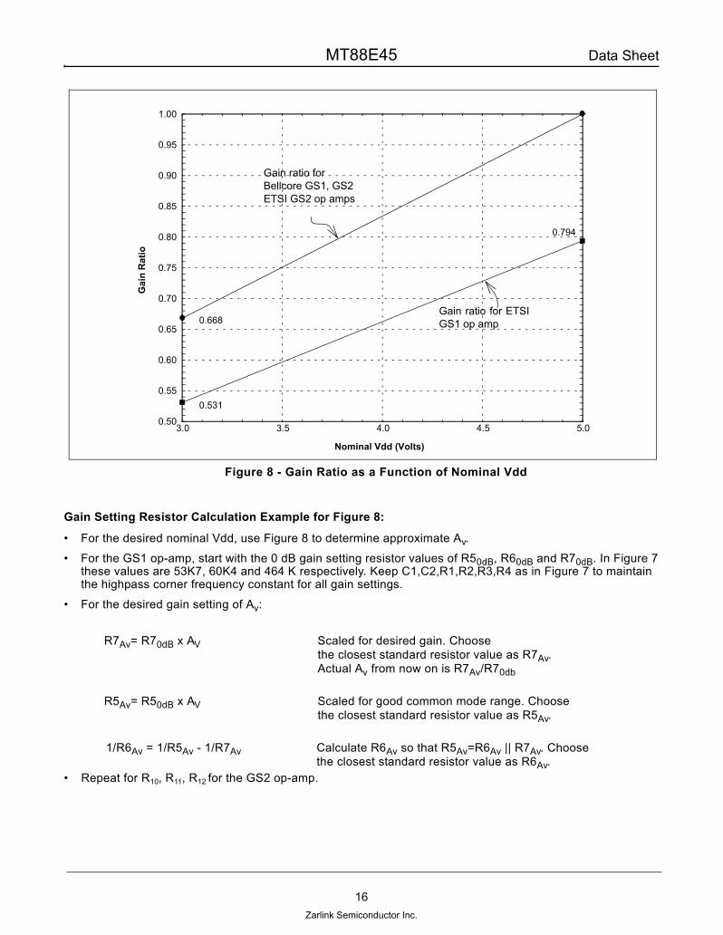
Figure 8 - Gain Ratio as a Function of Nominal Vdd
Gain Setting Resistor Calculation Example for Figure 8:
• For the desired nominal Vdd, use Figure 8 to determine approximate Av.
• For the GS1 op-amp, start with the 0 dB gain setting resistor values of R50dB, R60dB and R70dB. In Figure 7 these values are 53K7, 60K4 and 464 K respectively. Keep C1,C2,R1,R2,R3,R4 as in Figure 7 to maintain the highpass corner frequency constant for all gain settings.
• For the desired gain setting of Av:
R7Av= R70dB x AV Scaled for desired gain. Choose the closest standard resistor value as R7Av.
Actual Av from now on is R7Av/R70db
R5Av= R50dB x AV Scaled for good common mode range. Choose the closest standard resistor value as R5Av.
1/R6Av = 1/R5Av - 1/R7Av Calculate R6Av so that R5Av=R6Av || R7Av. Choosethe closest standard resistor value as R6Av.
• Repeat for R10, R11, R12 for the GS2 op-amp.
3.0 3.5 4.0 4.5 5.0
Nominal Vdd (Volts)
0.50
0.55
0.60
0.65
0.70
0.75
0.80
0.85
0.90
0.95
1.00
Gai
n R
atio
0.668
0.531
0.794
Gain ratio forBellcore GS1, GS2ETSI GS2 op amps
Gain ratio for ETSIGS1 op amp

MT88E45 Data Sheet
17Zarlink Semiconductor Inc.
Example:• For a gain of -3.5 dB, Av=10-3.5/20 = 0.668• R7-3.5dB= 464 K x 0.668 = 309K9, the closest standard resistor value is 309 K.
Av is now 309 K/464 K = 0.666• R5-3.5dB= 53K6 x 0.666 = 35K7, the closest standard resistor value is 35K7.
Therefore R6-3.5dB is calculated to be 40K4, the closest standard resistor value is 40K2.
Figure 9 - Application Circuit: Multiple Interrupt Source
Interrupt Source 1
INT1(Open Drain)
Interrupt Source 2
INT2(CMOS)
MT88E45B
Vdd
Resistor (R1)
Vdd
Resistor (R2)
DR/STD(CMOS)
INT(input)
Microcontroller
Input Port Bit
R1 can be opened and D1 shorted if the microcontroller does not read the INT1 pin.
D1

MT88E45 Data Sheet
18Zarlink Semiconductor Inc.
* Exceeding these values may cause permanent damage. Functional operation under these conditions is not implied.** Under normal operating conditions voltage on any pin except supplies can be minimum VSS-1V to maximum VDD+1V for an input current
limited to less than 200 µΑ
‡ Typical figures are at 25oC and are for design aid only: not guaranteed and not subject to production testing.
Absolute Maximum Ratings* - Voltages are with respect to VSS unless otherwise stated
Parameter Symbol Min. Max. Units
1 Supply voltage with respect to Vss VDD -0.3 6 V
2 Voltage on any pin other than supplies ** VPIN Vss-0.3 VDD+0.3 V
3 Current at any pin other than supplies IPIN 10 mA
4 Storage Temperature TST -65 150 oC
Recommended Operating Conditions - Voltages are with respect to ground (VSS) unless otherwise stated.
Characteristics Sym. Min. Typ.‡ Max. Units
1 Power Supplies VDD 2.7 5.5 V
2 Clock Frequency fOSC 3.579545 MHz
3 Tolerance on Clock Frequency ∆fOSC -0.1 +0.1 %
4 Operating Temperature TOP -40 85 oC
DC Electrical Characteristics†
Characteristics Sym. Min. Typ.‡ Max. Units Test Conditions
1
SUPPLY
Standby Supply Current
IDDQ 0.1 15 µA All inputs are VDD/VSS except for oscillator pins.No analog input.outputs unloaded.CB0/1/2 = 1/0/0
2 Operating Supply CurrentVDD = 5V ±10%VDD = 3V ±10%
IDD
2.81.5
84.5
mAmA
All inputs are VDD/VSS except for oscillator pins.No analog input.outputs unloaded.
3 Power Consumption
PO 44 mW
4
DCLK
Schmitt Input High Threshold
VT+ 0.44*VDD 0.64*VDD V
Schmitt Input Low Threshold
VT- 0.27*VDD 0.47*VDD V
5 Schmitt Hysteresis VHYS 0.2 V6
CB0CB1CB2
CMOS Input High Voltage
VIH 0.7*VDD VDD V
CMOS Input Low Voltage
VIL VSS 0.3*VDD V
7 DCLK DATA
DR/STD CD, ESTST/GT
Output High Source Current
IOH 0.8 mA VOH=0.9*VDD

MT88E45 Data Sheet
19Zarlink Semiconductor Inc.
† DC Electrical Characteristics are over recommended operating conditions, unless otherwise stated.‡ Typical figures are at 25oC and are for design aid only: not guaranteed and not subject to production testing.
† AC Electrical Characteristics are over recommended operating conditions, unless otherwise stated.‡ Typical figures are at 25oC and are for design aid only: not guaranteed and not subject to production testing*Notes:1. Tip/Ring signal level. Input op-amp configured to 0dB gain at Vdd=5V+/-10%, -3.5dB at Vdd=3V+/-10%.2. Tip/Ring signal level. Input op-amp configured to 0dB gain at Vdd=5V+/-10%.3. Both tones have the same amplitude.4. Band limited random noise 300-3400Hz. Measurement valid only when tone is present.5. dBV - Decibels above or below a reference voltage of 1 Vrms. 0 dBV = 1 Vrms. Signal level is per tone.6. dBm - Decibels above or below a reference power of 1 mW into 600 ohms. 0 dBm = 0.7746 Vrms. Signal level is per tone.
8 DCLK DATA
DR/STD CD, ESTST/GT
Output Low Sink Current
IOL 2 mA VOL=0.1*VDD
9 IN1+ IN1- IN2+ IN2-
Input Current Iin1 1 µA Vin=VDD to VSS
DCLK CB0CB1CB2
Iin2 10 µA Vin=VDD to VSS
10 ST/GT Output High-Impedance Current
Ioz1 5 µA Vout =VDD to VSS
11 VREF Output Voltage VREF 0.5VDD -0.1 0.5VDD+0.1 V No Load12 Output Resistance RREF 2 kΩ
13 ST/GT Comparator Threshold Voltage
VTGt 0.5VDD-0.05
0.5VDD+0.05 V
AC Electrical Characteristics† - CAS Detection
Characteristic Sym. Min. Typ.‡ Max. Unit Notes*
1 Lower Tone Frequency fL 2130 Hz
2 Upper Tone Frequency fH 2750 Hz
3 Frequency Deviation: Accept 1.1%range within which
tones are accepted
4 Frequency Deviation: Reject 3.5%range outside of which tones are
rejected
5 Accept Signal Level (per tone)
-40-37.78
-20.22
dBVdBm 1, 5, 6
6 Reject Signal Level (per tone)Vdd=5V +/-10% only
-46-43.78
dBVdBm 2, 5, 6
7 Reject Signal Level (per tone)Vdd=3V+/-10% or 5V+/-10%
-47.22-45
dBVdBm 1, 5, 6
8 Twist: 20 log (V2130Hz/V2750Hz) -7 +7 dB
9 Signal to Noise Ratio SNRCAS 20 dB 3,4
DC Electrical Characteristics† (continued)
Characteristics Sym. Min. Typ.‡ Max. Units Test Conditions
MT88E45 Data Sheet
20Zarlink Semiconductor Inc.
† AC Electrical Characteristics are over recommended operating conditions, unless otherwise stated.‡ Typical figures are nominal values and are for design aid only: not guaranteed and not subject to production testing.*Notes:1. Both mark and space have the same amplitude. 2. Tip/Ring signal level. Input op-amp configured to 0dB gain at Vdd=5V+/-10%, -3.5dB at Vdd=3V+/-10%.3. Band limited random noise (200-3400Hz). Present when FSK signal is present. Note that the BT band is 300-3400Hz, the Bellcore
band is 0-4kHz.4. dBV - Decibels above or below a reference voltage of 1 Vrms. 0 dBV = 1 Vrms.5. dBm - Decibels above or below a reference power of 1 mW into 600 ohms. 0 dBm = 0.7746 Vrms.
† Electrical characteristics are over recommended operating conditions, unless otherwise stated.
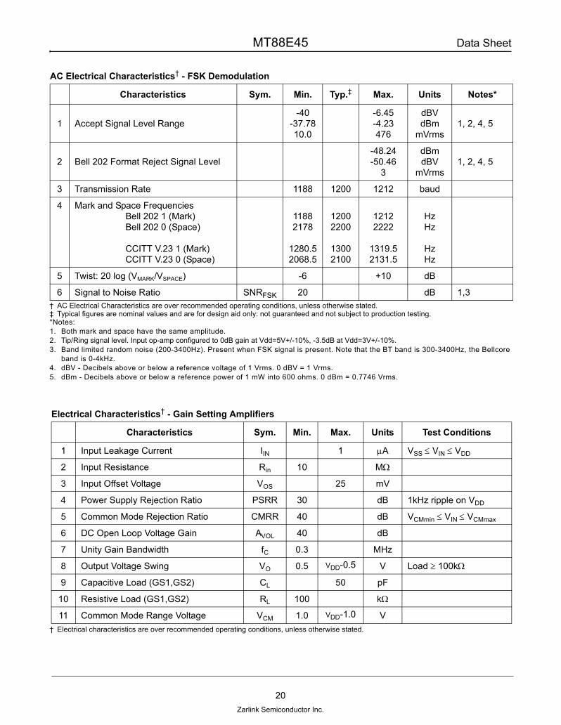
AC Electrical Characteristics† - FSK Demodulation
Characteristics Sym. Min. Typ.‡ Max. Units Notes*
1 Accept Signal Level Range-40
-37.7810.0
-6.45-4.23476
dBVdBm
mVrms1, 2, 4, 5
2 Bell 202 Format Reject Signal Level-48.24-50.46
3
dBmdBV
mVrms1, 2, 4, 5
3 Transmission Rate 1188 1200 1212 baud
4 Mark and Space FrequenciesBell 202 1 (Mark)Bell 202 0 (Space)
CCITT V.23 1 (Mark)CCITT V.23 0 (Space)
11882178
1280.52068.5
12002200
13002100
12122222
1319.52131.5
HzHz
HzHz
5 Twist: 20 log (VMARK/VSPACE) -6 +10 dB
6 Signal to Noise Ratio SNRFSK 20 dB 1,3
Electrical Characteristics† - Gain Setting Amplifiers
Characteristics Sym. Min. Max. Units Test Conditions
1 Input Leakage Current IIN 1 µA VSS ≤ VIN ≤ VDD
2 Input Resistance Rin 10 MΩ
3 Input Offset Voltage VOS 25 mV
4 Power Supply Rejection Ratio PSRR 30 dB 1kHz ripple on VDD
5 Common Mode Rejection Ratio CMRR 40 dB VCMmin ≤ VIN ≤ VCMmax
6 DC Open Loop Voltage Gain AVOL 40 dB
7 Unity Gain Bandwidth fC 0.3 MHz
8 Output Voltage Swing VO 0.5 VDD-0.5 V Load ≥ 100kΩ
9 Capacitive Load (GS1,GS2) CL 50 pF
10 Resistive Load (GS1,GS2) RL 100 kΩ
11 Common Mode Range Voltage VCM 1.0 VDD-1.0 V

MT88E45 Data Sheet
21Zarlink Semiconductor Inc.
† AC Electrical Characteristics are over recommended operating conditions unless otherwise stated.
† AC Electrical Characteristics are over recommended operating conditions unless otherwise stated.
† AC Electrical Characteristics are over recommended operating conditions unless otherwise stated.‡ Typical figures are at 25oC and are for design aid only: not guaranteed and not subject to production testing.*Notes:1. FSK input data at 1200 ±12 baud.2. OSC1 at 3.579545 MHz ±0.1%.3. Function of signal condition.
AC Electrical Characteristics† - CAS Detection Timing
Characteristics Sym. Min. Max. Units Notes
1 Tone present detect time tDP 0.5 10 ms See Figures16 16, 1717
2 Tone absent detect time tDA 0.1 8 ms See Figures16 16, 1717
AC Electrical Characteristics† - Oscillator and Carrier Detect Timing
Characteristics Sym. Min. Max. Units Notes
1OSC2
Power-up time tPU 50 ms
2 Power-down time tPD 10 ms
3
CD
Input FSK to CD low delay tCP 25 ms
4 Input FSK to CD high delay tCA 10 ms
5 Hysteresis 10 ms
AC Electrical Characteristics† - 3-Wire FSK Data Interface Timing (Mode 0)
Characteristics Sym. Min. Typ.‡ Max. Units Notes*
1
DR/STD
Rise time tRR 200 ns into 50 pF Load
2 Fall time tRF 200 ns into 50 pF Load
3 Low time tRL 415 416 417 µs 2
4DATA
Rate 1188 1200 1212 baud 1
5 Input FSK to DATA delay
tIDD 1 5 ms
6
DATADCLK
Rise time tR 200 ns into 50 pF Load
7 Fall time tF 200 ns into 50 pF Load
8 DATA to DCLK delay tDCD 6 416 µs 1, 2, 3
9 DCLK to DATA delay tCDD 6 416 µs 1, 2, 3
10
DCLK
Frequency fDCLK0 1201.6 1202.8 1204 Hz 2
11 High time tCH 415 416 417 µs 2
12 Low time tCL 415 416 417 µs 2
13 DCLKDR/STD
DCLK to DR delay tCRD 415 416 417 µs 2

MT88E45 Data Sheet
22Zarlink Semiconductor Inc.
† AC Electrical Characteristics are over recommended operating conditions unless otherwise stated.
Figure 10 - DATA and DCLK Mode 0 Output Timing
Figure 11 - DR Output Timing
AC Electrical Characteristics† - 3-Wire FSK Data Interface Timing (Mode 1)
Characteristics Sym. Min. Max. Units Notes
1
DCLK
Frequency fDCLK1 1 MHz
2 Duty cycle 30 70 %
3 Rise time tR1 100 ns
4 DCLK DR/STD
DCLK low set up before DR tDDS 500 ns
5 DCLK low hold time after DR tDDH 500 ns
AC Electrical Characteristics - Timing Parameter Measurement Voltage Levels
Characteristics Sym. Level Units Notes
1 CMOS Threshold Voltage VCT 0.5*VDD V
2 Rise/Fall Threshold Voltage High VHM 0.7*VDD V
3 Rise/Fall Threshold Voltage Low VLM 0.3*VDD V
DATA
DCLK
tR
tDCD tCDD
tR
tF
tCL tCH
tF
VHM
VLMVCT
VHM
VLMVCT
tRF tRR
tRL
DRVHM
VLMVCT

MT88E45 Data Sheet
23Zarlink Semiconductor Inc.
Figure 12 - DCLK Mode 1 Input Timing
Figure 13 - 3-Wire FSK Data Interface Timing (Mode 0)
DCLK
tR1
VHM
VLM
TIP/RING(A/B) WIRES
DATA(Output)
DCLK(Output)
DR(Output)
b7 b0 b1 b2 b3 b4 b5 b6 b7 b0 b1 b2 b3 b4 b5 b6 b7 b0 b1 b2 b3 b4 b5
b7 b0 b1 b2 b3 b4 b5 b6 b7 b0 b1 b2 b3 b4 b5 b6 b7 b0 b1 b2 b3b6
stop
start
stop
start
stop
start
stop
start
stop
start
stop
start
tIDD
tCRD
tRL
tCLtCH 1/fDCLK0

MT88E45 Data Sheet
24Zarlink Semiconductor Inc.
Figure 14 - 3-Wire FSK Data Interface Timing (Mode 1)
Figure 15 - Application Timing for Bellcore On-hook Data Transmission Associated with Ringing, e.g., CID
Notes:This on-hook case application is included because a CIDCW (off-hook) CPE must be also capable of receiving on-hook datatransmission (with ringing) from the end office. 1) PWDN and FSKen are internal signals decoded from CB0/1/2. 2) The CPE designer may choose to enable the MT88E45B only after the end of ringing to conserve power in a battery operated CPE.
CD is not activated by ringing. 3) The microcontroller in the CPE powers down the MT88E45B after CD has become inactive.4) The microcontroller times out if CD is not activated.5) This signal represents the mode of the DR/STD pin.
Demodulated Data(Internal Signal)
DCLK (Data Clock)(Schmitt Input)
DR (Data Ready)(Output)
stop start stop0 1 2 3 4 5 6 77
Word N Word N+1
DATA(Output)
5
Word NWord N-1
1/fDCLK1
tRL
>tDDH
The DCLK input must be low before and after DR falling edge.Note 1: DCLK occurs during DR low and returns DR to high.Note 2: DCLK occurs after DR, so DR is low for half a nominal bit time.
>tDDS
43210 6 7 stopstop7 0
Note 1
Note 2
1st Ring 2nd RingCh. seizure Mark Data
A C D E F
..101010.. Data
Note 2 Note 3 Note 2 Note 4
tCAtCP
BTIP/RING
PWDN
OSC2
FSKen
CD
DR
DCLK
DATA
A = 2sec typicalB = 250-500msC = 250msD = 150msE = feature specificMax C+D+E = 2.9 to 3.7secF ≥ 200ms
tPDtPUNote 1
Note 1
Note 5
MT88E45 Data Sheet
25Zarlink Semiconductor Inc.
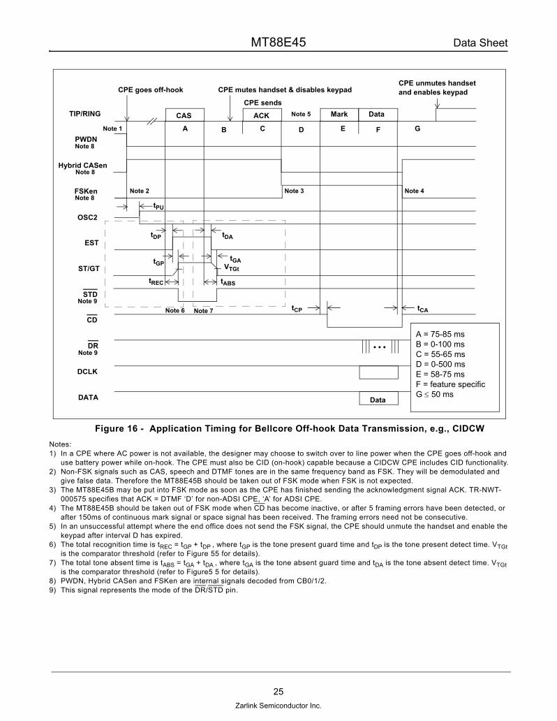
Figure 16 - Application Timing for Bellcore Off-hook Data Transmission, e.g., CIDCWNotes:1) In a CPE where AC power is not available, the designer may choose to switch over to line power when the CPE goes off-hook and
use battery power while on-hook. The CPE must also be CID (on-hook) capable because a CIDCW CPE includes CID functionality.2) Non-FSK signals such as CAS, speech and DTMF tones are in the same frequency band as FSK. They will be demodulated and
give false data. Therefore the MT88E45B should be taken out of FSK mode when FSK is not expected. 3) The MT88E45B may be put into FSK mode as soon as the CPE has finished sending the acknowledgment signal ACK. TR-NWT-
000575 specifies that ACK = DTMF ‘D’ for non-ADSI CPE, ‘A’ for ADSI CPE. 4) The MT88E45B should be taken out of FSK mode when CD has become inactive, or after 5 framing errors have been detected, or
after 150ms of continuous mark signal or space signal has been received. The framing errors need not be consecutive. 5) In an unsuccessful attempt where the end office does not send the FSK signal, the CPE should unmute the handset and enable the
keypad after interval D has expired. 6) The total recognition time is tREC = tGP + tDP , where tGP is the tone present guard time and tDP is the tone present detect time. VTGt
is the comparator threshold (refer to Figure 55 for details).7) The total tone absent time is tABS = tGA + tDA , where tGA is the tone absent guard time and tDA is the tone absent detect time. VTGt
is the comparator threshold (refer to Figure5 5 for details).8) PWDN, Hybrid CASen and FSKen are internal signals decoded from CB0/1/2.9) This signal represents the mode of the DR/STD pin.
CPE goes off-hook
CAS ACK
CPE sends
CPE mutes handset & disables keypad
Mark Data
CPE unmutes handsetand enables keypad
tDP tDA
tGPtGA
tREC tABS
tCP tCA
Data
VTGt
A C E F GB DNote 1
Note 3 Note 4
Note 5TIP/RING
PWDN
FSKen
OSC2
EST
ST/GT
STD
CD
DR
DCLK
DATA
A = 75-85 msB = 0-100 msC = 55-65 msD = 0-500 msE = 58-75 msF = feature specificG ≤ 50 ms
Note 6 Note 7
tPU
Note 8
Note 8
Note 9
Note 2
Note 9
Hybrid CASenNote 8

MT88E45 Data Sheet
26Zarlink Semiconductor Inc.
Figure 17 - Application Timing for BT Caller Display Service (CDS), e.g., CLIPNotes:1) The total recognition time is tREC = tGP + tDP , where tGP is the tone present guard time and tDP is the tone present detect time. VTGt
is the comparator threshold (refer to Figure 55 for details).2) The total tone absent time is tABS = tGA + tDA , where tGA is the tone absent guard time and tDA is the tone absent detect time. VTGt
is the comparator threshold (refer to Figure 55 for details).3) By choosing tGA=15ms, tABS will be 15-25ms so that the current wetting pulse and AC load can be applied right after the STD rising
edge. 4) SIN227 specifies that the AC and DC loads should be removed between 50-150ms after the end of the FSK signal, indicated by CD
returning to high. The MT88E45B may also be powered down at this time.5) The MT88E45B should be taken out of FSK mode when FSK is not expected to prevent the FSK demodulator from reacting to other
in-band signals such as speech, DT-AS/CAS and DTMF tones. 6) PWDN, Tip/Ring CASen, FSKen are internal signals decoded from CB0/1/2.7) This signal represents the mode of the DR/STD pin.
Ch. seizure Mark
..101010.. Data
tDP tDA
tGP tGA
tREC tABS Note 3
tCP tCA
A B C D E F G
Zss (Refer to SIN227)
< 0.5mA (optional)<120µAµ
Note 4
VTGt
Note 5
A/B Wires
PWDN
EST
ST/GT
STD
TE DC load
TE AC load
FSKen
CD
DR
DCLK
DATA
OSC2
Note 1 Note 2
tPU tPD
15±1ms
20±5ms
Note 6
Note 6
Note 7
Note 7
Data
50-150ms
Note 4
Tip/RingCASenNote 6
Ring
Current wetting pulse (see SIN227)
Line Reversal
A ≥ 100 msB = 88-110 msC ≥ 45 ms (up to 5sec)D = 80-262 msE = 45-75 msF ≤ 2.5sec (typ. 500 ms)G > 200 msNote: All valuesobtained from SIN227Issue 1
‘Idle State Tone Alert Signal’DT-AS

MT88E45 Data Sheet
27Zarlink Semiconductor Inc.
Figure 18 - Application Timing for UK’s CCA Caller Display Service (CDS), e.g., CLIPNotes:1) From TW/P&E/312. Start time: The CPE should enter the signalling state by applying the DC and AC terminations within this time
after the end of the ring burst. 2) End time: The CPE should leave the signalling state by removing the DC and AC terminations within this time after the end of Data,
indicated by CD returning to high. The MT88E45B should also be taken out of FSK mode at this time to prevent the FSK demodulator from reacting to other in-band signals such as speech, and DTMF tones.
3) PWDN and FSKen are internal signals decoded from CB0/1/2. 4) This signal represents the mode of the DR/STD pin.
Ch. seizure Mark Data
..101010.. Data
Note 1
tCP tCA
A B C D E FA/B Wires
PWDN
TE DC load
TE AC load
FSKen
CD
DR
DCLK
DATA
OSC2
Note 2
A = 200-450 msB ≥ 500 msC = 80-262 msD = 45-262 msE ≤ 2.5s (typ. 500 ms)F >200 msNote: Parameter Ffrom "CCA ExceptionsDocument Issue 3"
tPU tPD
Note 3
Note 3
Note 4
Ring Burst
First CompleteRing Cycle
250-400ms50-150ms
Line Reversal (Optionally sent)

www.zarlink.com
Information relating to products and services furnished herein by Zarlink Semiconductor Inc. or its subsidiaries (collectively “Zarlink”) is believed to be reliable.However, Zarlink assumes no liability for errors that may appear in this publication, or for liability otherwise arising from the application or use of any suchinformation, product or service or for any infringement of patents or other intellectual property rights owned by third parties which may result from such application oruse. Neither the supply of such information or purchase of product or service conveys any license, either express or implied, under patents or other intellectualproperty rights owned by Zarlink or licensed from third parties by Zarlink, whatsoever. Purchasers of products are also hereby notified that the use of product incertain ways or in combination with Zarlink, or non-Zarlink furnished goods or services may infringe patents or other intellectual property rights owned by Zarlink.
This publication is issued to provide information only and (unless agreed by Zarlink in writing) may not be used, applied or reproduced for any purpose nor form partof any order or contract nor to be regarded as a representation relating to the products or services concerned. The products, their specifications, services and otherinformation appearing in this publication are subject to change by Zarlink without notice. No warranty or guarantee express or implied is made regarding thecapability, performance or suitability of any product or service. Information concerning possible methods of use is provided as a guide only and does not constituteany guarantee that such methods of use will be satisfactory in a specific piece of equipment. It is the user’s responsibility to fully determine the performance andsuitability of any equipment using such information and to ensure that any publication or data used is up to date and has not been superseded. Manufacturing doesnot necessarily include testing of all functions or parameters. These products are not suitable for use in any medical products whose failure to perform may result insignificant injury or death to the user. All products and materials are sold and services provided subject to Zarlink’s conditions of sale which are available on request.
Purchase of Zarlink’s I2C components conveys a licence under the Philips I2C Patent rights to use these components in and I2C System, provided that the systemconforms to the I2C Standard Specification as defined by Philips.
Zarlink, ZL, the Zarlink Semiconductor logo and the Legerity logo and combinations thereof, VoiceEdge, VoicePort, SLAC, ISLIC, ISLAC and VoicePath aretrademarks of Zarlink Semiconductor Inc.
TECHNICAL DOCUMENTATION - NOT FOR RESALE
For more information about all Zarlink productsvisit our Web Site at