William Stallings Computer Organization and...
38
William Stallings Computer Organization and Architecture Chapter 16 16 - Rev. 3.2 (2009-10) by Enrico Nardelli 1 Control Unit Operations
Transcript of William Stallings Computer Organization and...
William Stallings
Computer Organization
and Architecture
Chapter 16
16 -Rev. 3.2 (2009-10) by Enrico Nardelli 1
Chapter 16
Control Unit Operations
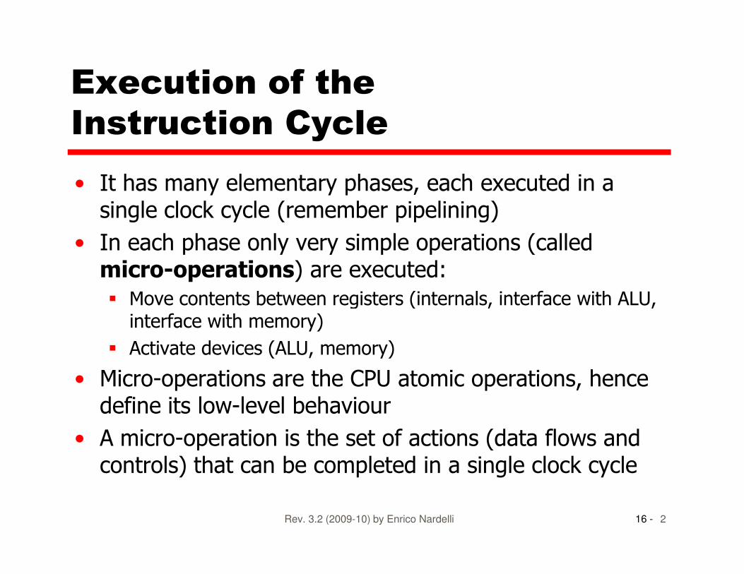
Execution of the
Instruction Cycle
• It has many elementary phases, each executed in a single clock cycle (remember pipelining)
• In each phase only very simple operations (called micro-operations) are executed:
Move contents between registers (internals, interface with ALU,
16 -Rev. 3.2 (2009-10) by Enrico Nardelli 2
� Move contents between registers (internals, interface with ALU, interface with memory)
� Activate devices (ALU, memory)
• Micro-operations are the CPU atomic operations, hence define its low-level behaviour
• A micro-operation is the set of actions (data flows and controls) that can be completed in a single clock cycle
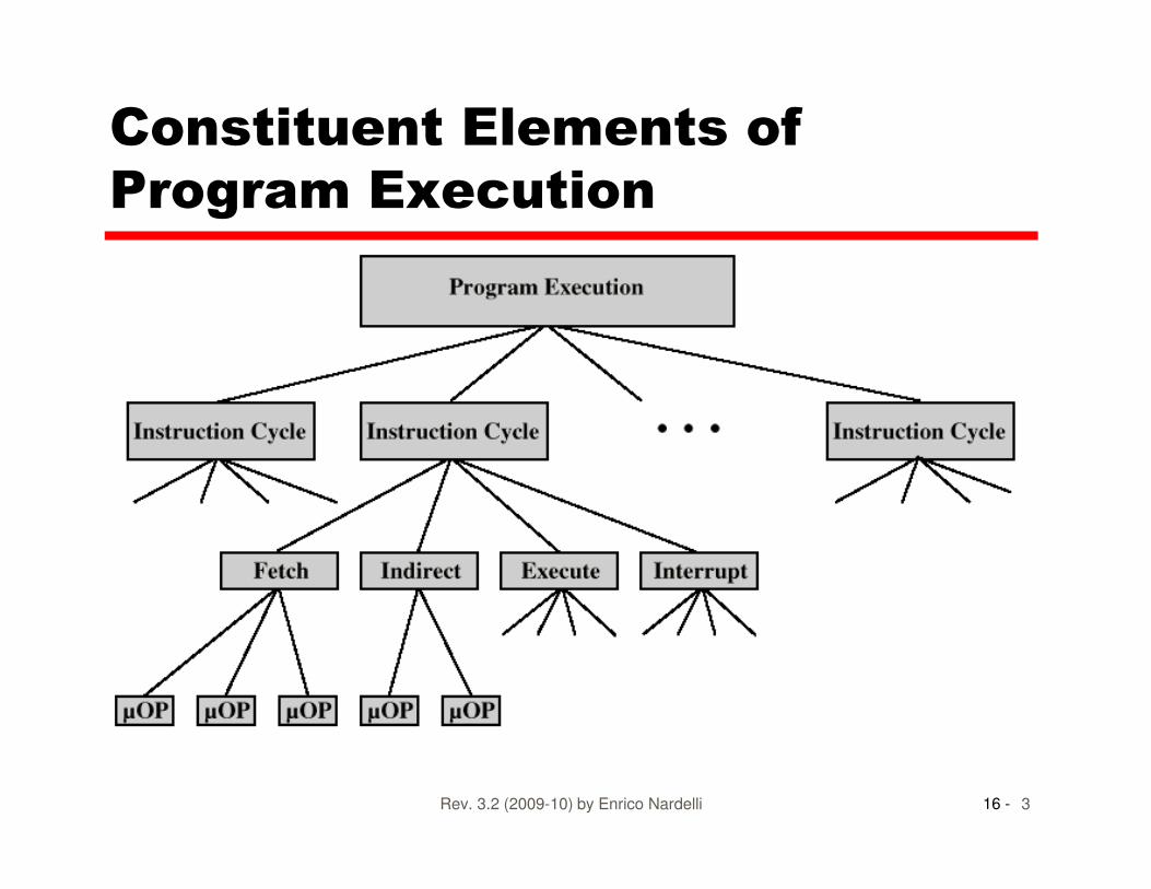
Constituent Elements of
Program Execution
16 -Rev. 3.2 (2009-10) by Enrico Nardelli 3
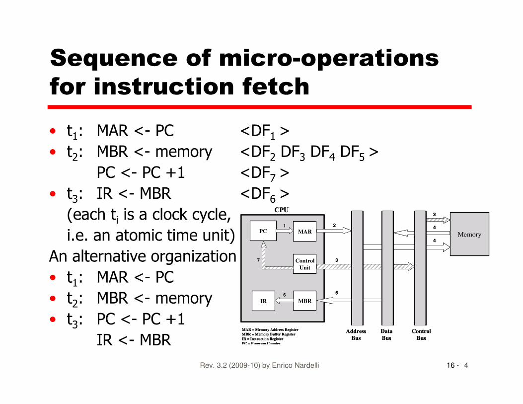
Sequence of micro-operations
for instruction fetch
• t1: MAR <- PC <DF1 >
• t2: MBR <- memory <DF2 DF3 DF4 DF5 >
PC <- PC +1 <DF7 >
• t3: IR <- MBR <DF6 >
16 -Rev. 3.2 (2009-10) by Enrico Nardelli 4
3 6
(each ti is a clock cycle,
i.e. an atomic time unit)
An alternative organization
• t1: MAR <- PC
• t2: MBR <- memory
• t3: PC <- PC +1
IR <- MBR
IR MBR
Control
Unit
MAR
Data
Bus
Address
Bus
Control
Bus
Memory
CPU
MAR = Memory Address Register
MBR = Memory Buffer Register
IR = Instruction Register
PC = Program Counter
PC2
3
3
4
4
5
1
6
7
IR MBR
Control
Unit
MAR
Data
Bus
Address
Bus
Control
Bus
Memory
CPU
MAR = Memory Address Register
MBR = Memory Buffer Register
IR = Instruction Register
PC = Program Counter
PC2
3
3
4
4
5
1
6
7
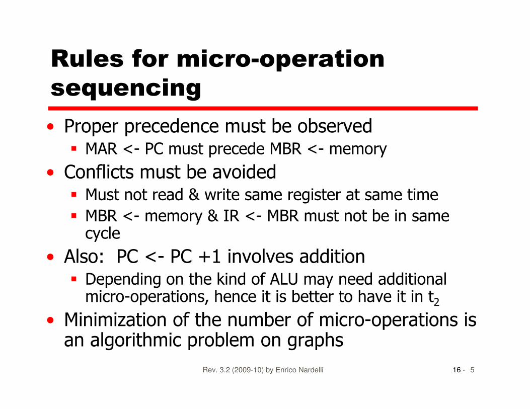
Rules for micro-operation
sequencing
• Proper precedence must be observed� MAR <- PC must precede MBR <- memory
• Conflicts must be avoided� Must not read & write same register at same time
16 -Rev. 3.2 (2009-10) by Enrico Nardelli 5
� MBR <- memory & IR <- MBR must not be in same cycle
• Also: PC <- PC +1 involves addition� Depending on the kind of ALU may need additional micro-operations, hence it is better to have it in t2
• Minimization of the number of micro-operations is an algorithmic problem on graphs
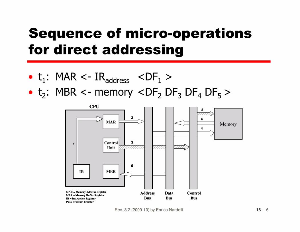
Sequence of micro-operations
for direct addressing
• t1: MAR <- IRaddress <DF1 >
• t2: MBR <- memory <DF2 DF3 DF4 DF5 >CPU
2
3CPU
2
3
16 -Rev. 3.2 (2009-10) by Enrico Nardelli 6
IR MBR
Control
Unit
MAR
Data
Bus
Address
Bus
Control
Bus
Memory
MAR = Memory Address Register
MBR = Memory Buffer Register
IR = Instruction Register
PC = Program Counter
2
3
4
4
5
1
IR MBR
Control
Unit
MAR
Data
Bus
Address
Bus
Control
Bus
Memory
MAR = Memory Address Register
MBR = Memory Buffer Register
IR = Instruction Register
PC = Program Counter
2
3
4
4
5
1
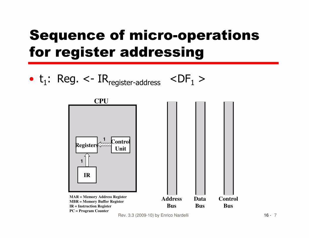
• t1: Reg. <- IRregister-address <DF1 >
Sequence of micro-operations
for register addressing
CPU
16 -Rev. 3.3 (2009-10) by Enrico Nardelli 7
IR
Control
UnitRegisters
Data
Bus
Address
Bus
Control
Bus
MAR = Memory Address Register
MBR = Memory Buffer Register
IR = Instruction Register
PC = Program Counter
1
1
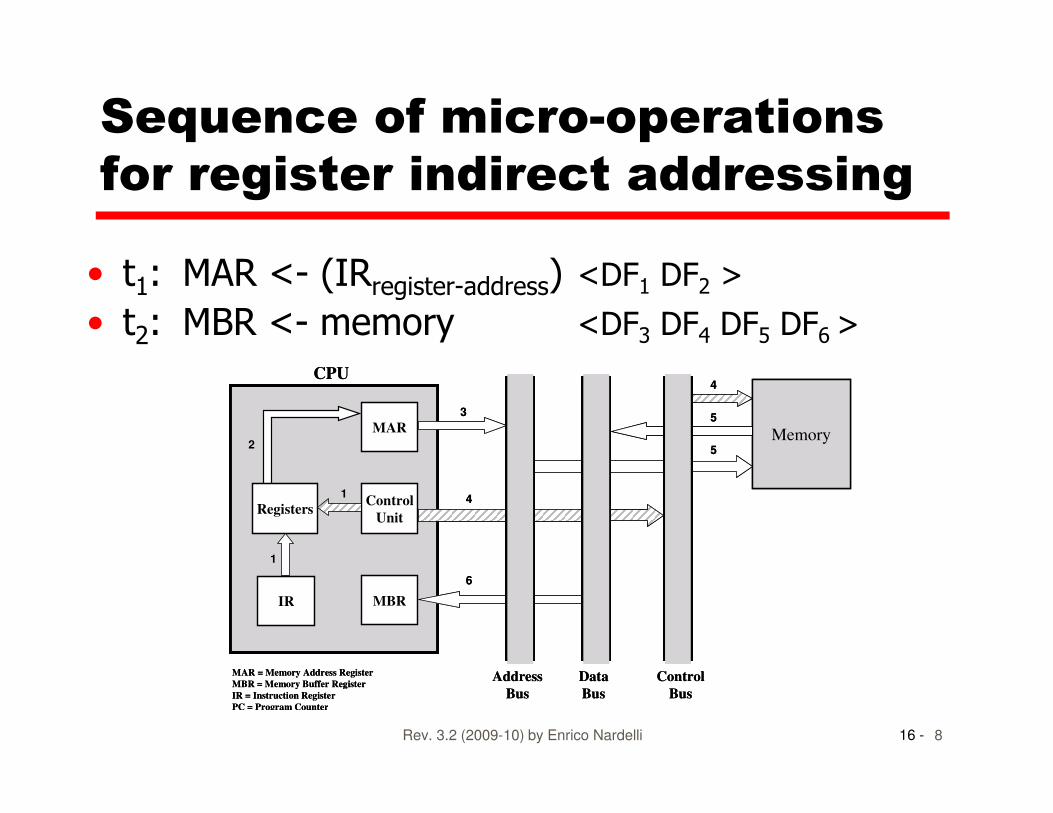
Sequence of micro-operations
for register indirect addressing
• t1: MAR <- (IRregister-address) <DF1 DF2 >
• t2: MBR <- memory <DF3 DF4 DF5 DF6 >
CPU
3
4CPU
3
4
16 -Rev. 3.2 (2009-10) by Enrico Nardelli 8
IR MBR
Control
Unit
MAR
Data
Bus
Address
Bus
Control
Bus
Memory
MAR = Memory Address Register
MBR = Memory Buffer Register
IR = Instruction Register
PC = Program Counter
Registers
3
4
5
5
6
1
1
2
IR MBR
Control
Unit
MAR
Data
Bus
Address
Bus
Control
Bus
Memory
MAR = Memory Address Register
MBR = Memory Buffer Register
IR = Instruction Register
PC = Program Counter
Registers
3
4
5
5
6
1
1
2
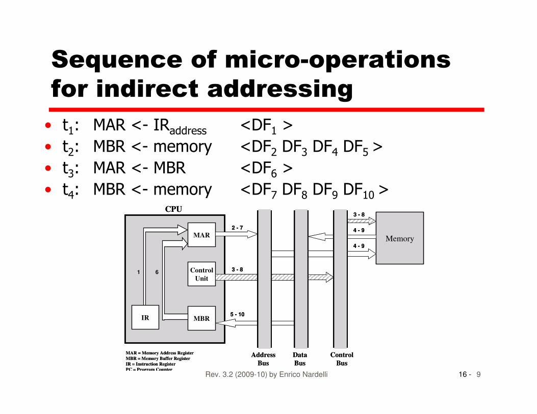
Sequence of micro-operations
for indirect addressing
• t1: MAR <- IRaddress <DF1 >
• t2: MBR <- memory <DF2 DF3 DF4 DF5 >
• t3: MAR <- MBR <DF6 >
• t4: MBR <- memory <DF7 DF8 DF9 DF10 >CPUCPU
16 -Rev. 3.2 (2009-10) by Enrico Nardelli 9
MBR
Control
Unit
MAR
Data
Bus
Address
Bus
Control
Bus
Memory
CPU
MAR = Memory Address Register
MBR = Memory Buffer Register
IR = Instruction Register
PC = Program Counter
2 - 7
3 - 8
3 - 8
4 - 9
4 - 9
5 - 10
1
IR
6
MBR
Control
Unit
MAR
Data
Bus
Address
Bus
Control
Bus
Memory
CPU
MAR = Memory Address Register
MBR = Memory Buffer Register
IR = Instruction Register
PC = Program Counter
2 - 7
3 - 8
3 - 8
4 - 9
4 - 9
5 - 10
1
IR
6
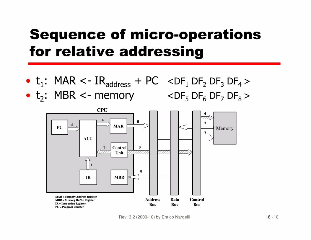
Sequence of micro-operations
for relative addressing
• t1: MAR <- IRaddress + PC <DF1 DF2 DF3 DF4 >
• t2: MBR <- memory <DF5 DF6 DF7 DF8 >
CPU
5
6
4
CPU
5
6
4
16 -Rev. 3.2 (2009-10) by Enrico Nardelli 10
IR MBR
Control
Unit
MAR
Data
Bus
Address
Bus
Control
Bus
Memory
MAR = Memory Address Register
MBR = Memory Buffer Register
IR = Instruction Register
PC = Program Counter
ALU = Arithmetic Logic Unit
ALU
PC
5
6
7
7
8
1
2
3
4
IR MBR
Control
Unit
MAR
Data
Bus
Address
Bus
Control
Bus
Memory
MAR = Memory Address Register
MBR = Memory Buffer Register
IR = Instruction Register
PC = Program Counter
ALU = Arithmetic Logic Unit
ALU
PC
5
6
7
7
8
1
2
3
4
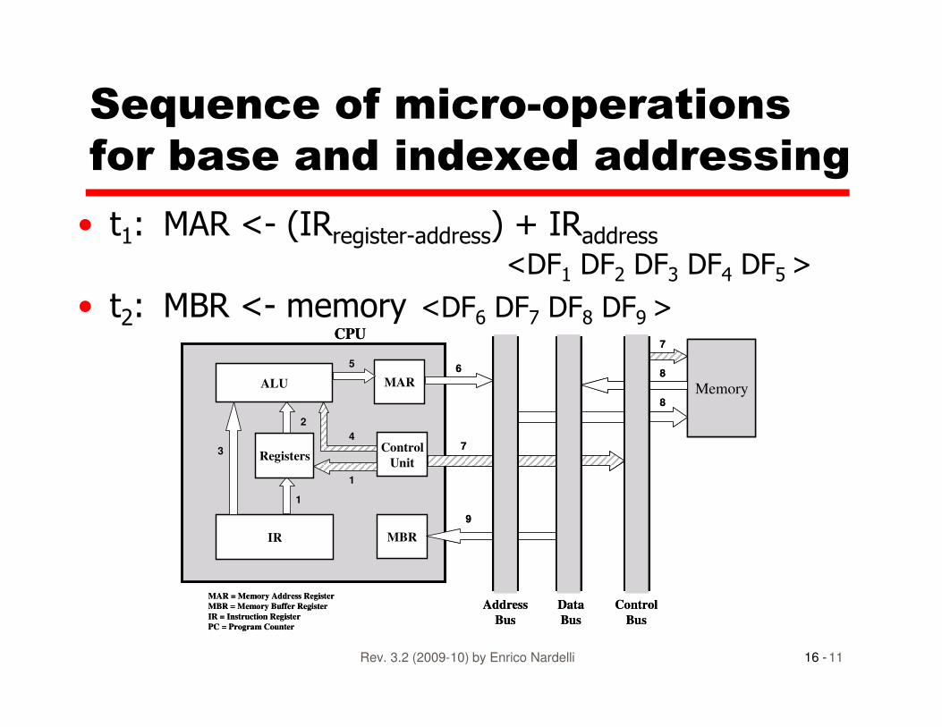
Sequence of micro-operations
for base and indexed addressing
• t1: MAR <- (IRregister-address) + IRaddress<DF1 DF2 DF3 DF4 DF5 >
• t2: MBR <- memory <DF6 DF7 DF8 DF9 >CPU
56
7CPU
56
7
16 -Rev. 3.2 (2009-10) by Enrico Nardelli 11
IR MBR
Control
Unit
MAR
Data
Bus
Address
Bus
Control
Bus
Memory
MAR = Memory Address Register
MBR = Memory Buffer Register
IR = Instruction Register
PC = Program Counter
ALU = Arithmetic Logic Unit
Registers
1
1
2
3
5
ALU
4
6
7
8
8
9
IR MBR
Control
Unit
MAR
Data
Bus
Address
Bus
Control
Bus
Memory
MAR = Memory Address Register
MBR = Memory Buffer Register
IR = Instruction Register
PC = Program Counter
ALU = Arithmetic Logic Unit
Registers
1
1
2
3
5
ALU
4
6
7
8
8
9
Sequence of micro-operations for
combination of displacement and
indirect addressing
• Try them yourself !
16 -Rev. 3.2 (2009-10) by Enrico Nardelli 12
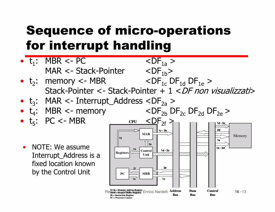
Sequence of micro-operations
for interrupt handling• t1: MBR <- PC <DF1a >
MAR <- Stack-Pointer <DF1b>• t2: memory <- MBR <DF1c DF1d DF1e >
Stack-Pointer <- Stack-Pointer + 1 <DF non visualizzati>• t3: MAR <- Interrupt_Address <DF2a >• t : MBR <- memory <DF DF DF DF >
16 -Rev. 3.2 (2009-10) by Enrico Nardelli 13
3 2a
• t4: MBR <- memory <DF2b DF2c DF2d DF2e >• t5: PC <- MBR <DF2f >
MAR
Data
Bus
Address
Bus
Control
Bus
Memory
CPU
MAR = Memory Address Register
MBR = Memory Buffer Register
IR = Instruction Register
PC = Program Counter
Registers
PC
Control
Unit
MBR
1b
1a
1b
1c - 2b
1c
1d - 2c
1d - 2c
1e
1e - 2d
2a
2d
2e2f
MAR
Data
Bus
Address
Bus
Control
Bus
Memory
CPU
MAR = Memory Address Register
MBR = Memory Buffer Register
IR = Instruction Register
PC = Program Counter
Registers
PC
Control
Unit
MBR
1b
1a
1b
1c - 2b
1c
1d - 2c
1d - 2c
1e
1e - 2d
2a
2d
2e2f
• NOTE: We assume Interrupt_Address is a fixed location known by the Control Unit
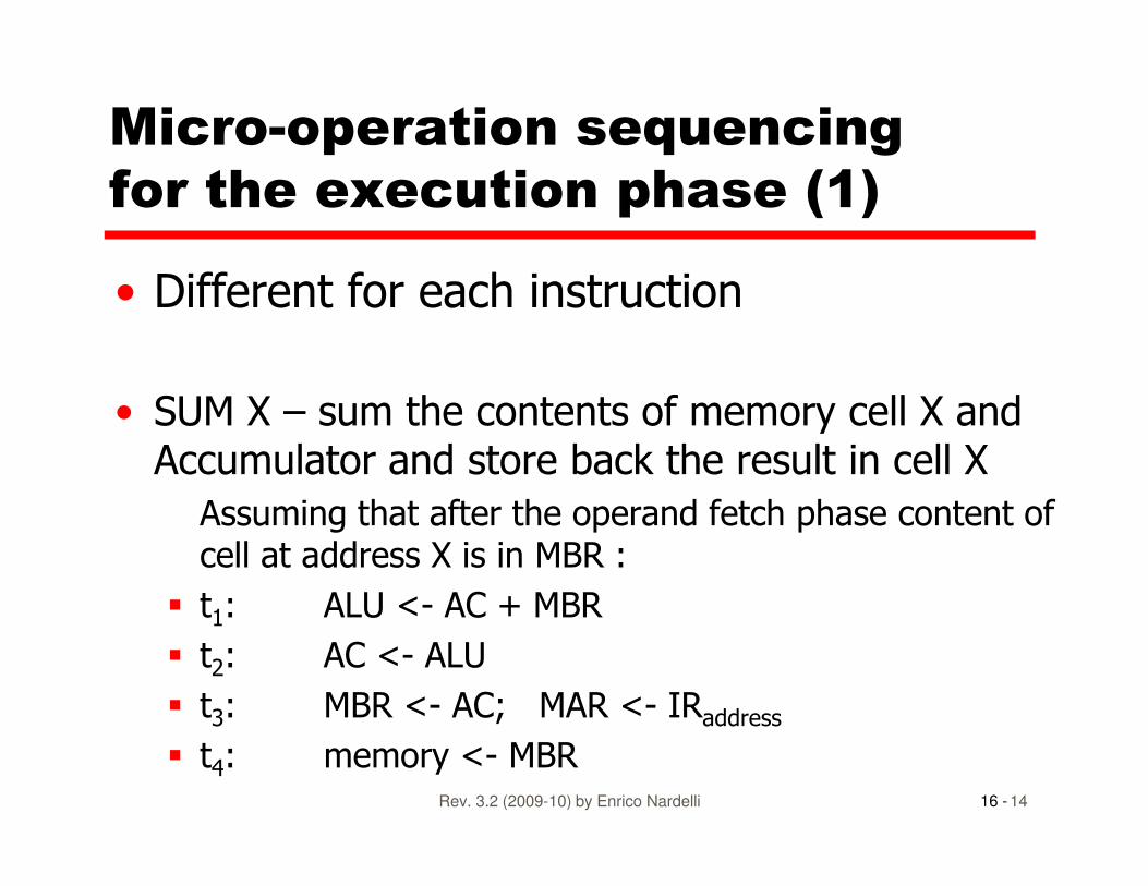
Micro-operation sequencing
for the execution phase (1)
• Different for each instruction
• SUM X – sum the contents of memory cell X and Accumulator and store back the result in cell X
16 -Rev. 3.2 (2009-10) by Enrico Nardelli 14
Accumulator and store back the result in cell X
Assuming that after the operand fetch phase content of cell at address X is in MBR :
� t1: ALU <- AC + MBR
� t2: AC <- ALU
� t3: MBR <- AC; MAR <- IRaddress� t4: memory <- MBR
Micro-operation sequencing
for the execution phase (2)
• ISZ X - increment memory cell X and if it’s zero skip the next instruction
Assuming that content of cell at address X is in MBR after the operand fetch phase:
16 -Rev. 3.2 (2009-10) by Enrico Nardelli 15
the operand fetch phase:
� t1: ALU <- MBR + 1
� t2: MBR <- ALU
� t3: memory <- MBR
IF MBR == 0 THEN PC <- PC + 1
• Note:
� IF-THEN is a single micro-operation
Micro-operation sequencing
for the execution phase (3)
• CALL X - Save in stack the return address and jump to address X
� t1: MBR <- PC
MAR <- SP
16 -Rev. 3.2 (2009-10) by Enrico Nardelli 16
MAR <- SP
� t2: memory <- MBR
ALU <- SP + 1
PC <- IRaddress� t3: SP <- ALU
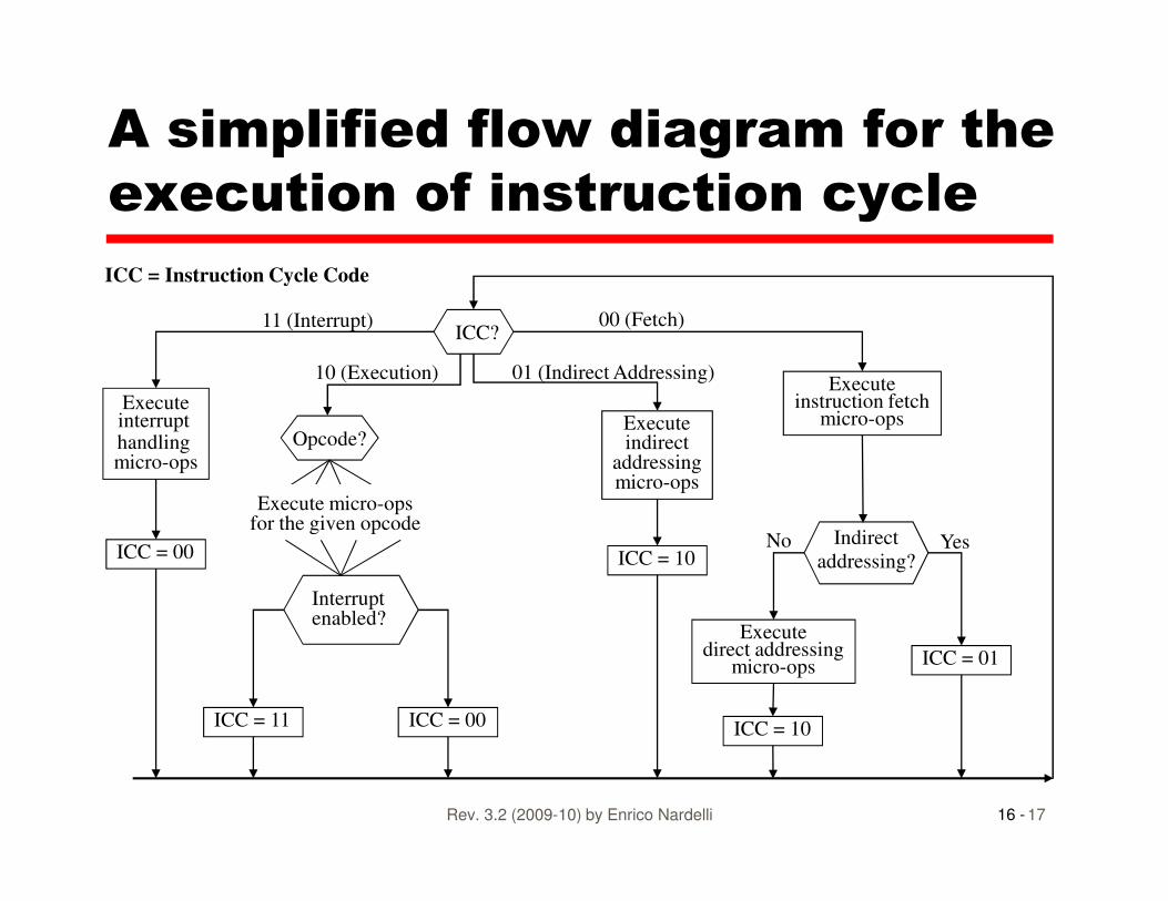
A simplified flow diagram for the
execution of instruction cycle
Executeinterrupt handling micro-ops
Opcode?
ICC?
Executeinstruction fetch
micro-opsExecuteindirect
addressing
11 (Interrupt) 00 (Fetch)
01 (Indirect Addressing)10 (Execution)
ICC = Instruction Cycle Code
16 -Rev. 3.2 (2009-10) by Enrico Nardelli 17
Interrupt enabled?
handling micro-ops
Indirect
addressing?
indirectaddressingmicro-ops
ICC = 10
ICC = 01
ICC = 10ICC = 00ICC = 11
ICC = 00
Execute micro-opsfor the given opcode
YesNo
Executedirect addressing
micro-ops
Functions of Control Unit
• Sequencing
� Causing the CPU to step through a series of micro-operations
• Execution
16 -Rev. 3.2 (2009-10) by Enrico Nardelli 18
• Execution
� Causing the execution of each micro-op
• ALL THESE ACTIONS are performed by means of Control Signals
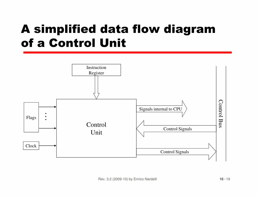
A simplified data flow diagram
of a Control Unit
Instruction
Register
16 -Rev. 3.2 (2009-10) by Enrico Nardelli 19
Control
Unit
Contro
l Bus
Control Signals
Control Signals
Signals internal to CPU
Clock
Flags
…
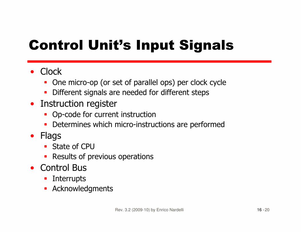
Control Unit’s Input Signals
• Clock� One micro-op (or set of parallel ops) per clock cycle
� Different signals are needed for different steps
• Instruction register� Op-code for current instruction
16 -Rev. 3.2 (2009-10) by Enrico Nardelli 20
� Op-code for current instruction
� Determines which micro-instructions are performed
• Flags� State of CPU
� Results of previous operations
• Control Bus� Interrupts
� Acknowledgments
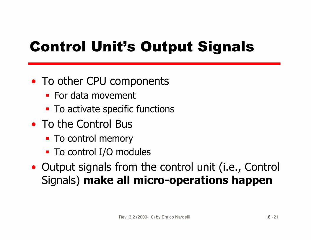
Control Unit’s Output Signals
• To other CPU components
� For data movement
� To activate specific functions
• To the Control Bus
16 -Rev. 3.2 (2009-10) by Enrico Nardelli 21
• To the Control Bus
� To control memory
� To control I/O modules
• Output signals from the control unit (i.e., Control Signals) make all micro-operations happen
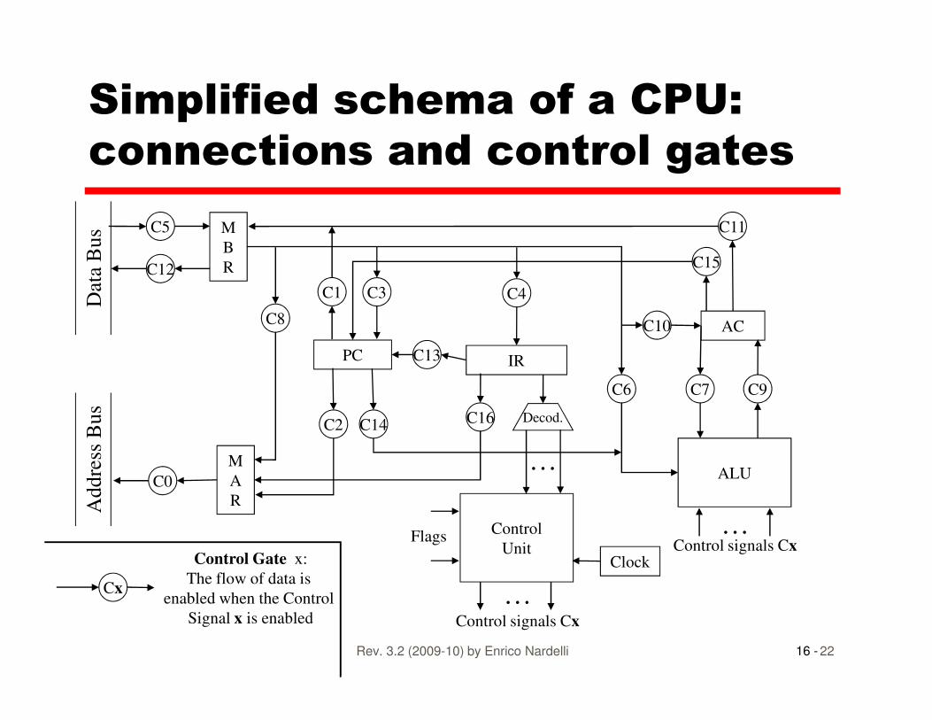
Simplified schema of a CPU:
connections and control gates
M
B
R
C5
C12
PC IR
AC
C11
C10
C4
C13
C3C1
C8
C15
Dat
a B
us
16 -Rev. 3.2 (2009-10) by Enrico Nardelli 22
M
A
R
C0
PC IR
Control
Unit
ALU
C9C7C6
C13
C2
Clock
…Control signals Cx
Flags
Cx
Control Gate x:
The flow of data is
enabled when the Control
Signal x is enabled
…Control signals Cx
C14 C16 Decod.
…
Addre
ss B
us
Example of Control Signal
Sequence – Instruction Fetch (1)
• t1: MAR <- PC
� Control unit (CU) activates signal C2 to open gate from PC to MAR
• t : MBR <- memory
16 -Rev. 3.2 (2009-10) by Enrico Nardelli 23
• t2-1: MBR <- memory
� CU activates C0 to open gate from MAR to address bus
� CU activates the memory read control signal (CR -not shown) to the memory
� CU activates C5 to open gate from data bus to MBR
Example of Control Signal
Sequence – Instruction Fetch (2)
• t2-2: PC <- PC +1� In the considered CPU’s internal schema, ALU’s output is not directly connected to PC but only to AC. Therefore this micro-operation has to be split in two subsequent time units.
16 -Rev. 3.2 (2009-10) by Enrico Nardelli 24
subsequent time units.
� What would happen if we had ALU’s output directly connected to PC?
• t3: IR <- MBR� CU activates C4 to open gate from MBR to IR
Example of Control Signal
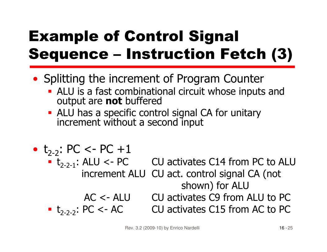
Sequence – Instruction Fetch (3)
• Splitting the increment of Program Counter� ALU is a fast combinational circuit whose inputs and output are not buffered
� ALU has a specific control signal CA for unitary increment without a second input
16 -Rev. 3.2 (2009-10) by Enrico Nardelli 25
increment without a second input
• t2-2: PC <- PC +1� t2-2-1: ALU <- PC CU activates C14 from PC to ALU
increment ALU CU act. control signal CA (notshown) for ALU
AC <- ALU CU activates C9 from ALU to PC� t2-2-2: PC <- AC CU activates C15 from AC to PC
Example of Control Signal
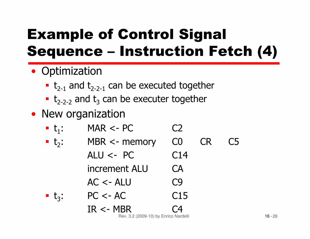
Sequence – Instruction Fetch (4)
• Optimization
� t2-1 and t2-2-1 can be executed together
� t2-2-2 and t3 can be executer together
• New organization
16 -Rev. 3.2 (2009-10) by Enrico Nardelli 26
• New organization
� t1: MAR <- PC C2
� t2: MBR <- memory C0 CR C5
ALU <- PC C14
increment ALU CA
AC <- ALU C9
� t3: PC <- AC C15
IR <- MBR C4
Example of Control Signal
Sequence - Direct Addressing
• Direct addressing is executed right after instruction fetch in our simplified flow diagram for the execution of an instruction cycle. Hence:
• t4: MAR <- IRaddress
16 -Rev. 3.2 (2009-10) by Enrico Nardelli 27
• t4: MAR <- IRaddress� CU activates C16 to open gate from IR to MAR
• t5: MBR <- memory
� CU act. C0 to open gate from MAR to address bus
� CU act. the memory read control signal CR
� CU act. C5 to open gate from data bus to MBR
Example of Control Signal
Sequence - Indirect Addressing
• t1: MAR <- IRaddress� CU activates C16 to open gate from IR to MAR
• t2: MBR <- memory
� CU act. C0 to open gate from MAR to address bus
16 -Rev. 3.2 (2009-10) by Enrico Nardelli 28
� CU act. C0 to open gate from MAR to address bus
� CU act. the memory read control signal CR
� CU act. C5 to open gate from data bus to MBR
• t3: MAR <- MBR
� CU activates C8 to open gate from MBR to MAR
• t4: MBR <- memory
� CU activates C0, CR and C5 as above
Example of Control Signal
Sequence – Execution: SUM
• t1: ALU <- AC + MBR� CU activates C6 to open gate from MBR to ALU� CU activates C7 to open gate from AC to ALU� CU activates for the ALU the sum control signal CS
• t2: AC <- ALU� CU activates C9 to open gate from ALU to AC
• t : MBR <- AC; MAR <- IR
16 -Rev. 3.2 (2009-10) by Enrico Nardelli 29
• t2: MBR <- AC; MAR <- IRaddress� CU activates C11 to open gate from AC to MBR� CU activates C16 to open gate from IR to MAR
• t2: memory <- MBR� CU activates C0 to open gate from MAR to address bus� CU activates C12 to open gate from MBR to data bus� CU activates the memory write control signal CW
• NOTE: Now ALU’s output needs to be “buffered”: this means that its output lines are not directly coming from the internal combinational circuits but from a registry (buffer) that receives combinational circuits outputs and store them for a subsequent reading
Limitations
• The simplified internal schema of a CPU does not show registers, hence we cannot show� Register addressing
� Register indirect addressing
� Base addressing
16 -Rev. 3.2 (2009-10) by Enrico Nardelli 30
� Base addressing
� Indexed addressing
� Combination of displacement and indirect addressing
� Try adding to the simplified schema one or more of the above addressing modalities and derive the required micro-operations!
Internal Organization of CPU
• Usually a single internal bus
� less complex then having direct data paths between registers and ALU
• Control gates control movement of data onto and off the internal bus
16 -Rev. 3.2 (2009-10) by Enrico Nardelli 31
off the internal bus
• Control signals control also data transfer to and from external systems bus
• Temporary registers (i.e., buffers) in input to ALU are now needed for proper operation of ALU
• After Appendix B try yourself deriving the control signal sequences for a single internal bus CPU!
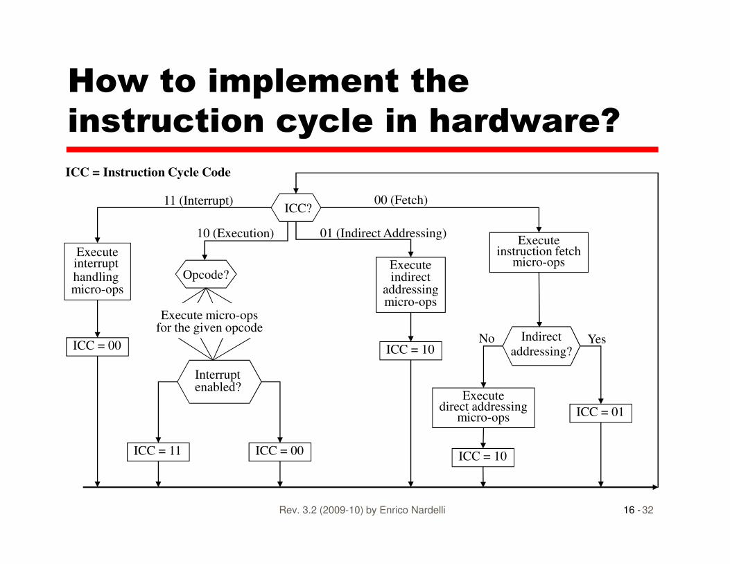
How to implement the
instruction cycle in hardware?
Executeinterrupt handling micro-ops
Opcode?
ICC?
Executeinstruction fetch
micro-opsExecuteindirect
addressing
11 (Interrupt) 00 (Fetch)
01 (Indirect Addressing)10 (Execution)
ICC = Instruction Cycle Code
16 -Rev. 3.2 (2009-10) by Enrico Nardelli 32
Interrupt enabled?
handling micro-ops
Indirect
addressing?
indirectaddressingmicro-ops
ICC = 10
ICC = 01
ICC = 10ICC = 00ICC = 11
ICC = 00
Execute micro-opsfor the given opcode
YesNo
Executedirect addressing
micro-ops
Hardwired Implementation (1)
• Consider the control unit as a combinational circuit� Outputs of the circuit are the control signals
� Inputs of the circuit are:• ICC register bits (note that ICC is not visualized in the CPU’s simplified internal schema)
16 -Rev. 3.2 (2009-10) by Enrico Nardelli 33
simplified internal schema)
• Status flags, including interrupt-enable/disable (T)
• Direct/indirect address bit (D)
• Decoded opcodes (OCn)
• Clocks (tn)
� For each configuration of inputs produce a proper output
� That is, the activation of a given control signal Cn has to happen when (condition A is true) OR (condition B is true) OR …
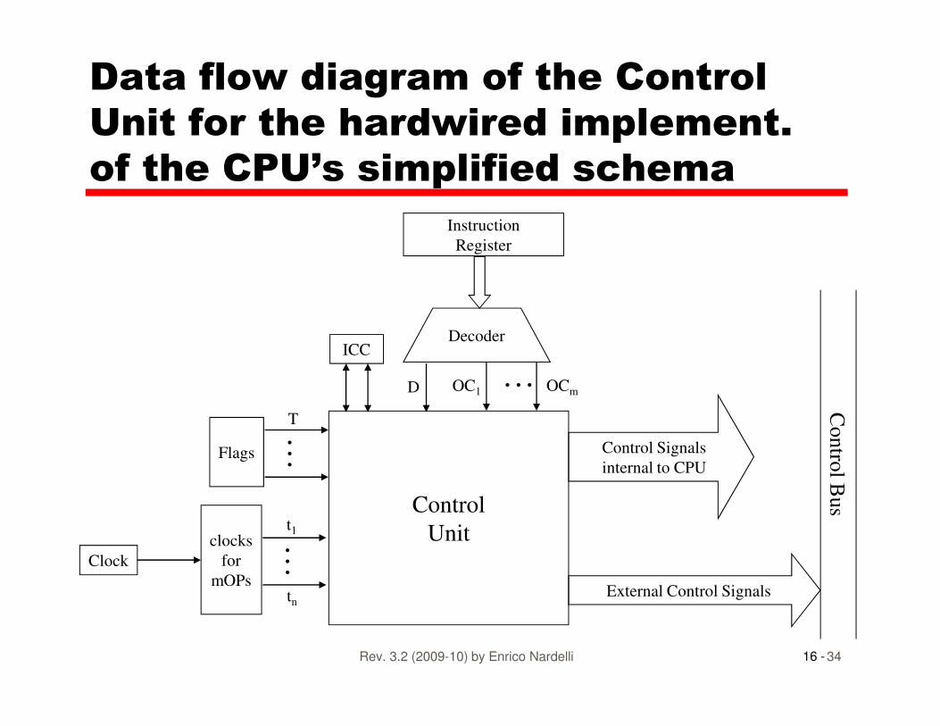
Data flow diagram of the Control
Unit for the hardwired implement.
of the CPU’s simplified schema
Instruction
Register
Decoder
…ICC
16 -Rev. 3.2 (2009-10) by Enrico Nardelli 34
Control
Unit
Contro
l Bus
External Control Signals
Control Signals
internal to CPU
Clock
Flags
…
clocks
for
mOPs
…t1
tn
…OC1 OCmD
T
Hardwired Implementation (2)
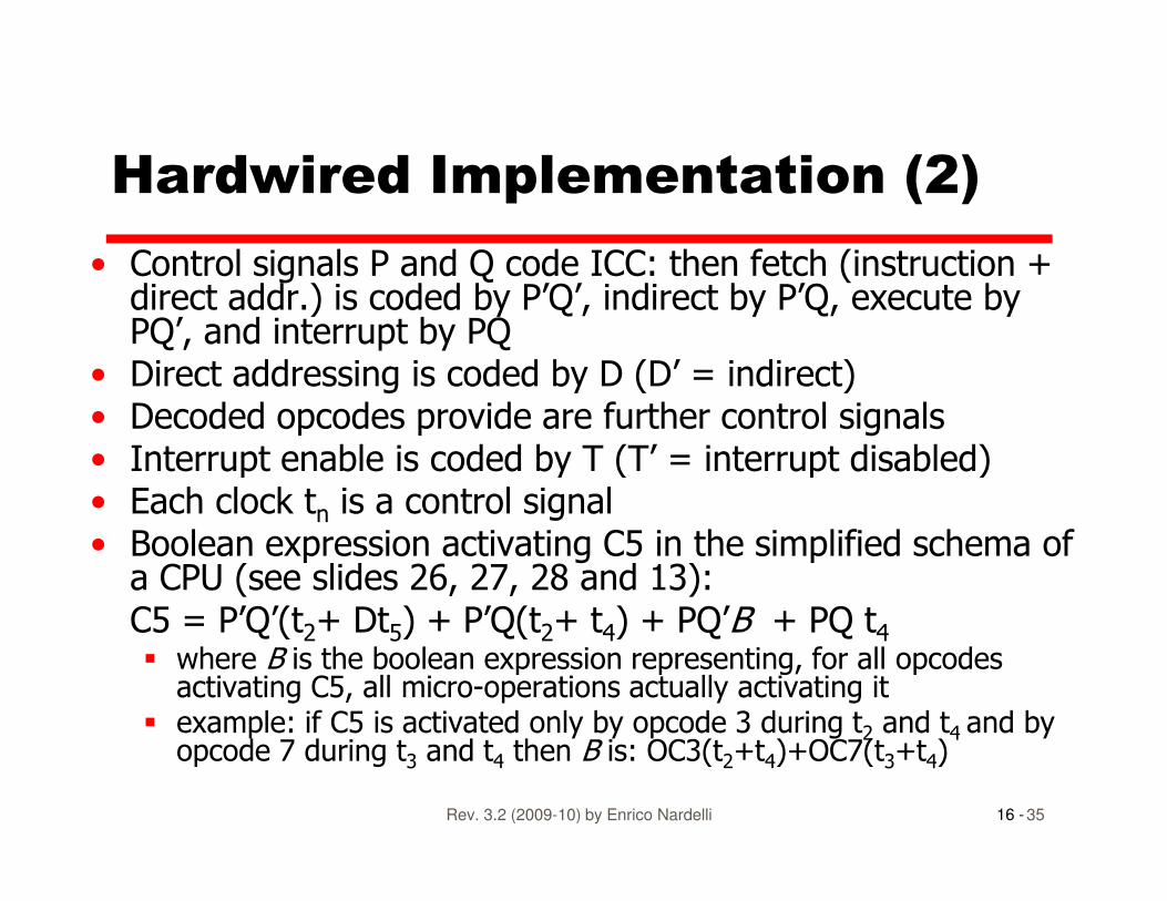
• Control signals P and Q code ICC: then fetch (instruction + direct addr.) is coded by P’Q’, indirect by P’Q, execute by PQ’, and interrupt by PQ
• Direct addressing is coded by D (D’ = indirect)• Decoded opcodes provide are further control signals• Interrupt enable is coded by T (T’ = interrupt disabled)
16 -Rev. 3.2 (2009-10) by Enrico Nardelli 35
• Interrupt enable is coded by T (T’ = interrupt disabled)• Each clock tn is a control signal• Boolean expression activating C5 in the simplified schema of a CPU (see slides 26, 27, 28 and 13):C5 = P’Q’(t2+ Dt5) + P’Q(t2+ t4) + PQ’B + PQ t4� where B is the boolean expression representing, for all opcodesactivating C5, all micro-operations actually activating it
� example: if C5 is activated only by opcode 3 during t2 and t4 and by opcode 7 during t3 and t4 then B is: OC3(t2+t4)+OC7(t3+t4)
Hardwired Implementation (3)
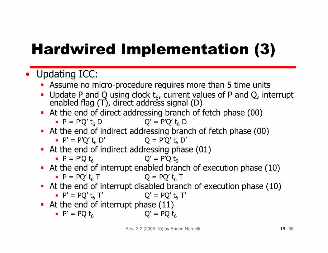
• Updating ICC:� Assume no micro-procedure requires more than 5 time units� Update P and Q using clock t6, current values of P and Q, interrupt enabled flag (T), direct address signal (D)
� At the end of direct addressing branch of fetch phase (00)• P = P’Q’ t6 D Q’ = P’Q’ t6 D
� At the end of indirect addressing branch of fetch phase (00)
16 -Rev. 3.2 (2009-10) by Enrico Nardelli 36
6 6
� At the end of indirect addressing branch of fetch phase (00)• P’ = P’Q’ t6 D’ Q = P’Q’ t6 D’
� At the end of indirect addressing phase (01)• P = P’Q t6 Q’ = P’Q t6
� At the end of interrupt enabled branch of execution phase (10)• P = PQ’ t6 T Q = PQ’ t6 T
� At the end of interrupt disabled branch of execution phase (10)• P’ = PQ’ t6 T’ Q’ = PQ’ t6 T’
� At the end of interrupt phase (11)• P’ = PQ t6 Q’ = PQ t6
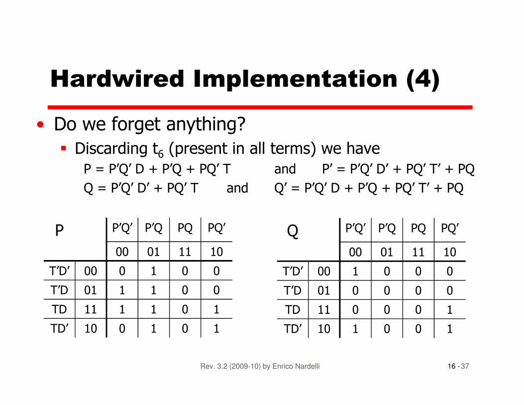
• Do we forget anything?
� Discarding t6 (present in all terms) we have
P = P’Q’ D + P’Q + PQ’ T and P’ = P’Q’ D’ + PQ’ T’ + PQ
Q = P’Q’ D’ + PQ’ T and Q’ = P’Q’ D + P’Q + PQ’ T’ + PQ
Hardwired Implementation (4)
16 -Rev. 3.2 (2009-10) by Enrico Nardelli 37
P P’Q’ P’Q PQ PQ’
00 01 11 10
T’D’ 00 0 1 0 0
T’D 01 1 1 0 0
TD 11 1 1 0 1
TD’ 10 0 1 0 1
Q P’Q’ P’Q PQ PQ’
00 01 11 10
T’D’ 00 1 0 0 0
T’D 01 0 0 0 0
TD 11 0 0 0 1
TD’ 10 1 0 0 1
Problems with the
Hardwired Implementation
• Complex sequencing & micro-operation logic
• Difficult to design and test
• Inflexible design
16 -Rev. 3.2 (2009-10) by Enrico Nardelli 38
• Difficult to add new instruction


![Sistemi Operativi [William Stallings]](https://static.fdocuments.in/doc/165x107/543cd117b1af9fc42e8b4811/sistemi-operativi-william-stallings.jpg)