William Stallings Computer Organization and Architecture 6th Edition
+
William Stallings
Computer Organization
and Architecture
10th Edition
© 2016 Pearson Education, Inc., Hoboken,
NJ. All rights reserved.
+ Chapter 4Cache Memory
© 2016 Pearson Education, Inc., Hoboken, NJ. All rights reserved.

Table 4.1
Key Characteristics of Computer Memory Systems
Location
Internal (e.g. processor registers, cache,
main memory)
External (e.g. optical disks, magnetic disks, tapes)
Capacity
Number of words
Number of bytes
Unit of Transfer
Word
Block Access Method
Sequential
Direct
Random
Associative
Performance
Access time
Cycle time
Transfer rate Physical Type
Semiconductor
Magnetic
Optical
Magneto-optical
Physical Characteristics
Volatile/nonvolatile Erasable/nonerasable
Organization
Memory modules
© 2016 Pearson Education, Inc., Hoboken, NJ. All rights reserved.
+Characteristics of Memory
Systems
◼ Location
◼ Refers to whether memory is internal and external to the computer
◼ Internal memory is often equated with main memory
◼ Processor requires its own local memory, in the form of registers
◼ Cache is another form of internal memory
◼ External memory consists of peripheral storage devices that are accessible to the processor via I/O controllers
◼ Capacity
◼ Memory is typically expressed in terms of bytes
◼ Unit of transfer
◼ For internal memory the unit of transfer is equal to the number of electrical lines into and out of the memory module
© 2016 Pearson Education, Inc., Hoboken, NJ. All rights reserved.

Method of Accessing Units of Data
Sequential access
Memory is organized into units of data called
records
Access must be made in a specific linear
sequence
Access time is variable
Direct access
Involves a shared read-write mechanism
Individual blocks or records have a unique
address based on physical location
Access time is variable
Random access
Each addressable location in memory has a unique, physically wired-in addressing mechanism
The time to access a given location is
independent of the sequence of prior
accesses and is constant
Any location can be selected at random and directly addressed and
accessed
Main memory and some cache systems are
random access
Associative
A word is retrieved based on a portion of its contents rather than its
address
Each location has its own addressing mechanism
and retrieval time is constant independent of location or prior access
patterns
Cache memories may employ associative
access
© 2016 Pearson Education, Inc., Hoboken, NJ. All rights reserved.

+ Memory◼ The most common forms are:
◼ Semiconductor memory
◼ Magnetic surface memory
◼ Optical
◼ Magneto-optical
◼ Several physical characteristics of data storage are important:
◼ Volatile memory
◼ Information decays naturally or is lost when electrical power is switched off
◼ Nonvolatile memory
◼ Once recorded, information remains without deterioration until deliberately changed
◼ No electrical power is needed to retain information
◼ Magnetic-surface memories
◼ Are nonvolatile
◼ Semiconductor memory
◼ May be either volatile or nonvolatile
◼ Nonerasable memory
◼ Cannot be altered, except by destroying the storage unit
◼ Semiconductor memory of this type is known as read-only memory (ROM)
◼ For random-access memory the organization is a key design issue
◼ Organization refers to the physical arrangement of bits to form words
© 2016 Pearson Education, Inc., Hoboken, NJ. All rights reserved.
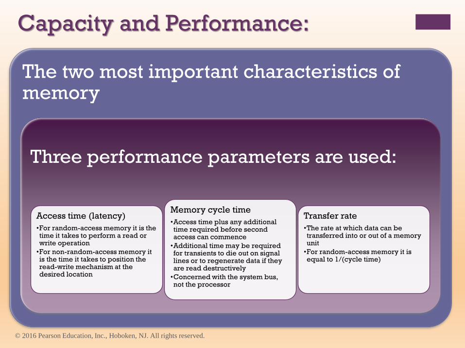
Capacity and Performance:
The two most important characteristics of memory
Three performance parameters are used:
Access time (latency)
•For random-access memory it is the time it takes to perform a read or write operation
•For non-random-access memory it is the time it takes to position the read-write mechanism at the desired location
Memory cycle time
•Access time plus any additional time required before second access can commence
•Additional time may be required for transients to die out on signal lines or to regenerate data if they are read destructively
•Concerned with the system bus, not the processor
Transfer rate
•The rate at which data can be transferred into or out of a memory unit
•For random-access memory it is equal to 1/(cycle time)
© 2016 Pearson Education, Inc., Hoboken, NJ. All rights reserved.

Chapter 8 <8> Digital Design and Computer Architecture: ARM® Edition © 2015
Processor MemoryAddress
MemWrite
WriteData
ReadData
WE
CLKCLK
Computer performance depends on:– Processor performance
– Memory system performance
Memory Interface
Introduction
Chapter 8 <9> Digital Design and Computer Architecture: ARM® Edition © 2015
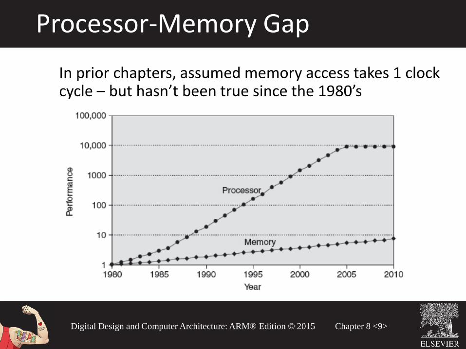
In prior chapters, assumed memory access takes 1 clock cycle – but hasn’t been true since the 1980’s
Processor-Memory Gap
Chapter 8 <10> Digital Design and Computer Architecture: ARM® Edition © 2015
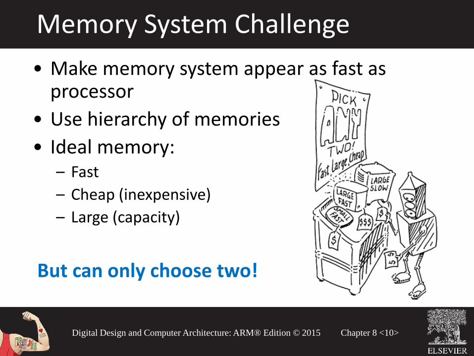
• Make memory system appear as fast as processor
• Use hierarchy of memories
• Ideal memory:– Fast
– Cheap (inexpensive)
– Large (capacity)
But can only choose two!
Memory System Challenge
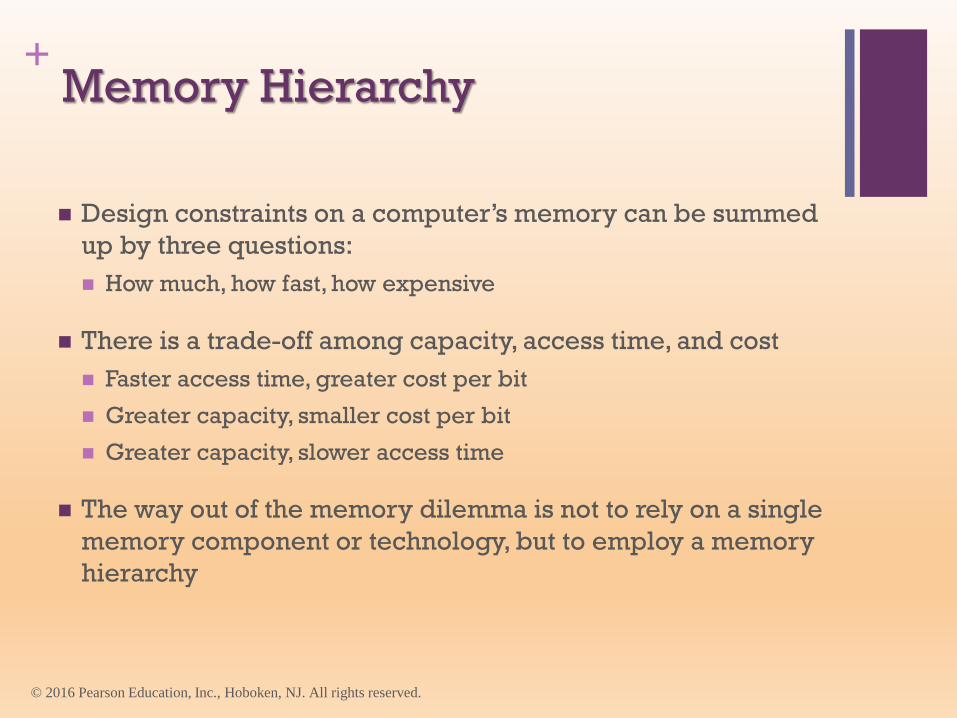
+Memory Hierarchy
◼ Design constraints on a computer’s memory can be summed
up by three questions:
◼ How much, how fast, how expensive
◼ There is a trade-off among capacity, access time, and cost
◼ Faster access time, greater cost per bit
◼ Greater capacity, smaller cost per bit
◼ Greater capacity, slower access time
◼ The way out of the memory dilemma is not to rely on a single
memory component or technology, but to employ a memory
hierarchy
© 2016 Pearson Education, Inc., Hoboken, NJ. All rights reserved.
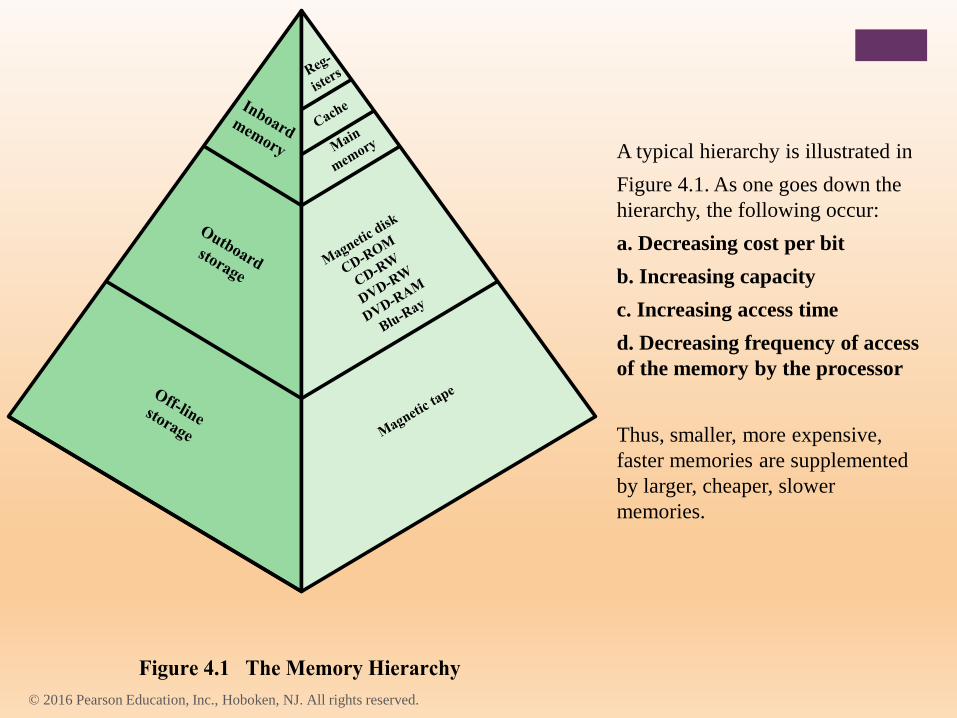
Figure 4.1 The Memory Hierarchy
Inboardmemory
Outboardstorage
Off-linestorage
Main
memory
Magnetic
disk
CD-ROM
CD-RW
DVD-RW
DVD-RAM
Blu-Ray
Magnetic
tape
Cache
Reg-
isters
© 2016 Pearson Education, Inc., Hoboken, NJ. All rights reserved.
A typical hierarchy is illustrated in
Figure 4.1. As one goes down the
hierarchy, the following occur:
a. Decreasing cost per bit
b. Increasing capacity
c. Increasing access time
d. Decreasing frequency of access
of the memory by the processor
Thus, smaller, more expensive,
faster memories are supplemented
by larger, cheaper, slower
memories.

Chapter 8 <13> Digital Design and Computer Architecture: ARM® Edition © 2015
Memory Hierarchy
Technology Price / GBAccess
Time (ns)
Bandwidth
(GB/s)
Cache
Main Memory
Virtual Memory
Capacity
Speed
SRAM $10,000 1
DRAM $10 10 - 50
SSD $1 100,000
25+
10
0.5
0.1HDD $0.1 10,000,000
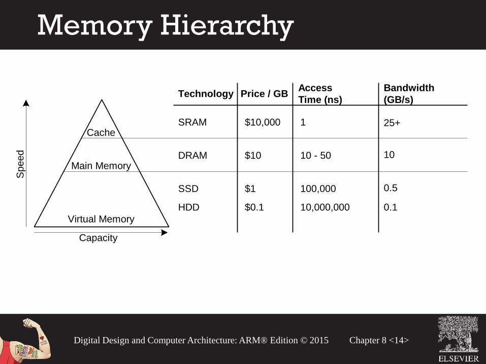
Chapter 8 <14> Digital Design and Computer Architecture: ARM® Edition © 2015
Memory Hierarchy
Technology Price / GBAccess
Time (ns)
Bandwidth
(GB/s)
Cache
Main Memory
Virtual Memory
Capacity
Speed
SRAM $10,000 1
DRAM $10 10 - 50
SSD $1 100,000
25+
10
0.5
0.1HDD $0.1 10,000,000

Chapter 8 <15> Digital Design and Computer Architecture: ARM® Edition © 2015
Exploit locality to make memory accesses fast
◼ Temporal Locality:
◼Locality in time
◼ If data used recently, likely to use it again soon
◼How to exploit: keep recently accessed data in
higher levels of memory hierarchy◼ Spatial Locality:
◼Locality in space
◼ If data used recently, likely to use nearby data
soon
◼How to exploit: when access data, bring nearby
data into higher levels of memory hierarchy too
Principle of Locality
Chapter 8 <16> Digital Design and Computer Architecture: ARM® Edition © 2015
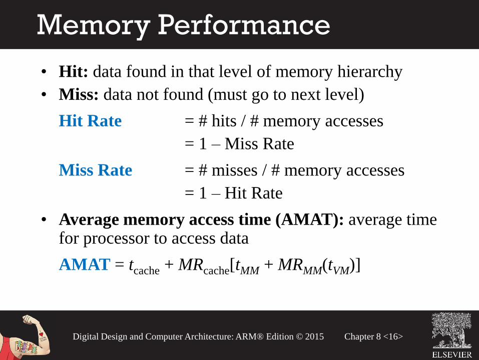
• Hit: data found in that level of memory hierarchy
• Miss: data not found (must go to next level)
Hit Rate = # hits / # memory accesses
= 1 – Miss Rate
Miss Rate = # misses / # memory accesses
= 1 – Hit Rate
• Average memory access time (AMAT): average time for processor to access data
AMAT = tcache + MRcache[tMM + MRMM(tVM)]
Memory Performance
Chapter 8 <17> Digital Design and Computer Architecture: ARM® Edition © 2015
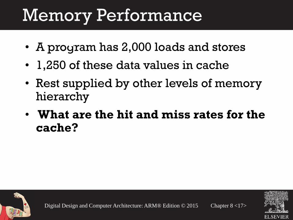
• A program has 2,000 loads and stores
• 1,250 of these data values in cache
• Rest supplied by other levels of memory hierarchy
• What are the hit and miss rates for the cache?
Memory Performance
Example 1

Chapter 8 <18> Digital Design and Computer Architecture: ARM® Edition © 2015
• A program has 2,000 loads and stores
• 1,250 of these data values in cache
• Rest supplied by other levels of memory hierarchy
• What are the hit and miss rates for the cache?
Hit Rate = 1250/2000 = 0.625
Miss Rate = 750/2000 = 0.375 = 1 – Hit Rate
Memory Performance
Example 1
Chapter 8 <19> Digital Design and Computer Architecture: ARM® Edition © 2015
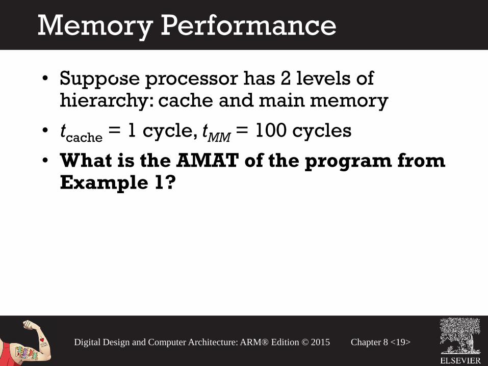
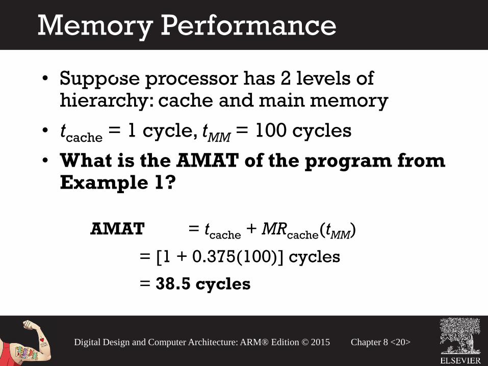
• Suppose processor has 2 levels of hierarchy: cache and main memory
• tcache = 1 cycle, tMM = 100 cycles
• What is the AMAT of the program from Example 1?
Memory Performance
Example 2
Chapter 8 <20> Digital Design and Computer Architecture: ARM® Edition © 2015
• Suppose processor has 2 levels of hierarchy: cache and main memory
• tcache = 1 cycle, tMM = 100 cycles
• What is the AMAT of the program from Example 1?
AMAT = tcache + MRcache(tMM)
= [1 + 0.375(100)] cycles
= 38.5 cycles
Memory Performance
Example 2
+Memory
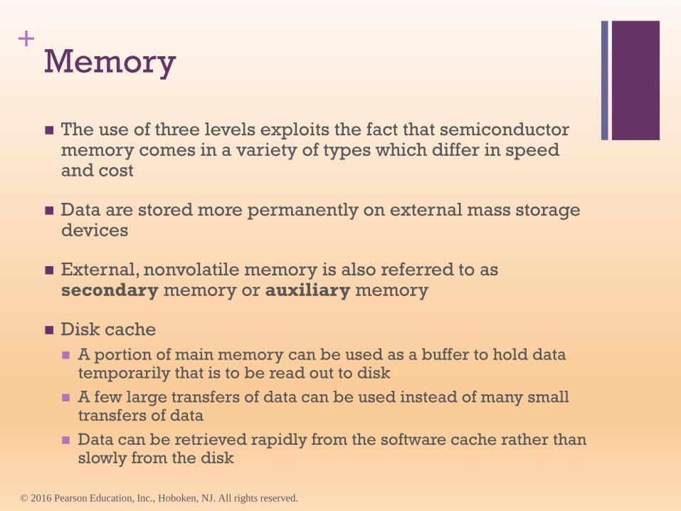
◼ The use of three levels exploits the fact that semiconductor memory comes in a variety of types which differ in speed and cost
◼ Data are stored more permanently on external mass storage devices
◼ External, nonvolatile memory is also referred to as secondary memory or auxiliary memory
◼ Disk cache
◼ A portion of main memory can be used as a buffer to hold data temporarily that is to be read out to disk
◼ A few large transfers of data can be used instead of many small transfers of data
◼ Data can be retrieved rapidly from the software cache rather than slowly from the disk
© 2016 Pearson Education, Inc., Hoboken, NJ. All rights reserved.
CPU
Word Transfer
Fast
Fastest FastLessfast
Slow
Slow
Block Transfer
Cache Main Memory
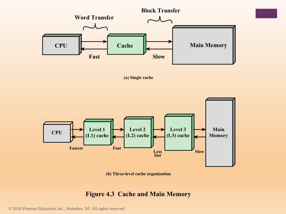
Figure 4.3 Cache and Main Memory
(a) Single cache
(b) Three-level cache organization
CPULevel 1
(L1) cache
Level 2
(L2) cache
Level 3
(L3) cache
Main
Memory
© 2016 Pearson Education, Inc., Hoboken, NJ. All rights reserved.
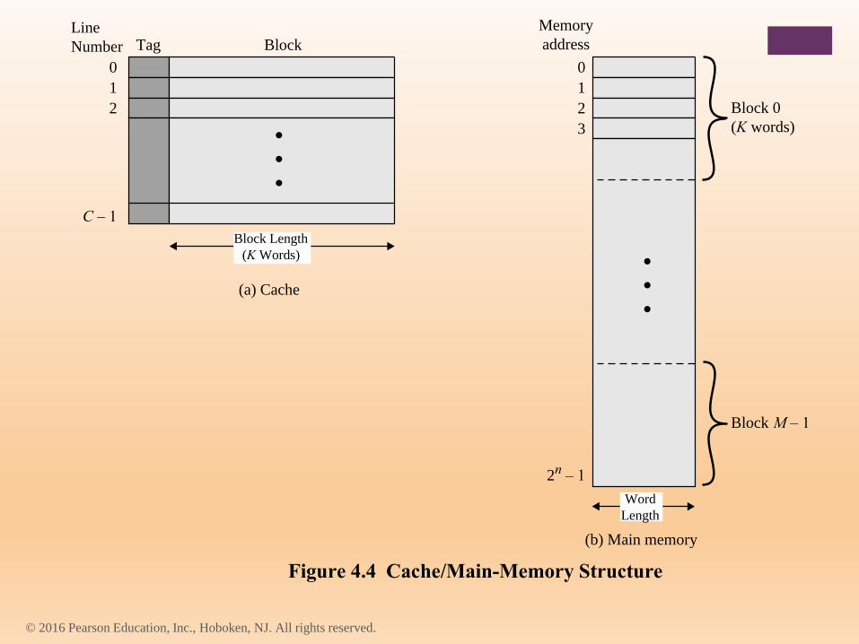
Memory
address
0
1
2
0
1
2
C – 1
3
2n – 1
Word
Length
Block Length
(K Words)
Block 0
(K words)
Block M – 1
Line
Number Tag Block
(b) Main memory
(a) Cache
Figure 4.4 Cache/Main-Memory Structure
© 2016 Pearson Education, Inc., Hoboken, NJ. All rights reserved.
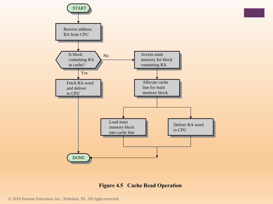
Receive address
RA from CPU
Is block
containing RA
in cache?
Fetch RA word
and deliver
to CPU
DONE
Access main
memory for block
containing RA
Allocate cache
line for main
memory block
Deliver RA word
to CPU
Load main
memory block
into cache line
Figure 4.5 Cache Read Operation
START
No
Yes
© 2016 Pearson Education, Inc., Hoboken, NJ. All rights reserved.
Processor Cache
Address
Address
buffer
Data
buffer
Control
Data
Figure 4.6 Typical Cache Organization
Control
Syst
em B
us
© 2016 Pearson Education, Inc., Hoboken, NJ. All rights reserved.

Table 4.2
Elements of Cache Design
Cache Addresses
Logical
Physical
Cache Size Mapping Function
Direct
Associative
Set Associative
Replacement Algorithm
Least recently used (LRU)
First in first out (FIFO) Least frequently used (LFU)
Random
Write Policy
Write through
Write back
Line Size Number of caches
Single or two level
Unified or split
© 2016 Pearson Education, Inc., Hoboken, NJ. All rights reserved.
+Cache Addresses
◼ Virtual memory
◼ Facility that allows programs to address memory from a logical
point of view, without regard to the amount of main memory
physically available
◼ When used, the address fields of machine instructions contain
virtual addresses
◼ For reads to and writes from main memory, a hardware memory
management unit (MMU) translates each virtual address into a
physical address in main memory
Virtual Memory
© 2016 Pearson Education, Inc., Hoboken, NJ. All rights reserved.
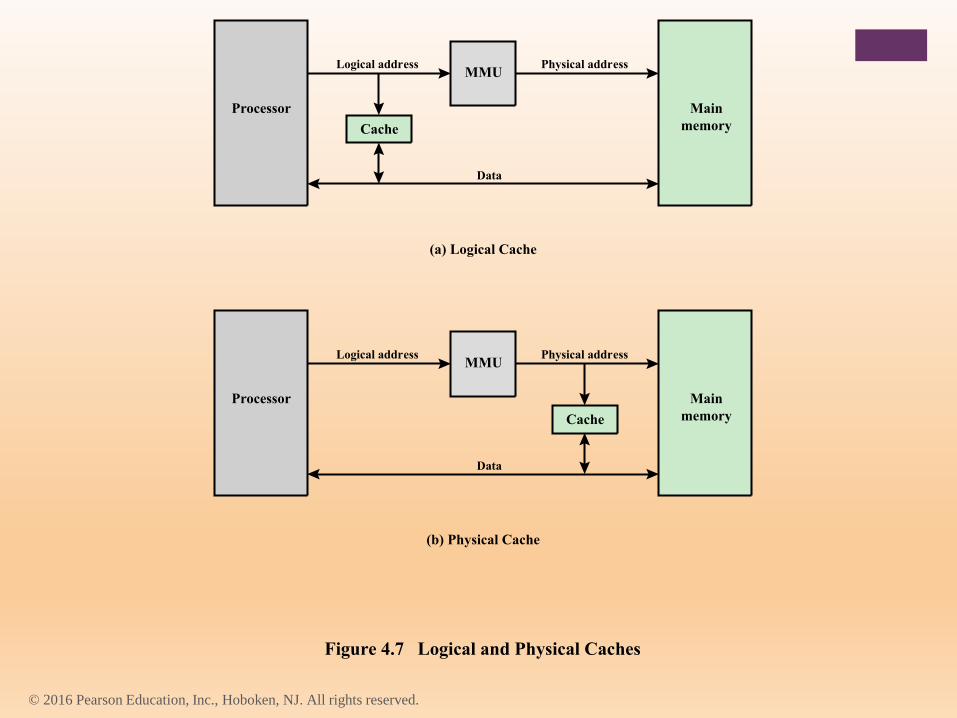
Processor Main
memoryCache
Logical address Physical address
Data
MMU
(a) Logical Cache
Processor Main
memoryCache
Logical address Physical address
Data
MMU
(b) Physical Cache
Figure 4.7 Logical and Physical Caches
© 2016 Pearson Education, Inc., Hoboken, NJ. All rights reserved.
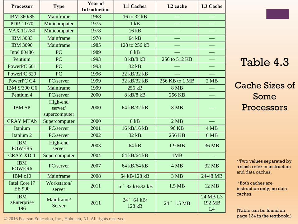
Table 4.3
Cache Sizes of
Some
Processors
a Two values separated by
a slash refer to instruction
and data caches.
b Both caches are
instruction only; no data
caches.
(Table can be found on
page 134 in the textbook.)
Processor Type Year of
Introduction L1 Cachea L2 cache L3 Cache
IBM 360/85 Mainframe 1968 16 to 32 kB — —
PDP-11/70 Minicomputer 1975 1 kB — —
VAX 11/780 Minicomputer 1978 16 kB — —
IBM 3033 Mainframe 1978 64 kB — —
IBM 3090 Mainframe 1985 128 to 256 kB — —
Intel 80486 PC 1989 8 kB — —
Pentium PC 1993 8 kB/8 kB 256 to 512 KB —
PowerPC 601 PC 1993 32 kB — —
PowerPC 620 PC 1996 32 kB/32 kB — —
PowerPC G4 PC/server 1999 32 kB/32 kB 256 KB to 1 MB 2 MB
IBM S/390 G6 Mainframe 1999 256 kB 8 MB —
Pentium 4 PC/server 2000 8 kB/8 kB 256 KB —
IBM SP High-end
server/
supercomputer
2000 64 kB/32 kB 8 MB —
CRAY MTAb Supercomputer 2000 8 kB 2 MB —
Itanium PC/server 2001 16 kB/16 kB 96 KB 4 MB
Itanium 2 PC/server 2002 32 kB 256 KB 6 MB
IBM POWER5
High-end server
2003 64 kB 1.9 MB 36 MB
CRAY XD-1 Supercomputer 2004 64 kB/64 kB 1MB —
IBM POWER6
PC/server 2007 64 kB/64 kB 4 MB 32 MB
IBM z10 Mainframe 2008 64 kB/128 kB 3 MB 24-48 MB
Intel Core i7 EE 990
Workstaton/
server 2011 6 ´ 32 kB/32 kB 1.5 MB 12 MB
IBM zEnterprise
196
Mainframe/
Server 2011
24 ´ 64 kB/
128 kB 24 ´ 1.5 MB
24 MB L3
192 MB
L4
© 2016 Pearson Education, Inc., Hoboken, NJ. All rights reserved.
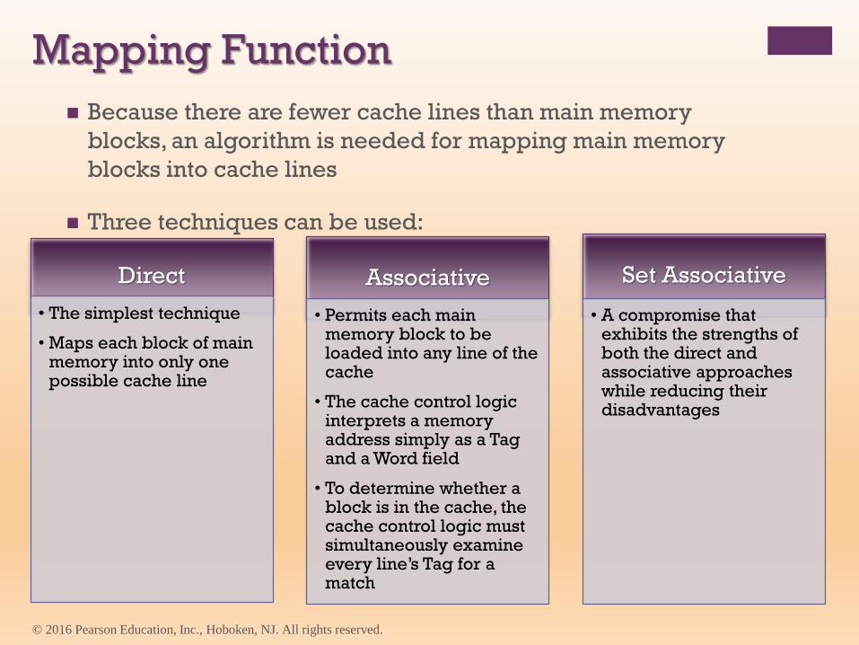
Mapping Function
◼ Because there are fewer cache lines than main memory
blocks, an algorithm is needed for mapping main memory
blocks into cache lines
◼ Three techniques can be used:
Direct
• The simplest technique
• Maps each block of main memory into only one possible cache line
Associative
• Permits each main memory block to be loaded into any line of the cache
• The cache control logic interprets a memory address simply as a Tag and a Word field
• To determine whether a block is in the cache, the cache control logic must simultaneously examine every line’s Tag for a match
Set Associative
• A compromise that exhibits the strengths of both the direct and associative approaches while reducing their disadvantages
© 2016 Pearson Education, Inc., Hoboken, NJ. All rights reserved.

+Replacement Algorithms
◼ Once the cache has been filled, when a new block is brought
into the cache, one of the existing blocks must be replaced
◼ For direct mapping there is only one possible line for any
particular block and no choice is possible
◼ For the associative and set-associative techniques a
replacement algorithm is needed
◼ To achieve high speed, an algorithm must be implemented in
hardware
© 2016 Pearson Education, Inc., Hoboken, NJ. All rights reserved.

+ The most common replacement
algorithms are:
◼ Least recently used (LRU)
◼ Most effective
◼ Replace that block in the set that has been in the cache longest with no reference to it
◼ Because of its simplicity of implementation, LRU is the most popular replacement algorithm
◼ First-in-first-out (FIFO)
◼ Replace that block in the set that has been in the cache longest
◼ Easily implemented as a round-robin or circular buffer technique
◼ Least frequently used (LFU)
◼ Replace that block in the set that has experienced the fewest references
◼ Could be implemented by associating a counter with each line
© 2016 Pearson Education, Inc., Hoboken, NJ. All rights reserved.
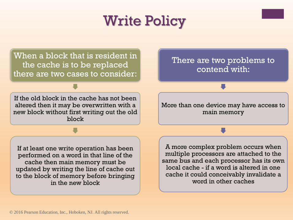
When a block that is resident in the cache is to be replaced
there are two cases to consider:
If the old block in the cache has not been altered then it may be overwritten with a new block without first writing out the old
block
If at least one write operation has been performed on a word in that line of the
cache then main memory must be updated by writing the line of cache out to the block of memory before bringing
in the new block
There are two problems to contend with:
More than one device may have access to main memory
A more complex problem occurs when multiple processors are attached to the
same bus and each processor has its own local cache - if a word is altered in one cache it could conceivably invalidate a
word in other caches
Write Policy
© 2016 Pearson Education, Inc., Hoboken, NJ. All rights reserved.
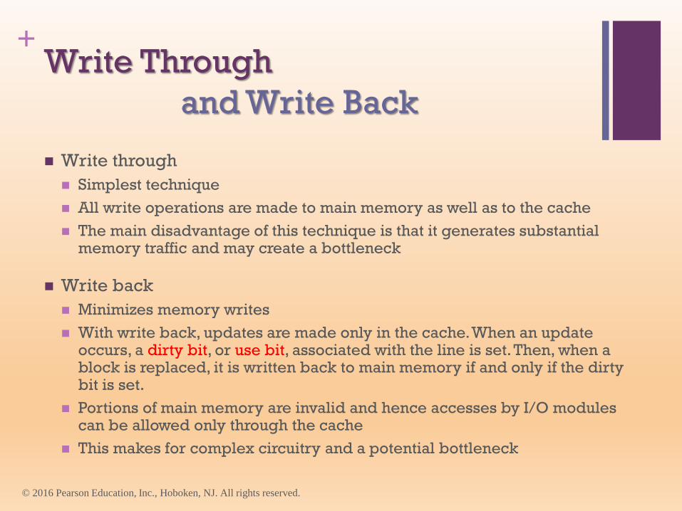
+Write Through
and Write Back
◼ Write through
◼ Simplest technique
◼ All write operations are made to main memory as well as to the cache
◼ The main disadvantage of this technique is that it generates substantial memory traffic and may create a bottleneck
◼ Write back
◼ Minimizes memory writes
◼ With write back, updates are made only in the cache. When an update occurs, a dirty bit, or use bit, associated with the line is set. Then, when a block is replaced, it is written back to main memory if and only if the dirty bit is set.
◼ Portions of main memory are invalid and hence accesses by I/O modules can be allowed only through the cache
◼ This makes for complex circuitry and a potential bottleneck
© 2016 Pearson Education, Inc., Hoboken, NJ. All rights reserved.
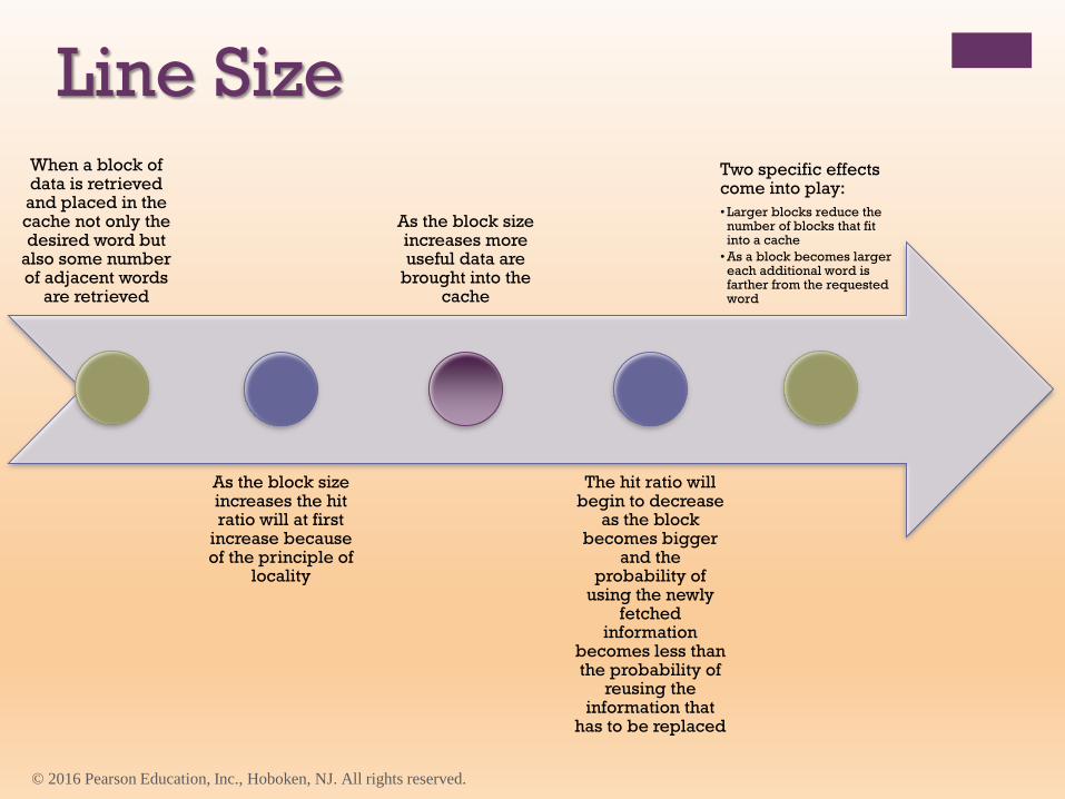
Line SizeWhen a block of data is retrieved and placed in the cache not only the desired word but
also some number of adjacent words
are retrieved
As the block size increases the hit ratio will at first
increase because of the principle of
locality
As the block size increases more useful data are
brought into the cache
The hit ratio will begin to decrease
as the block becomes bigger
and the probability of
using the newly fetched
information becomes less than the probability of
reusing the information that
has to be replaced
Two specific effects come into play:
• Larger blocks reduce the number of blocks that fit into a cache
• As a block becomes larger each additional word is farther from the requested word
© 2016 Pearson Education, Inc., Hoboken, NJ. All rights reserved.
+Multilevel Caches
◼ As logic density has increased it has become possible to have a cache on the same chip as the processor
◼ The on-chip cache reduces the processor’s external bus activity and speeds up execution time and increases overall system performance
◼ When the requested instruction or data is found in the on-chip cache, the bus access is eliminated
◼ On-chip cache accesses will complete appreciably faster than would even zero-wait state bus cycles
◼ During this period the bus is free to support other transfers
◼ Two-level cache:
◼ Internal cache designated as level 1 (L1)
◼ External cache designated as level 2 (L2)
◼ Potential savings due to the use of an L2 cache depends on the hit rates in both the L1 and L2 caches
◼ The use of multilevel caches complicates all of the design issues related to caches, including size, replacement algorithm, and write policy
© 2016 Pearson Education, Inc., Hoboken, NJ. All rights reserved.
0.78
0.80
0.82
0.84
0.86
0.88
0.90
0.92
0.94
0.96
0.98
1k 2k 4k 8k 16k 32k
L1 = 16k
64k 128k 256k 512k 1M 2M
Hit
ra
tio
L2 Cache size (bytes)
L1 = 8k
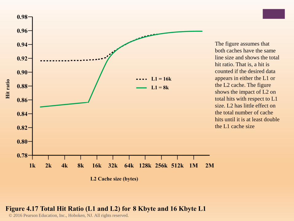
Figure 4.17 Total Hit Ratio (L1 and L2) for 8 Kbyte and 16 Kbyte L1© 2016 Pearson Education, Inc., Hoboken, NJ. All rights reserved.
The figure assumes that
both caches have the same
line size and shows the total
hit ratio. That is, a hit is
counted if the desired data
appears in either the L1 or
the L2 cache. The figure
shows the impact of L2 on
total hits with respect to L1
size. L2 has little effect on
the total number of cache
hits until it is at least double
the L1 cache size
+Unified Versus Split Caches
◼ Has become common to split cache:
◼ One dedicated to instructions
◼ One dedicated to data
◼ Both exist at the same level, typically as two L1 caches
◼ Advantages of unified cache:
◼ Higher hit rate
◼ Balances load of instruction and data fetches automatically
◼ Only one cache needs to be designed and implemented
◼ Trend is toward split caches at the L1 and unified caches for higher levels
◼ Advantages of split cache:
◼ Eliminates cache contention between instruction fetch/decode unit and execution unit
◼ Important in pipelining
© 2016 Pearson Education, Inc., Hoboken, NJ. All rights reserved.
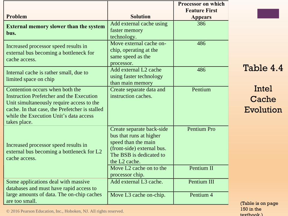
Problem Solution
Processor on which
Feature First
Appears
External memory slower than the system
bus.
Add external cache using
faster memory
technology.
386
Increased processor speed results in
external bus becoming a bottleneck for
cache access.
Move external cache on-
chip, operating at the
same speed as the
processor.
486
Internal cache is rather small, due to
limited space on chip
Add external L2 cache
using faster technology
than main memory
486
Contention occurs when both the
Instruction Prefetcher and the Execution
Unit simultaneously require access to the
cache. In that case, the Prefetcher is stalled
while the Execution Unit’s data access takes place.
Create separate data and
instruction caches.
Pentium
Create separate back-side
bus that runs at higher
speed than the main (front-side) external bus.
The BSB is dedicated to
the L2 cache.
Pentium Pro
Increased processor speed results in
external bus becoming a bottleneck for L2
cache access.
Move L2 cache on to the
processor chip.
Pentium II
Add external L3 cache. Pentium III
Some applications deal with massive
databases and must have rapid access to large amounts of data. The on-chip caches
are too small. Move L3 cache on-chip. Pentium 4
Table 4.4
Intel
Cache
Evolution
(Table is on page
150 in the
textbook.)© 2016 Pearson Education, Inc., Hoboken, NJ. All rights reserved.
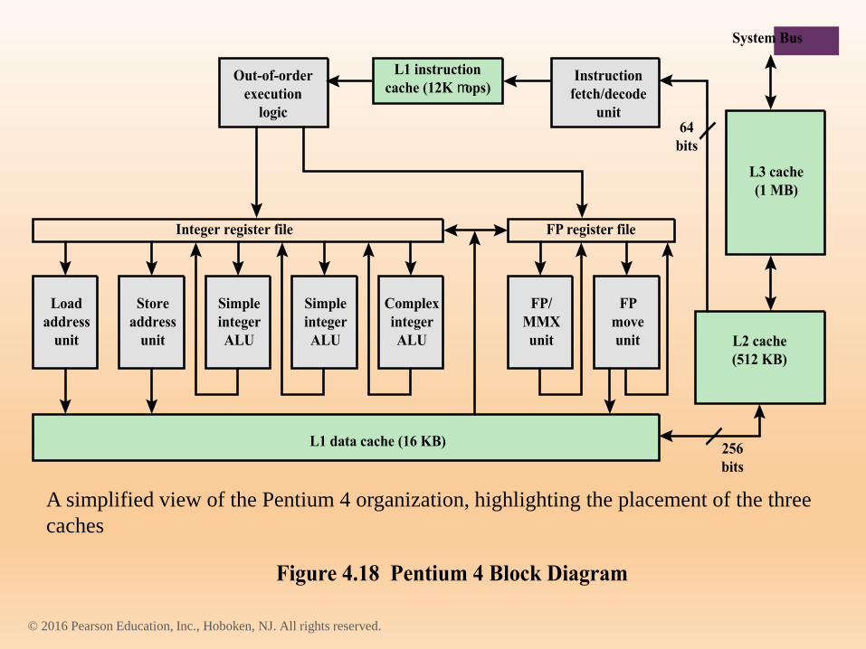
Figure 4.18 Pentium 4 Block Diagram
Load
address
unit
Integer register file
L1 data cache (16 KB)
FP register file
Store
address
unit
Simple
integer
ALU
Instruction
fetch/decode
unit
Out-of-order
execution
logic
L2 cache
(512 KB)
L3 cache
(1 MB)
L1 instruction
cache (12K mops)
Simple
integer
ALU
Complex
integer
ALU
FP/
MMX
unit
FP
move
unit
System Bus
64
bits
256
bits
© 2016 Pearson Education, Inc., Hoboken, NJ. All rights reserved.
A simplified view of the Pentium 4 organization, highlighting the placement of the three
caches

Table 4.5 Pentium 4 Cache Operating Modes
Control Bits Operating Mode
CD NW Cache Fills Write Throughs Invalidates
0 0 Enabled Enabled Enabled
1 0 Disabled Enabled Enabled
1 1 Disabled Disabled Disabled
Note: CD = 0; NW = 1 is an invalid combination.
© 2016 Pearson Education, Inc., Hoboken, NJ. All rights reserved.
The L1 data cache is controlled by two bits in one of the control registers, labeled the CD
(cache disable) and NW (not write-through) bits (Table 4.5). There are also two Pentium 4
instructions that can be used to control the data cache: INVD invalidates (flushes) the internal
cache memory and signals the external cache (if any) to invalidate. WBINVD writes back and
invalidates internal cache and then writes back and invalidates external cache.
+ Summary
◼ Computer memory
system overview
◼ Characteristics of
Memory Systems
◼ Memory Hierarchy
◼ Cache memory
principles
◼ Pentium 4 cache
organization
◼ Elements of cache
design
◼ Cache addresses
◼ Cache size
◼ Mapping function
◼ Replacement algorithms
◼ Write policy
◼ Line size
◼ Number of caches
Chapter 4
Cache
Memory
© 2016 Pearson Education, Inc., Hoboken, NJ. All rights reserved.