Various misfit dislocations in green
5
Transcript of Various misfit dislocations in green

Phys. Status Solidi A 207, No. 6, 1305–1308 (2010) / DOI 10.1002/pssa.200983645 p s sa
statu
s
soli
di
www.pss-a.comph
ysi
ca
applications and materials science
Various misfit dislocations in green
and yellow GaInN/GaN light emitting diodesMingwei Zhu*,1, Shi You1, Theeradetch Detchprohm1, Tanya Paskova2, Edward A. Preble2,and Christian Wetzel**,1
1 Future Chips Constellation, Department of Physics, Applied Physics, and Astronomy, Rensselaer Polytechnic Institute, Troy,
NY 12180, USA2 Kyma Technologies Inc., 8829 Midway West Road, Raleigh, NC 27617, USA
Received 16 October 2009, accepted 7 March 2010
Published online 17 May 2010
Keywords dislocations, electroluminescence, GaInN/GaN, LEDs, MOVPE
* Corresponding author: e-mail [email protected], Phone: þ1 518 276 2814, Fax: þ1 518 276 8042** e-mail [email protected]
We report the growth and structural characteristics of green and
yellow (529–576 nm) GaInN/GaN light emitting diodes (LEDs)
grown on two types of c-plane substrates – bulk GaN and
sapphire. In this longer wavelength range, depending on the
substrate, we find different strain relaxation mechanisms within
the GaInN/GaN quantum well (QW) region. In optimized
epitaxy, structures on sapphire that contain a low density of
threading dislocations (TDs) within the n-GaN show virtually
no generation of additional misfit dislocations (MDs)
(<108 cm�2) or V-defects within the QW region for emission
wavelengths up to 571 nm. On bulk GaN substrate, however,
where much fewer TDs reach the QWs, strain relaxation is
observed by inclined dislocation pairs in green emitters and a
high density of edge-type MDs in yellow emitters. The
electroluminescence line width, as well as the efficiency droop,
was found to increase with dislocation density in the QWs.
� 2010 WILEY-VCH Verlag GmbH & Co. KGaA, Weinheim
1 Introduction Green and yellow GaInN/GaN lightemitting diodes (LEDs) are essential components forenergy-efficient RGB and RGBY solid-state white lightingwith good color rendering and high customer satisfaction.Efficiency in that range, however, is still below that ofGaInN-based blue and AlGaInP-based red emitters. Thechallenge in closing this ‘‘green gap’’ lies in the incorpora-tion of sufficient InN into the GaInN quantum wells (QWs)of the active region without degrading the crystallineperfection and epitaxial homogeneity [1]. Here, yellowemitters pose an even higher challenge than the green ones.They require management of higher biaxial strain withinthis lattice mismatched system and its propensity for defectgeneration, such as misfit dislocations (MDs) [2] and V-defect [3] formation. For heteroepitaxy on sapphire, theactive region will have to be grown on layers that alreadycontain a high density network of threading dislocations(TDs) on the order 108–109 cm�2. Our earlier work hasshown that all such defects need to be avoided or reduced toboost LED efficiency, particularly in the longer wavelengthregions of green [1], and likely also in the yellow. Bulk GaNsubstrates, obtained by hydride vapor phase epitaxy (HVPE)
[4], prove a solution due to dislocation densities as low as5� 106 cm�2.
Here we compare LEDs grown on bulk GaN andsapphire substrates with emission wavelength from greento yellow (529–576 nm). We characterize the structural pro-perties by means of cross-sectional transmission electronmicroscopy (TEM) and LED performance by electrolumi-nescence (EL) spectroscopy.
2 Experimental Two types of c-axis grown c-planeGaN templates were used in this study: bulk GaN and5-mm-thick GaN on c-plane sapphire. The bulk GaNsubstrates of size 1 cm� 1 cm were obtained by HVPE andhave a dislocation density as low as 5� 106 cm�2. Bothtemplates have a surface roughness of 0.1–0.2 nm (root meansquare), as measured by atomic force microscopy. LEDstructures were grown on both templates by metalorganicvapor phase epitaxy. Growth conditions were adopted tosuppress V-defect generation [5, 6]. Active regions consist-ing of 8 or 10 pairs of GaInN/GaN QWs were sandwichedbetween the 1-mm-thick overgrown n-GaN and 180-nm-thick p-GaN. The normal QW and barrier thicknesses are 3
� 2010 WILEY-VCH Verlag GmbH & Co. KGaA, Weinheim
1306 M. Zhu et al.: Various misfit dislocations in green and yellow GaInN/GaN LEDsp
hys
ica ssp st
atu
s
solid
i a
and 20–25 nm, respectively. A 15-nm-thick Al0.18Ga0.82Nelectron blocking layer was inserted between the last barrierand the p-GaN. EL of the full LED epi wafer was char-acterized using scratch diodes with 1 mm diameter indiumcontacts. LEDs with peak emission wavelengths from529 nm (green) to 576 nm (yellow) at 20 mA (current density2.5 A/cm2) are included in this study. As determined by X-ray diffraction, the average InN fraction in the QW rangesfrom 8 to 12%, though we are aware that other groups quotehigher numbers to reach these wavelength ranges [7]. Smallsample portions were prepared for TEM analysis by standardmechanical polishing and low angle ion milling at 5 kV.Bright field and high-resolution TEM images were recordedon PHILIPS CM12 TEM (120 kV) and JEOL 2010 TEM(200 kV).
3 Results and discussion We generally find thatemission wavelength is shorter in LEDs on bulk GaN than onsapphire even when grown in the same run. At 529 nm onbulk, the difference is around 30 nm. The X-ray diffractionmeasurement shows a lower InN-fraction. This may becaused by the higher thermal conductivity and lower waferbowing in bulk GaN, resulting in a higher surface growthtemperature. The TEM analysis also reveals substantiallydifferent dislocation networks in both structures at such longwavelengths.
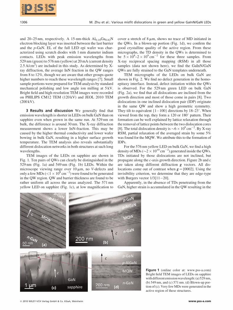
TEM images of the LEDs on sapphire are shown inFig. 1. Ten pairs of QWs can clearly be distinguished in the529 nm (Fig. 1a) and 549 nm (Fig. 1b) LEDs. Within themicroscope viewing range over 10mm, no V-defects andonly a few MDs (<1� 108 cm�2) were found to be generatedin the QW region. QW and barrier thickness are found to berather uniform all across the areas analyzed. The 571 nmyellow LED on sapphire (Fig. 1c), at low magnification to
� 2010 WILEY-VCH Verlag GmbH & Co. KGaA, Weinheim
cover a stretch of 8mm, shows no trace of MD initiated inthe QWs. In a blown-up portion (Fig. 1d), we confirm thegood crystalline quality of the active region. From thesemicrographs, the TD density in the QWs is determined tobe 5� 108–2� 109 cm�2 for these three samples. FromX-ray reciprocal spacing mapping (RSM) in all thosesamples (data not shown here), we find the GaInN/GaNQWs are fully strained to the GaN templates underneath.
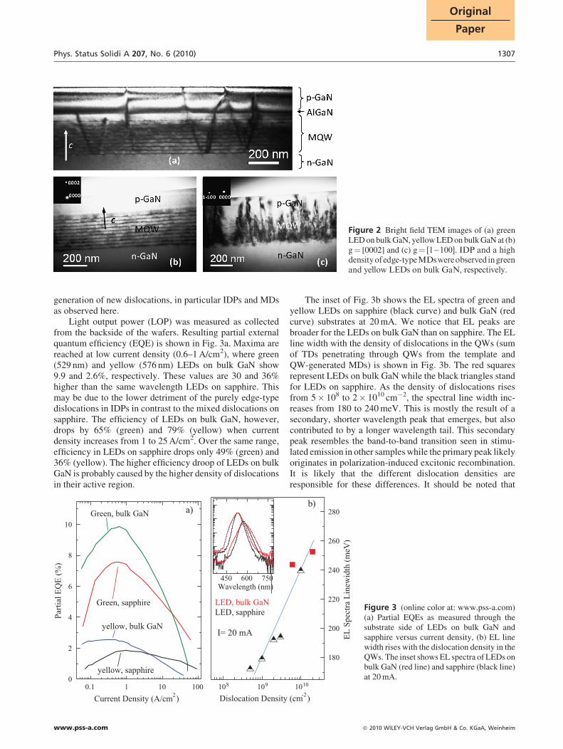
TEM micrographs of the LEDs on bulk GaN areshown in Fig. 2. We find no defect generation in the homo-epitaxy interface. Instead, defect initiation within the QWsis observed. For the 529 nm green LED on bulk GaN(Fig. 2a), we find that all dislocations are inclined from thegrowth direction and most of those come in pairs [8]. Twodislocations in one inclined dislocation pair (IDP) originatein the same QW and show a high geometric symmetry.They tilt to equivalent {1�100} directions by 18–238. Whenviewed from the top, they form a 120 or 1808 pattern. Theirformation can be well explained by lattice relaxation throughthe removal of lattice points between the two dislocation cores[8]. The total dislocation density is �6� 109 cm�2. By X-rayRSM, partial relaxation of the averaged strain by some 5%was found for the MQW. We attribute this to the formation ofIDPs.
For the 576 nm yellow LED on bulk GaN, we find a highdensity of MDs (�2� 1010 cm�2) generated inside the QWs.TDs initiated by those dislocations are not inclined, butpropagate along the c-axis growth direction. Figure 2b and care taken along different diffraction g vectors. All dis-locations come out of contrast when g¼ [0002]. Using theinvisibility criterion, we determine that they are edge-typewith Burgers vector 1/3[11�20].
Apparently, in the absence of TDs penetrating from theGaN, higher strain is accumulated in the QW resulting in the
Figure 1 (online color at: www.pss-a.com)Bright field TEM images of LEDs on sapphirewithdifferentemissionwavelength: (a)529 nm,(b) 549 nm, and (c) 571 nm. (d) Blown-up por-tion of (c). Very few MDs were generated in theactive region of these structures.
www.pss-a.com
Phys. Status Solidi A 207, No. 6 (2010) 1307
Original
Paper
Figure 2 Bright field TEM images of (a) greenLED on bulk GaN, yellow LED on bulk GaN at (b)g¼ [0002] and (c) g¼ [1�100]. IDP and a highdensityofedge-typeMDswereobserved ingreenand yellow LEDs on bulk GaN, respectively.
generation of new dislocations, in particular IDPs and MDsas observed here.
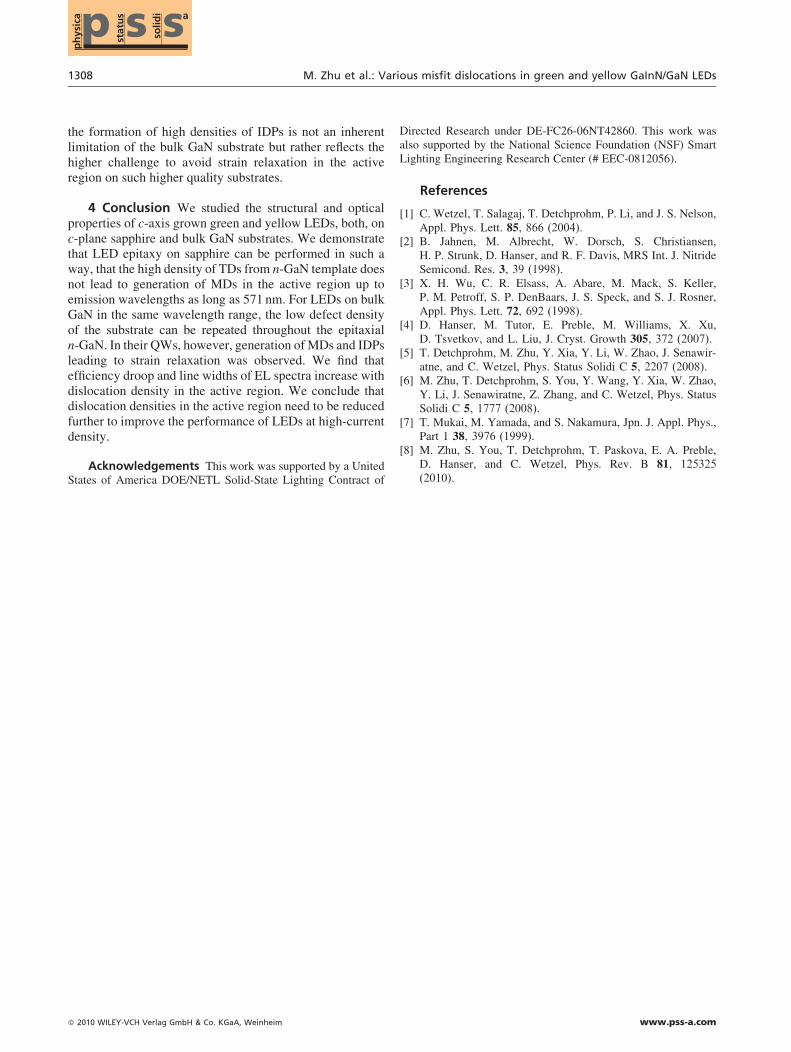
Light output power (LOP) was measured as collectedfrom the backside of the wafers. Resulting partial externalquantum efficiency (EQE) is shown in Fig. 3a. Maxima arereached at low current density (0.6–1 A/cm2), where green(529 nm) and yellow (576 nm) LEDs on bulk GaN show9.9 and 2.6%, respectively. These values are 30 and 36%higher than the same wavelength LEDs on sapphire. Thismay be due to the lower detriment of the purely edge-typedislocations in IDPs in contrast to the mixed dislocations onsapphire. The efficiency of LEDs on bulk GaN, however,drops by 65% (green) and 79% (yellow) when currentdensity increases from 1 to 25 A/cm2. Over the same range,efficiency in LEDs on sapphire drops only 49% (green) and36% (yellow). The higher efficiency droop of LEDs on bulkGaN is probably caused by the higher density of dislocationsin their active region.
1001010.10
2
4
6
8
10
yellow, sapphire
yellow, bulk GaN
Green, sapphire
Parti
al E
QE
(%)
Current Density (A/cm2)
Green, bulk GaN
108 109
Dislocation Density
750600450Wavelength (nm)
LED, bulk GaNLED, sapphire
I= 20 mA
a)
www.pss-a.com
The inset of Fig. 3b shows the EL spectra of green andyellow LEDs on sapphire (black curve) and bulk GaN (redcurve) substrates at 20 mA. We notice that EL peaks arebroader for the LEDs on bulk GaN than on sapphire. The ELline width with the density of dislocations in the QWs (sumof TDs penetrating through QWs from the template andQW-generated MDs) is shown in Fig. 3b. The red squaresrepresent LEDs on bulk GaN while the black triangles standfor LEDs on sapphire. As the density of dislocations risesfrom 5� 108 to 2� 1010 cm�2, the spectral line width inc-reases from 180 to 240 meV. This is mostly the result of asecondary, shorter wavelength peak that emerges, but alsocontributed to by a longer wavelength tail. This secondarypeak resembles the band-to-band transition seen in stimu-lated emission in other samples while the primary peak likelyoriginates in polarization-induced excitonic recombination.It is likely that the different dislocation densities areresponsible for these differences. It should be noted that
1010
180
200
220
240
260
280
EL
Spec
tra L
inew
idth
(meV
)
(cm-2)
b)
Figure 3 (online color at: www.pss-a.com)(a) Partial EQEs as measured through thesubstrate side of LEDs on bulk GaN andsapphire versus current density, (b) EL linewidth rises with the dislocation density in theQWs. The inset shows EL spectra of LEDs onbulk GaN (red line) and sapphire (black line)at 20 mA.
� 2010 WILEY-VCH Verlag GmbH & Co. KGaA, Weinheim
1308 M. Zhu et al.: Various misfit dislocations in green and yellow GaInN/GaN LEDsp
hys
ica ssp st
atu
s
solid
i a
the formation of high densities of IDPs is not an inherentlimitation of the bulk GaN substrate but rather reflects thehigher challenge to avoid strain relaxation in the activeregion on such higher quality substrates.
4 Conclusion We studied the structural and opticalproperties of c-axis grown green and yellow LEDs, both, onc-plane sapphire and bulk GaN substrates. We demonstratethat LED epitaxy on sapphire can be performed in such away, that the high density of TDs from n-GaN template doesnot lead to generation of MDs in the active region up toemission wavelengths as long as 571 nm. For LEDs on bulkGaN in the same wavelength range, the low defect densityof the substrate can be repeated throughout the epitaxialn-GaN. In their QWs, however, generation of MDs and IDPsleading to strain relaxation was observed. We find thatefficiency droop and line widths of EL spectra increase withdislocation density in the active region. We conclude thatdislocation densities in the active region need to be reducedfurther to improve the performance of LEDs at high-currentdensity.
Acknowledgements This work was supported by a UnitedStates of America DOE/NETL Solid-State Lighting Contract of
� 2010 WILEY-VCH Verlag GmbH & Co. KGaA, Weinheim
Directed Research under DE-FC26-06NT42860. This work wasalso supported by the National Science Foundation (NSF) SmartLighting Engineering Research Center (# EEC-0812056).
References
[1] C. Wetzel, T. Salagaj, T. Detchprohm, P. Li, and J. S. Nelson,Appl. Phys. Lett. 85, 866 (2004).
[2] B. Jahnen, M. Albrecht, W. Dorsch, S. Christiansen,H. P. Strunk, D. Hanser, and R. F. Davis, MRS Int. J. NitrideSemicond. Res. 3, 39 (1998).
[3] X. H. Wu, C. R. Elsass, A. Abare, M. Mack, S. Keller,P. M. Petroff, S. P. DenBaars, J. S. Speck, and S. J. Rosner,Appl. Phys. Lett. 72, 692 (1998).
[4] D. Hanser, M. Tutor, E. Preble, M. Williams, X. Xu,D. Tsvetkov, and L. Liu, J. Cryst. Growth 305, 372 (2007).
[5] T. Detchprohm, M. Zhu, Y. Xia, Y. Li, W. Zhao, J. Senawir-atne, and C. Wetzel, Phys. Status Solidi C 5, 2207 (2008).
[6] M. Zhu, T. Detchprohm, S. You, Y. Wang, Y. Xia, W. Zhao,Y. Li, J. Senawiratne, Z. Zhang, and C. Wetzel, Phys. StatusSolidi C 5, 1777 (2008).
[7] T. Mukai, M. Yamada, and S. Nakamura, Jpn. J. Appl. Phys.,Part 1 38, 3976 (1999).
[8] M. Zhu, S. You, T. Detchprohm, T. Paskova, E. A. Preble,D. Hanser, and C. Wetzel, Phys. Rev. B 81, 125325(2010).
www.pss-a.com