![[5] 1. (42) Vidyalankarengineering.vidyalankar.org/Prelim-Papers/SE/EXTC/DSD...4) Constructing XOR / XNOR : Q.2(b) Design 3 bit Binary to gray code Converter [10] Ans.: A B y = A B](https://static.fdocuments.in/doc/165x107/5f133617e265a20907516a1c/5-1-42-vi-4-constructing-xor-xnor-q2b-design-3-bit-binary-to-gray.jpg)
Use of XOR/XNOR Gates to Generate & Check Parity
12
Page 1 | 12 EXPERIMENT 5 Use of XOR/XNOR Gates to Generate & Check Parity Department of Electrical & Computer Engineering I. OBJECTIVES: Demonstrate the use of XOR and XNOR gates to generate and check parity. II. MATERIALS: Xilinx Vivado software, student or professional edition V2018.2 or higher. IBM or compatible computer with Pentium III or higher, 128 M-byte RAM or more, and 8 G-byte Or larger hard drive. BASYS 3 Board. III. DISCUSSION: A parity checker circuit is used to detect a 1-bit error, as could occur in data transmission. Such an error can be caused by an electrical noise “hit”, or by a hardware failure such as a bit “stuck at 0” or “stuck at 1”. Parity can be even or odd and requires that an extra bit (the parity bit) be generated and “tacked onto” the data. The value of the parity bit is derived from the data. The following examples illustrate even and odd parity. 1) Even parity Determine the parity bit for the 4 bit data 1001 using even parity. The number of 1 bit in 1001 is 2, an even number. To have even parity for this data, we must keep the total number of 1s, including the parity bit, even. Hence, the parity bit should be a 0. Note that, as a binary number, 1001 is odd (value is 9). But whether the value of 1001 is odd or even is not important. Only the number of 1s is important. Data: 1001 Parity bit: 0 Data with parity: 10010
Transcript of Use of XOR/XNOR Gates to Generate & Check Parity
P a g e 1 | 12
EXPERIMENT 5
Use of XOR/XNOR Gates to Generate
& Check Parity
Department of Electrical & Computer Engineering
I. OBJECTIVES:
Demonstrate the use of XOR and XNOR gates to generate and check parity.
II. MATERIALS:
Xilinx Vivado software, student or professional edition V2018.2 or higher.
IBM or compatible computer with Pentium III or higher, 128 M-byte RAM or more, and 8
G-byte Or larger hard drive.
BASYS 3 Board.
III. DISCUSSION:
A parity checker circuit is used to detect a 1-bit error, as could occur in data transmission. Such
an error can be caused by an electrical noise “hit”, or by a hardware failure such as a bit “stuck
at 0” or “stuck at 1”. Parity can be even or odd and requires that an extra bit (the parity bit) be
generated and “tacked onto” the data. The value of the parity bit is derived from the data. The
following examples illustrate even and odd parity.
1) Even parity
Determine the parity bit for the 4 bit data 1001 using even parity.
The number of 1 bit in 1001 is 2, an even number. To have even parity for this data, we must
keep the total number of 1s, including the parity bit, even. Hence, the parity bit should be a 0.
Note that, as a binary number, 1001 is odd (value is 9). But whether the value of 1001 is odd or
even is not important. Only the number of 1s is important.
Data: 1001 Parity bit: 0 Data with parity: 10010
P a g e 2 | 12
2) Odd Parity
Determine the parity bit for the 8 bit data 10110111.
The number of 1 bit in 10110111 is 6, an even number. To have even parity for this data, we must
make sure the total number of 1s, including the parity bit, is an odd number. Therefore, the parity
bit must be 1. Again, the numerical value of the data is not important, all that counts is the
number of 1s in the data.
Data: 10110111 Parity bit: 1 Data with parity: 101101111
IV. PROCEDURE:
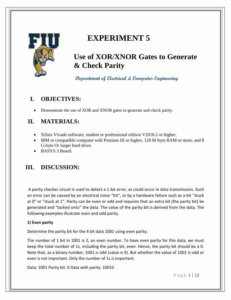
1. Open Xilinix Vivado and in the Xilinx-Project Navigator window, Quick start,
New Project.
2. Choose “RTL Project” and check the “Do not specify sources at this time” as we will
configure all the settings manually through the navigator from inside the project.
P a g e 3 | 12
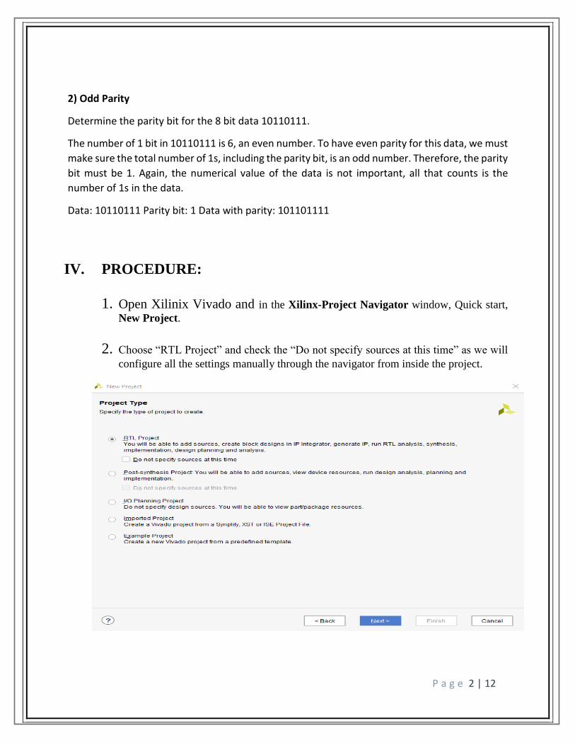
3. Select New Source… and the New window appears. In the New window, choose
Schematic, type your file name (such as eparity) in the File Name editor box, click on
OK, and then click on the Next button.
4. In the Xilinx - Project Navigator window, select the following
Category: “General Purpose”
Family: “Artix-7”
Package: “cpg236”
Speed: “-1”
Choose “xc7a35tcpg236-1” that corresponds to the board we are using.
Then Choose Finish.
P a g e 4 | 12
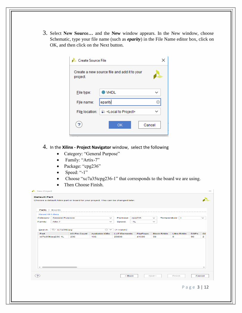
5. The Define Module Window that will appear, we will choose the input and output
labels for the gates under investigation in this experiment. In this experiment, we have
a bit victor as an input data. Then Under “Port Name”, add “clk” as input and then add
“Data_Tx” and “Data_Rx” then check the “Bus” and make the “MSB” equal to 7 as
we are designing an 8-bit parity check. Then, add “Parity”, as in/output as it will be
output from the transmitter stage then input to the Rx stage. Alsi, add “Error” as output
and select OK.
6. In the “eparity.vhd” created file, type the gates equivalent VHDL code for the 8-bit
even parity transmitter/ receiver between the “begin” and “end Behavioral” as follows
and then save the file.
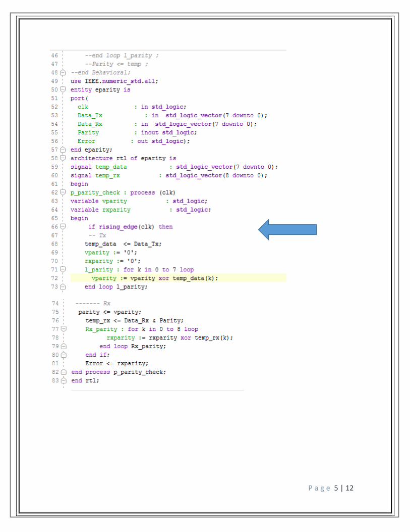
P a g e 5 | 12

P a g e 6 | 12
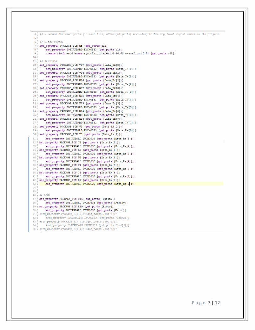
7. Next, we need to add To add a constraint file with the”.xdc” extension, as following:
Go to “Flow Navigator” and from “Project Manager” select “Add Sources” then “Add
or create constraints”. Next, choose “Create File” and enter the file name “lab_2” then
“OK” followed by “Finish”.
8. Then, we need to get a template xdc file that is going to be edited according to the
different experiments. Google “basys 3 xdc file” and choose the “xilinix” link that
appears (https://www.xilinx.com/support/documentation/university/Vivado-
Teaching/HDL-Design/2015x/Basys3/Supporting%20Material/Basys3_Master.xdc).
Copy the whole file and paste it into the “port_assign.xdc” that you have just created
in the last step. Then uncomment and edit the input Switches and the output LEDs as
in the next step.
P a g e 7 | 12
P a g e 8 | 12
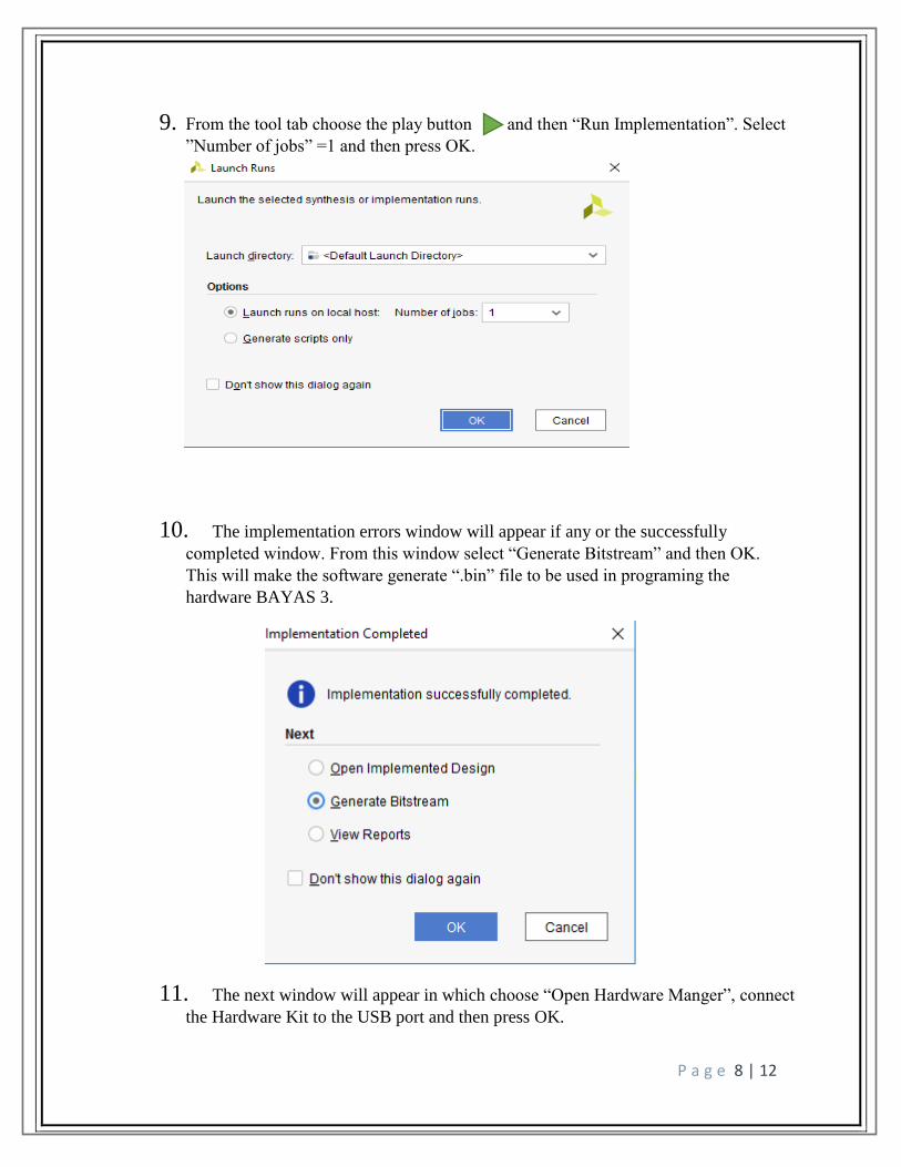
9. From the tool tab choose the play button and then “Run Implementation”. Select
”Number of jobs” =1 and then press OK.
10. The implementation errors window will appear if any or the successfully
completed window. From this window select “Generate Bitstream” and then OK.
This will make the software generate “.bin” file to be used in programing the
hardware BAYAS 3.
11. The next window will appear in which choose “Open Hardware Manger”, connect
the Hardware Kit to the USB port and then press OK.
P a g e 9 | 12
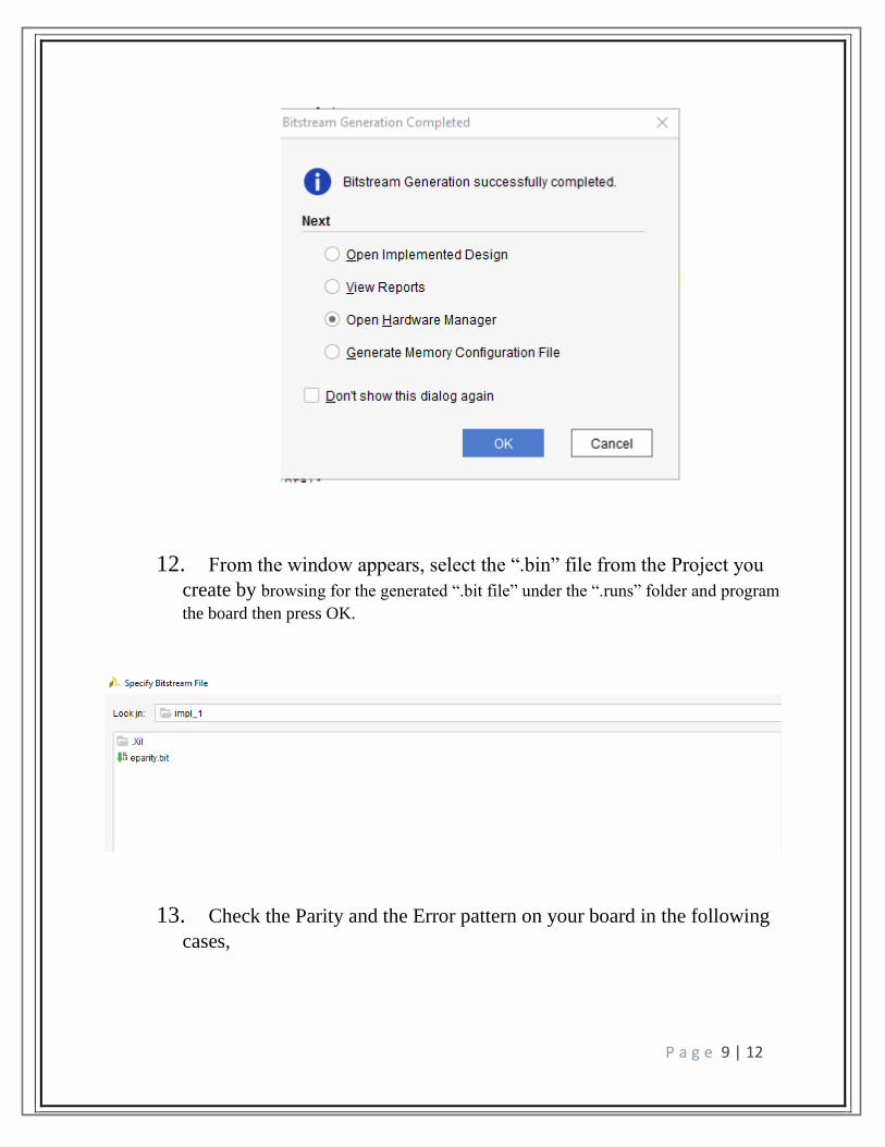
12. From the window appears, select the “.bin” file from the Project you
create by browsing for the generated “.bit file” under the “.runs” folder and program
the board then press OK.
13. Check the Parity and the Error pattern on your board in the following
cases,
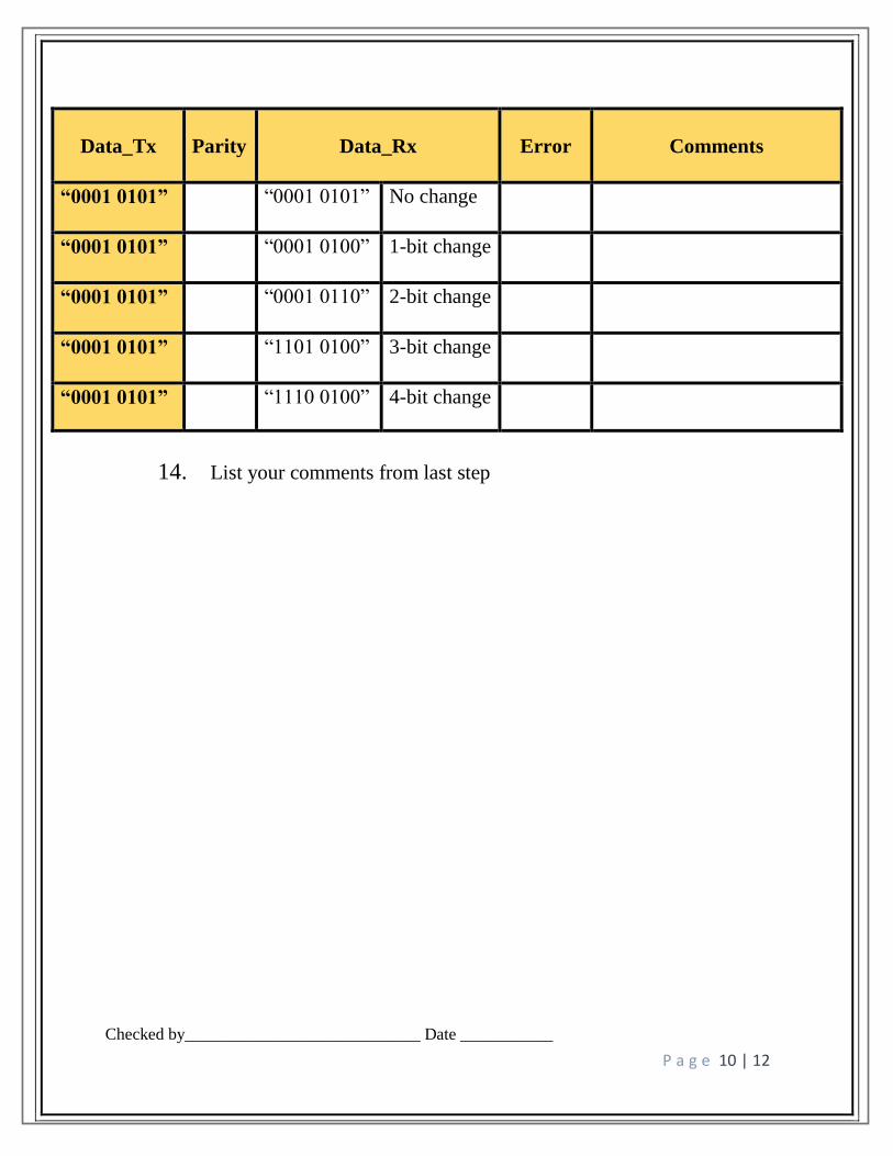
P a g e 10 | 12
Data_Tx
Parity
Data_Rx
Error
Comments
“0001 0101” “0001 0101” No change
“0001 0101” “0001 0100” 1-bit change
“0001 0101” “0001 0110” 2-bit change
“0001 0101” “1101 0100” 3-bit change
“0001 0101” “1110 0100” 4-bit change
14. List your comments from last step
Checked by____________________________ Date ___________
P a g e 11 | 12
V. Questions:
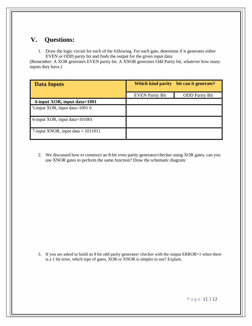
1. Draw the logic circuit for each of the following. For each gate, determine if it generates either
EVEN or ODD parity bit and finds the output for the given input data:
(Remember: A XOR generates EVEN parity bit. A XNOR generates Odd Parity bit, whatever how many
inputs they have.)
Data Inputs
Which kind parity
bit can it generate?
EVEN Parity Bit ODD Parity Bit
4-input XOR, input data=1001
5-input XOR, input data=1001 0
6-input XOR, input data=101001
7-input XNOR, input data = 1011011
2. We discussed how to construct an 8-bit even parity generator/checker using XOR gates, can you
use XNOR gates to perform the same function? Draw the schematic diagram.
3. If you are asked to build an 8 bit odd parity generator/ checker with the output ERROR=1 when there
is a 1 bit error, which type of gates, XOR or XNOR is simpler to use? Explain.

P a g e 12 | 12
4. Why can’t a parity generator/checker detect even-bit errors? Given an example in your explanation.


![Quantitative Transformation for Implementation of … · Quantitative Transformation for Implementation of Adder Circuits in ... NAND , XOR and XNOR [34], indi-4 ... The full adder](https://static.fdocuments.in/doc/165x107/5b68099f7f8b9a20388c1fb7/quantitative-transformation-for-implementation-of-quantitative-transformation.jpg)