Understanding and Comparisons of High Speed … and Comparisons of High Speed ADC and DAC...
17
Understanding and Comparisons of High Speed ADC and DAC Architectures TIPL 4706 Presented by Richard Prentice Prepared by Richard Prentice 1
-
Upload
nguyenmien -
Category
Documents
-
view
223 -
download
1
Transcript of Understanding and Comparisons of High Speed … and Comparisons of High Speed ADC and DAC...

Understanding and Comparisons of High Speed ADC and DAC Architectures TIPL 4706
Presented by Richard PrenticePrepared by Richard Prentice
1

Architectures
• Flash converter– Track and hold
• Comparators– For n bits:
• 2n – 1 comparators-
AnalogInput
1K
3K
1K
1K
1K
1K
1K
1K
VDD
-
+
-
+
-
+
-
+
-
+
+
-
+1
2
3
4
5
6
7
ENCO
DER
LOG
IC
Comparators
MSB
DigitalOutput
LSB

Architectures• Pipelined – successive stages of flash
– Each stage adds n bits more precision• Requires good matching/trimming
X X X X X 0 0 0 0 0 0 0 0 0
0 0 0 0 X X X X X 0 0 0 0 0
0 0 0 0 0 0 0 0 X X X X X X

Architectures• SAR – Successive Approximation
– DAC = digital-to-analog converter– EOC = end of conversion– SAR = successive approximation register– S/H = sample and hold circuit– Vin = input voltage– Vref = reference voltage
• Source - Wikipedia
4
SuccessiveApproximation
Register
DAC
S/H
-+
ClockEnd of
Conversion
VREF
VIN
Comparator
DN-1 DN-2 D0D1D2
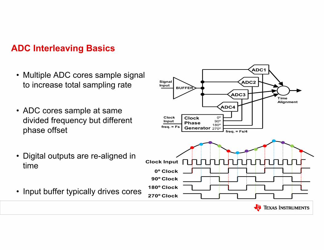
• Multiple ADC cores sample signal to increase total sampling rate
• ADC cores sample at same divided frequency but different phase offset
• Digital outputs are re-aligned in time
• Input buffer typically drives cores
Clock Input
0º Clock90º Clock
180º Clock
270º Clock
ADC1
ADC2
ADC3
ADC4
BUFFER
Signal Input
0º90º
180º270º
Clock PhaseGenerator
Clock Input
freq. = Fsfreq. = Fs/4
TimeAlignment
ADC Interleaving Basics
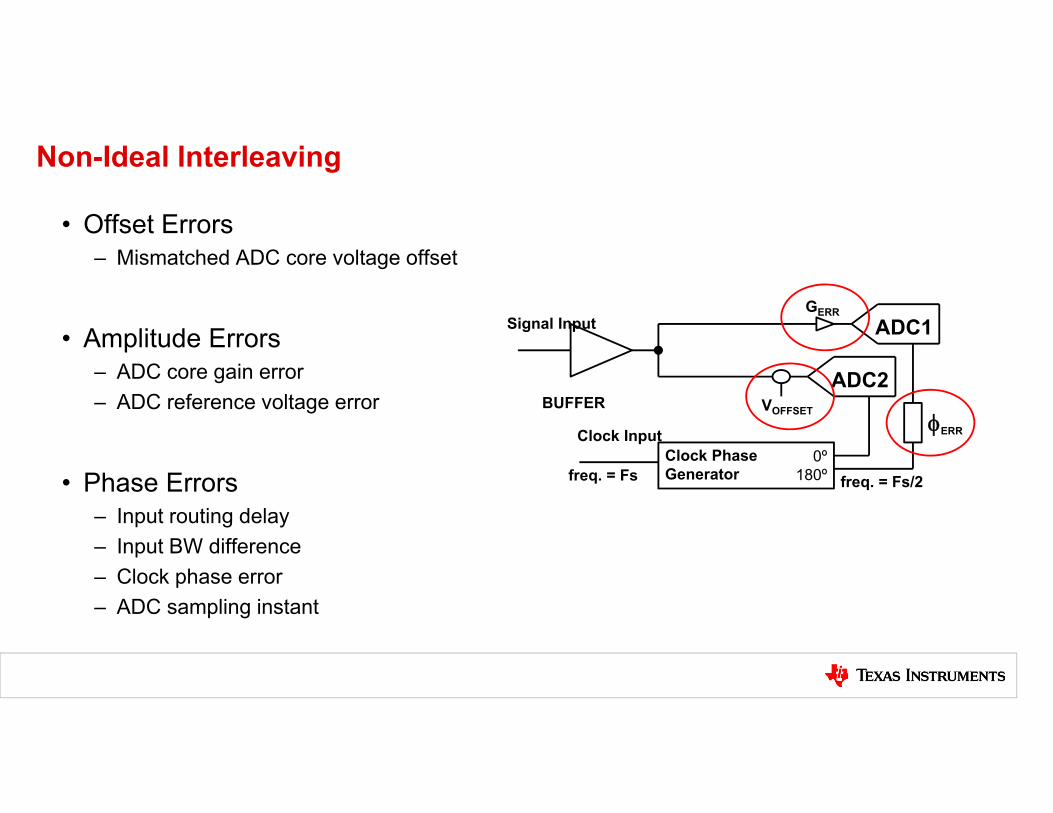
• Offset Errors– Mismatched ADC core voltage offset
• Amplitude Errors– ADC core gain error– ADC reference voltage error
• Phase Errors– Input routing delay– Input BW difference– Clock phase error– ADC sampling instant
ADC1
ADC2BUFFER
Signal Input
0º180º
Clock PhaseGenerator
Clock Input
freq. = Fs freq. = Fs/2
GERR
VOFFSETERR
Non-Ideal Interleaving
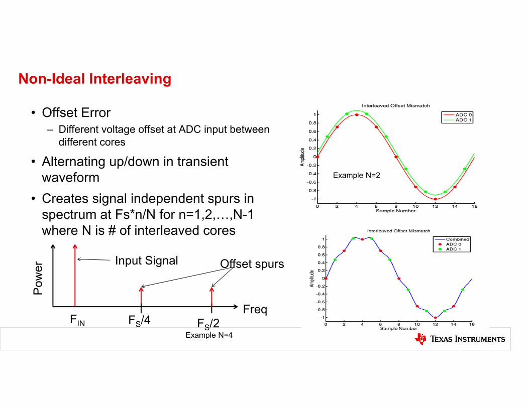
• Offset Error– Different voltage offset at ADC input between
different cores
• Alternating up/down in transient waveform
• Creates signal independent spurs in spectrum at Fs*n/N for n=1,2,…,N-1 where N is # of interleaved cores
FS/2Freq
FIN
Input Signal Offset spurs
Pow
er
Example N=4
FS/4
Example N=2
Non-Ideal Interleaving

• Amplitude (Gain) errors– Gain difference between different ADC cores
• Creates N-1 input signal dependent images from 0 to Fs/2 in a repetitive, mirror-image pattern where N is # of interleaved cores
• Also creates harmonic distortion images
FS/2Freq
FIN
Input Signal
Input Images
Pow
er
Example N=4FS/4
H2H2 Images
Non-Ideal Interleaving

• Relying on process matching not suitable for most applications• Interleave correction reduces spectrum offset spurs and images• Estimate the errors and correct the data with coefficients• Estimation
– Detection in time-domain or frequency domain– Convergence
• Correction– Analog/Digital
• Calibration time– Foreground: Calibration interrupts normal operation– Background: Calibration runs continuously
Interleaving Correction

Current Steering DAC
10
Dec
oder
Logi
c
Dig
ital I
nput
D
ata
Switc
h D
river
s
CurrentSource Array
BiasCircuit
IOUT1
Switch Array
IOUT2 Anal
og
Out
put
DAC =
30mA0mA
15mA15mA
0mA30mA
IOUT2IOUT1Full Scale = 30mA

DACs can be current source or current sink
11
+1/0.5 Volts
- 1/0.5 Volts IoutIoutb
VCC IoutIoutb
DAC90x, DAC290x, DAC2932, DAC56x2
DAC34xx, DAC3174
DAC5686/87/88/89, DAC5681/82Z,DAC3282/83DAC3152/62
PMOS NMOSC
urre
nt S
ourc
e C
asco
des
Switc
hes
Switc
hes
Cur
rent
Sin
k C
asco
des
VCC+ 0.5 Volts
VCC - 0.5 Volts

Simple 3-bit Binary DAC
12
bit 301
500uA
bit 201
250uA
bit 11
125uA
0
Vout
Vout
000 001 010 011 100 101 110 111
– (875u*1K)– (625u*1K)
(875u*1K)
– (375u*1K)– (125u*1K)
(125u*1K)(375u*1K)
(625u*1K)
bit 3bit 2bit 1
bit1 and bit2 turn off, bit3 turns on
10001000
AVDD AVDDPro: Least number of current sources and switches.Con: Higher distortion.

Equivalent 3-bit Thermometer Coded DAC
13
therm 11
125uA
0
Vout
bit 3bit 2bit 1
Vout
0000000
– (875u*1K)– (625u*1K)
(875u*1K)
– (375u*1K)– (125u*1K)
(125u*1K)(375u*1K)
(625u*1K)
therm 21
125uA
therm 71
125uA
00
0000001 0000011 0000111 0001111 0011111 0111111 1111111one more equal valued current source turns on
10001000
AVDD AVDDPro: Reduced distortion (easier to match equal current sources.)Con: More current sources and switches required.

DACs can be segmented and mixed coded
14
therm 11
125uA
0
Vout
10001000
AVDD AVDD
therm 21
125uA
therm 71
125uA
00
bit 301
62.5uA
bit 201
31.25uA
bit 11
15.625uA
0Binary 3b LSB DAC
Thermometer 3b MSB DAC
therm(7:1) to MSB segmentbit(3:1) to LSB segment
input 6b word decoder logic

Simplified TI 16b DAC topology
15
MSB segment decoding
LSB segment decoding
D(15:10)
D(9:0)
MSB Thermo(63:0)
LSB binary(9:0)
73 switch drivers
MSB current sources
LSB current sources
MSB cascodes
LSB cascodes
bias circuits
IOUT1
EXTIO
RBIAS
63 10
73 switches(6 MSB Bits)
(10 LSB Bits)
IOUT2
Ex: DAC34xx

Thanks for your time!
16

© Copyright 2017 Texas Instruments Incorporated. All rights reserved.This material is provided strictly “as-is,” for informational purposes only, and without any warranty.
Use of this material is subject to TI’s , viewable at TI.com