Ultra Low Power Stereo Audio Codec With Integrated ...
36
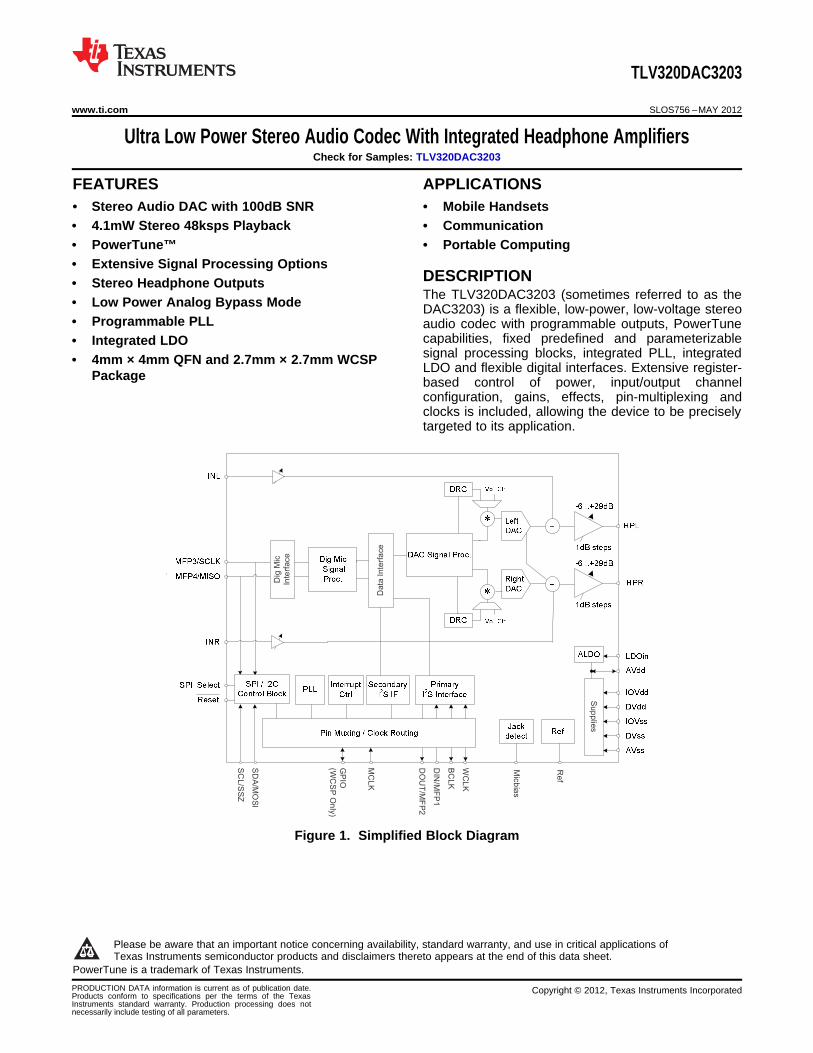
Micbias Supplies SCL/SSZ SDA/MOSI MCLK DOUT/MFP2 DIN/MFP1 BCLK WCLK GPIO (WCSP Only) Ref Data Interface Dig Mic Interface TLV320DAC3203 www.ti.com SLOS756 – MAY 2012 Ultra Low Power Stereo Audio Codec With Integrated Headphone Amplifiers Check for Samples: TLV320DAC3203 1FEATURES APPLICATIONS 2• Stereo Audio DAC with 100dB SNR • Mobile Handsets • 4.1mW Stereo 48ksps Playback • Communication • PowerTune™ • Portable Computing • Extensive Signal Processing Options DESCRIPTION • Stereo Headphone Outputs The TLV320DAC3203 (sometimes referred to as the • Low Power Analog Bypass Mode DAC3203) is a flexible, low-power, low-voltage stereo • Programmable PLL audio codec with programmable outputs, PowerTune capabilities, fixed predefined and parameterizable • Integrated LDO signal processing blocks, integrated PLL, integrated • 4mm × 4mm QFN and 2.7mm × 2.7mm WCSP LDO and flexible digital interfaces. Extensive register- Package based control of power, input/output channel configuration, gains, effects, pin-multiplexing and clocks is included, allowing the device to be precisely targeted to its application. Figure 1. Simplified Block Diagram 1 Please be aware that an important notice concerning availability, standard warranty, and use in critical applications of Texas Instruments semiconductor products and disclaimers thereto appears at the end of this data sheet. 2PowerTune is a trademark of Texas Instruments. PRODUCTION DATA information is current as of publication date. Copyright © 2012, Texas Instruments Incorporated Products conform to specifications per the terms of the Texas Instruments standard warranty. Production processing does not necessarily include testing of all parameters.
Transcript of Ultra Low Power Stereo Audio Codec With Integrated ...
Mic
bia
s
Sup
plie
s
SC
L/S
SZ
SD
A/M
OS
I
MC
LK
DO
UT
/MF
P2
DIN
/MF
P1
BC
LK
WC
LK
GP
IO
(WC
SP
On
ly)
Ref
Data
Inte
rfa
ce
Dig
Mic
Inte
rface
TLV320DAC3203
www.ti.com SLOS756 –MAY 2012
Ultra Low Power Stereo Audio Codec With Integrated Headphone AmplifiersCheck for Samples: TLV320DAC3203
1FEATURES APPLICATIONS2• Stereo Audio DAC with 100dB SNR • Mobile Handsets• 4.1mW Stereo 48ksps Playback • Communication• PowerTune™ • Portable Computing• Extensive Signal Processing Options
DESCRIPTION• Stereo Headphone OutputsThe TLV320DAC3203 (sometimes referred to as the• Low Power Analog Bypass Mode DAC3203) is a flexible, low-power, low-voltage stereo
• Programmable PLL audio codec with programmable outputs, PowerTunecapabilities, fixed predefined and parameterizable• Integrated LDOsignal processing blocks, integrated PLL, integrated• 4mm × 4mm QFN and 2.7mm × 2.7mm WCSPLDO and flexible digital interfaces. Extensive register-
Package based control of power, input/output channelconfiguration, gains, effects, pin-multiplexing andclocks is included, allowing the device to be preciselytargeted to its application.
Figure 1. Simplified Block Diagram
1
Please be aware that an important notice concerning availability, standard warranty, and use in critical applications ofTexas Instruments semiconductor products and disclaimers thereto appears at the end of this data sheet.
2PowerTune is a trademark of Texas Instruments.
PRODUCTION DATA information is current as of publication date. Copyright © 2012, Texas Instruments IncorporatedProducts conform to specifications per the terms of the TexasInstruments standard warranty. Production processing does notnecessarily include testing of all parameters.

TLV320DAC3203
SLOS756 –MAY 2012 www.ti.com
This integrated circuit can be damaged by ESD. Texas Instruments recommends that all integrated circuits be handled withappropriate precautions. Failure to observe proper handling and installation procedures can cause damage.
ESD damage can range from subtle performance degradation to complete device failure. Precision integrated circuits may be moresusceptible to damage because very small parametric changes could cause the device not to meet its published specifications.
DESCRIPTION (CONTINUED)Combined with the advanced PowerTune technology, the device can cover operations from 8kHz mono voiceplayback to stereo 192kHz DAC playback, making it ideal for portable battery-powered audio and telephonyapplications.
The playback path offers signal processing blocks for filtering and effects, true differential output signal, flexiblemixing of DAC and analog input signals as well as programmable volume controls. The TLV320DAC3203contains two high-power output drivers which can be configured in multiple ways, including stereo and monoBTL. The integrated PowerTune technology allows the device to be tuned to just the right power-performancetrade-off. Mobile applications frequently have multiple use cases requiring very low-power operation while beingused in a mobile environment. When used in a docked environment, power consumption typically is less of aconcern and lowest possible noise is more important. With PowerTune the TLV320DAC3203 can address bothcases.
The voltage supply range for the TLV320DAC3203 for analog is 1.5V–1.95V, and for digital it is 1.26V–1.95V. Toease system-level design, a low-dropout regulator (LDO) is integrated to generate the appropriate analog supplyfrom input voltages ranging from 1.8V to 3.6V. Digital I/O voltages are supported in the range of 1.1V–3.6V.
The required internal clock of the TLV320DAC3203 can be derived from multiple sources, including the MCLK,BCLK, GPIO pins or the output of internal PLL, where the input to the PLL again can be derived from the MCLK,BCLK or GPIO pins. Although using the internal, fractional PLL ensures the availability of a suitable clock signal,it is not recommended for the lowest power settings. The PLL is highly programmable and can accept availableinput clocks in the range of 512kHz to 50MHz.
The device is available in the 4mm × 4mm QFN and 2.7mm × 2.7mm WCSP package.
2 Copyright © 2012, Texas Instruments Incorporated
DVss
DVdd
IOVdd (24)
SDA/MOSI
DMCLK/MFP4
NC
LDOin
NC
DO
UT
/MF
P2
DIN
/MF
P1
WC
LK
BC
LK
MC
LK
(1)
MIC
BIA
S
NC
NC
NC
AV
ss
AV
dd
DM
DIN
/MF
P3
SCL/SS
RESET
SPI_SELECT
IOVss
B
C
D
E
A
1 2 3 4 5
TLV320DAC3203
www.ti.com SLOS756 –MAY 2012
Package and Signal Descriptions
Packaging/Ordering Information
PRODUCT PACKAGE PACKAGE OPERATING ORDERING TRANSPORT MEDIA,DESIGNATOR TEMPERATURE NUMBER QUANTITY
RANGE
S-XBGA-N25 YZK –40°C to 85°C TLV320DAC3203IYZKT Tape and Reel, 250
TLV320DAC3203IYZKR Tape and Reel, 3000TLV320DAC3203
S-PVQFN-N24 RGE –40°C to 85°C TLV320DAC3203IRGET Tape and Reel, 250
TLV320DAC3203IRGER Tape and Reel, 3000
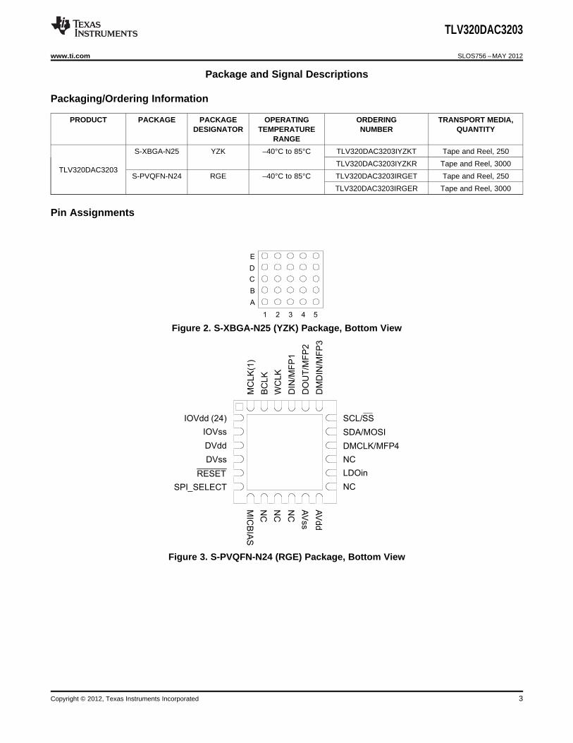
Pin Assignments
spacespace
Figure 2. S-XBGA-N25 (YZK) Package, Bottom View
Figure 3. S-PVQFN-N24 (RGE) Package, Bottom View
Copyright © 2012, Texas Instruments Incorporated 3

TLV320DAC3203
SLOS756 –MAY 2012 www.ti.com
TERMINAL FUNCTIONSTERMINAL
NAME TYPE DESCRIPTION (1) (2)QFN PIN WCSP
BALL
1 A1 MCLK I Master Clock Input
2 B2 BCLK IO Audio serial data bus (primary) bit clock
3 B3 WCLK IO Audio serial data bus (primary) word clock
4 A2 DIN/MFP1 I Primary function
Audio serial data bus data input
Secondary function
Digital Microphone InputGeneral Purpose Input
5 A3 DOUT/MFP2 O Primary
Audio serial data bus data output
Secondary
General Purpose OutputClock OutputINT1 OutputINT2 OutputAudio serial data bus (secondary) bit clock outputAudio serial data bus (secondary) word clock output
6 A5 DMDIN/ I Primary (SPI_Select = 1)MFP3/ SPI serial clockSCLK
Secondary: (SPI_Select = 0)
Digital microphone inputHeadset detect inputAudio serial data bus (secondary) bit clock inputAudio serial data bus (secondary) DAC/common word clock inputAudio serial data bus (secondary) ADC word clock inputAudio serial data bus (secondary) data inputGeneral Purpose Input
7 A4 SCL/ I I2C interface serial clock (SPI_Select = 0)SS SPI interface mode chip-select signal (SPI_Select = 1)
8 B4 SDA/ MOSI I I2C interface mode serial data input (SPI_Select = 0)SPI interface mode serial data input (SPI_Select = 1)
9 B5 DMCLK/ O Primary (SPI_Select = 1)MFP4/ Serial data outputMISO
Secondary (SPI_Select = 0) Multifunction pin #4 (MFP4) options are only availableusing I2C
Digital microphone clock outputGeneral purpose outputCLKOUT outputINT1 outputINT2 outputAudio serial data bus (primary) ADC word clock outputAudio serial data bus (secondary) data outputAudio serial data bus (secondary) bit clock outputAudio serial data bus (secondary) word clock output
10 C5 HPR O Right high-power output driver
11 D5 LDOIN/ Power LDO Input supply and Headphone Power supply 1.9V– 3.6VHPVDD
12 D4 HPL O Left high power output driver
(1) For multiple BGA Balls assigned to the same pin-name, it is necessary to connect them on the PCB.(2) For multiple BGA Balls assigned to the same pin-name, it is recommended to connect them on the PCB.
4 Copyright © 2012, Texas Instruments Incorporated

TLV320DAC3203
www.ti.com SLOS756 –MAY 2012
TERMINAL FUNCTIONS (continued)
TERMINALNAME TYPE DESCRIPTION (1) (2)
QFN PIN WCSPBALL
13 D3 AVDD Power Analog voltage supply 1.5V–1.95VInput when A-LDO disabled,Filtering output when A-LDO enabled
14 E4 AVSS Ground Analog ground supply
15 E5 INL I Left Analog Bypass Input
16 E3 INR I Right Analog Bypass Input
17 E2 REF O Reference voltage output for filtering
18 D2 MICBIAS O Microphone bias voltage output
19 E1 SPI_ SELECT I Control mode select pin ( 1 = SPI, 0 = I2C )
20 C2 RESET I Reset (active low)
21 D1 DVSS Ground Digital Ground and Chip-substrate
22 C1 DVDD Power Digital voltage supply 1.26V–1.95V
23 B1 IOVSS Ground I/O ground supply
24 C3 IOVDD Power I/O voltage supply 1.1V – 3.6V
n/a C4 GPIO/MFP5 I Primary
General Purpose digital IO
Secondary
CLKOUT OutputINT1 OutputINT2 OutputAudio serial data bus ADC word clock outputAudio serial data bus (secondary) bit clock outputAudio serial data bus (secondary) word clock outputDigital microphone clock output
Copyright © 2012, Texas Instruments Incorporated 5
TLV320DAC3203
SLOS756 –MAY 2012 www.ti.com
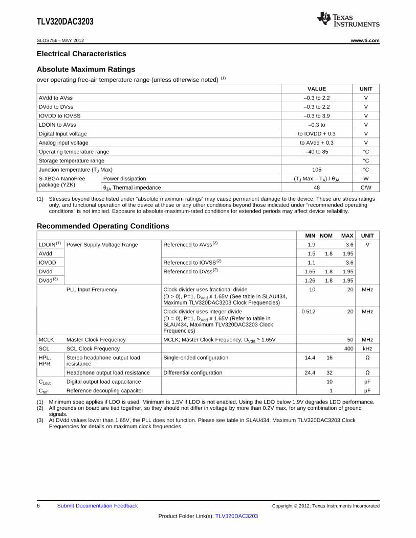
Electrical Characteristics
Absolute Maximum Ratingsover operating free-air temperature range (unless otherwise noted) (1)
VALUE UNIT
AVdd to AVss –0.3 to 2.2 V
DVdd to DVss –0.3 to 2.2 V
IOVDD to IOVSS –0.3 to 3.9 V
LDOIN to AVss –0.3 to V
Digital Input voltage to IOVDD + 0.3 V
Analog input voltage to AVdd + 0.3 V
Operating temperature range –40 to 85 °C
Storage temperature range °C
Junction temperature (TJ Max) 105 °C
S-XBGA NanoFree Power dissipation (TJ Max – TA) / θJA Wpackage (YZK) θJA Thermal impedance 48 C/W
(1) Stresses beyond those listed under “absolute maximum ratings” may cause permanent damage to the device. These are stress ratingsonly, and functional operation of the device at these or any other conditions beyond those indicated under “recommended operatingconditions” is not implied. Exposure to absolute-maximum-rated conditions for extended periods may affect device reliability.
Recommended Operating ConditionsMIN NOM MAX UNIT
LDOIN (1) Power Supply Voltage Range Referenced to AVss (2) 1.9 3.6 V
AVdd 1.5 1.8 1.95
IOVDD Referenced to IOVSS (2) 1.1 3.6
DVdd Referenced to DVss (2) 1.65 1.8 1.95
DVdd (3) 1.26 1.8 1.95
PLL Input Frequency Clock divider uses fractional divide 10 20 MHz(D > 0), P=1, DVdd ≥ 1.65V (See table in SLAU434,Maximum TLV320DAC3203 Clock Frequencies)
Clock divider uses integer divide 0.512 20 MHz(D = 0), P=1, DVdd ≥ 1.65V (Refer to table inSLAU434, Maximum TLV320DAC3203 ClockFrequencies)
MCLK Master Clock Frequency MCLK; Master Clock Frequency; DVdd ≥ 1.65V 50 MHz
SCL SCL Clock Frequency 400 kHz
HPL, Stereo headphone output load Single-ended configuration 14.4 16 ΩHPR resistance
Headphone output load resistance Differential configuration 24.4 32 ΩCLout Digital output load capacitance 10 pF
Cref Reference decoupling capacitor 1 µF
(1) Minimum spec applies if LDO is used. Minimum is 1.5V if LDO is not enabled. Using the LDO below 1.9V degrades LDO performance.(2) All grounds on board are tied together, so they should not differ in voltage by more than 0.2V max, for any combination of ground
signals.(3) At DVdd values lower than 1.65V, the PLL does not function. Please see table in SLAU434, Maximum TLV320DAC3203 Clock
Frequencies for details on maximum clock frequencies.
6 Submit Documentation Feedback Copyright © 2012, Texas Instruments Incorporated
Product Folder Link(s): TLV320DAC3203

TLV320DAC3203
www.ti.com SLOS756 –MAY 2012
Electrical Characteristics, Bypass OutputsAt 25°C, AVdd, DVdd, IOVDD = 1.8V, LDO_in = 1.8V, AVdd LDO disabled, fs (Audio) = 48kHz, Cref = 10μF on REF PIN, PLLdisabled unless otherwise noted.
PARAMETER TEST CONDITIONS MIN TYP MAX UNIT
ANALOG BYPASS TO HEADPHONE AMPLIFIER, DIRECT MODE
Load = 16Ω (single-ended), 50pF;Input and Output CM = 0.9V;
Device Setup Headphone Output on LDOIN Supply;INL routed to HPL and INR routed to HPR;Channel Gain = 0dB
Gain Error ±0.4 dB
Noise, A-weighted (1) Idle Channel, INL and INR ac-shorted to 3 μVRMSground
THD Total Harmonic Distortion 446mVrms, 1-kHz input signal –82 dB
(1) All performance measurements done with 20-kHz low-pass filter and, where noted, A-weighted filter. Failure to use such a filter mayresult in higher THD+N and lower SNR and dynamic range readings than shown in the Electrical Characteristics. The low-pass filterremoves out-of-band noise, which, although not audible, may affect dynamic specification values
Electrical Characteristics, Microphone InterfaceAt 25°C, AVdd, DVdd, IOVDD = 1.8V, LDO_in = 1.8V, AVdd LDO disabled, Cref = 10μF on REF PIN, PLL disabled unlessotherwise noted.
PARAMETER TEST CONDITIONS MIN TYP MAX UNIT
MICROPHONE BIAS
Bias voltage Bias voltage CM=0.9V, LDOin = 3.3V, no load
Micbias Mode 0, Connect to AVdd or LDOin 1.25 V
Micbias Mode 1, Connect to LDOin 1.7 V
Micbias Mode 2, Connect to LDOin 2.5 V
Micbias Mode 3, Connect to AVdd AVdd V
Micbias Mode 3, Connect to LDOin LDOin V
CM = 0.75V, LDOin = 3.3V
Micbias Mode 0, Connect to AVdd or LDOin 1.04 V
Micbias Mode 1, Connect to AVdd or LDOin 1.42 V
Micbias Mode 2, Connect to LDOin 2.08 V
Micbias Mode 3, Connect to AVdd AVdd V
Micbias Mode 3, Connect to LDOin LDOin V
Output Noise CM = 0.9V, Micbias Mode 2, A-weighted, 1020Hz to 20kHz bandwidth, μVRMSCurrent load = 0mA.
Current Sourcing Micbias Mode 2, Connect to LDOin 3 mA
Micbias Mode 3, Connect to AVdd 160Inline Resistance Ω
Micbias Mode 3, Connect to LDOin 110
Copyright © 2012, Texas Instruments Incorporated Submit Documentation Feedback 7
Product Folder Link(s): TLV320DAC3203

TLV320DAC3203
SLOS756 –MAY 2012 www.ti.com
Electrical Characteristics, Audio OutputsAt 25°C, AVdd, DVdd, IOVDD = 1.8V, LDO_in = 1.8V, AVdd LDO disabled, fs (Audio) = 48kHz, Cref = 10 μF on REF PIN,PLL disabled unless otherwise noted.
PARAMETER TEST CONDITIONS MIN TYP MAX UNIT
Audio DAC – Stereo Single-Ended Headphone Output
Load = 16Ω (single-ended), 50pFHeadphone Output on AVdd Supply,Input & Output CM = 0.9V, DOSR = 128,
Device Setup MCLK = 256* fs, Channel Gain = 0dBword length = 16 bits;Processing Block = PRB_P1Power Tune = PTM_P3
Full scale output voltage (0dB) 0.5 VRMS
SNR Signal-to-noise ratio, A-weighted (1) (2) All zeros fed to DAC input, modulator in 88 100 dBexcited state
DR Dynamic range, A-weighted (1) (2) –60dB 1kHz input full-scale signal, Word 99 dBLength = 20 bits, Power Tune = PTM_P4
THD+N Total Harmonic Distortion plus Noise –3dB full-scale, 1-kHz input signal –80 –70 dB
DAC Gain Error 0dB, 1kHz input full scale signal ±0.1 dB
DAC Mute Attenuation Mute 127 dB
DAC channel separation –1dB, 1kHz signal, between left and right HP 92 dBout
100mVpp, 1kHz signal applied to AVdd 70 dBDAC PSRR
100mVpp, 217Hz signal applied to AVdd 75 dB
RL=16Ω, Output Stage on AVdd = 1.8V 13THDN < 1%, Input CM=0.9V,Output CM=0.9V, Channel Gain = 2dB
Power Delivered mWRL= 16Ω Output Stage on LDOIN = 3.3V, 47THDN < 1% Input CM = 0.9V,Output CM = 1.65V, Channel Gain = 8dB
Audio DAC – Stereo Single-Ended Headphone Output
Load = 16Ω (single-ended), 50pF,Headphone Output on AVdd Supply,Input & Output CM = 0.75V; AVdd = 1.5V,
Device Setup DOSR = 128, MCLK = 256* fs,Channel Gain = –2dB, word length = 20-bits;Processing Block = PRB_P1,Power Tune = PTM_P4
Full scale output voltage (0dB) 0.375 VRMS
SNR Signal-to-noise ratio, A-weighted (1) (2) All zeros fed to DAC input, modulator in 99 dBexcited state
DR Dynamic range, A-weighted (1) (2) -60dB 1 kHz input full-scale signal 98 dB
THD+N Total Harmonic Distortion plus Noise –3dB full-scale, 1-kHz input signal –84 dB
Audio DAC – Mono Differential Headphone Output
Load = 32 Ω (differential), 50pF,Headphone Output on LDOIN SupplyInput CM = 0.75V, Output CM = 1.5V,AVdd=1.8V, LDOIN = 3.0V, DOSR = 128
Device Setup MCLK = 256* fs, Channel (headphone driver)Gain = 5dB for full scale output signal,word length = 16-bits,Processing Block = PRB_P1,Power Tune = PTM_P3
(1) Ratio of output level with 1-kHz full-scale sine wave input, to the output level with the inputs short circuited, measured A-weighted over a20-Hz to 20-kHz bandwidth using an audio analyzer.
(2) All performance measurements done with 20-kHz low-pass filter and, where noted, A-weighted filter. Failure to use such a filter mayresult in higher THD+N and lower SNR and dynamic range readings than shown in the Electrical Characteristics. The low-pass filterremoves out-of-band noise, which, although not audible, may affect dynamic specification values
8 Submit Documentation Feedback Copyright © 2012, Texas Instruments Incorporated
Product Folder Link(s): TLV320DAC3203

TLV320DAC3203
www.ti.com SLOS756 –MAY 2012
Electrical Characteristics, Audio Outputs (continued)At 25°C, AVdd, DVdd, IOVDD = 1.8V, LDO_in = 1.8V, AVdd LDO disabled, fs (Audio) = 48kHz, Cref = 10 μF on REF PIN,PLL disabled unless otherwise noted.
PARAMETER TEST CONDITIONS MIN TYP MAX UNIT
Full scale output voltage (0dB) 1778 mVRMS
SNR Signal-to-noise ratio, A-weighted (1) (2) All zeros fed to DAC input, modulator in 101 dBexcited state
DR Dynamic range, A-weighted (1) (2) –60dB 1kHz input full-scale signal 98 dB
THD Total Harmonic Distortion –3dB full-scale, 1-kHz input signal –82 dB
RL = 32Ω, Output Stage on LDOIN = 3.3V, 125 mWTHDN < 1%, Input CM = 0.9V,Output CM = 1.65V, Channel Gain = 8dB
Power DeliveredRL = 32Ω Output Stage on LDOIN = 3.0V, 103 mWTHDN < 1% Input CM = 0.9V,Output CM = 1.5V, Channel Gain = 8dB
Electrical Characteristics, LDOover operating free-air temperature range (unless otherwise noted)
PARAMETER TEST CONDITIONS MIN TYP MAX UNIT
LOW DROPOUT REGULATOR (AVdd)
LDOMode = 1, LDOin > 1.95V, 1.63IO = 15mA
LDOMode = 0, LDOin > 2.0V, 1.68Output Voltage VIO = 15mA
LDOMode = 2, LDOin > 2.05V, 1.73IO = 15mA
Output Voltage Accuracy ±2 %
Load Regulation Load current range 0 to 50mA 26 mV
Line Regulation Input Supply Range 1.9V to 3.6V 3 mV
Decoupling Capacitor 1 μF
Bias Current 50 μA
Electrical Characteristics, Misc.At 25°C, AVdd, DVdd, IOVDD = 1.8V, LDO_in = 3.3V, AVdd LDO disabled, fs (Audio) = 48kHz, Cref = 10 μF on REF PIN,PLL disabled unless otherwise noted.
PARAMETER TEST CONDITIONS MIN TYP MAX UNIT
REFERENCE
CMMode = 0 (0.9V) 0.9Reference Voltage Settings V
CMMode = 1 (0.75V) 0.75
Reference Noise CM=0.9V, A-weighted, 20Hz to 20kHz bandwidth, 1 μVRfcMSCref = 10μF
Decoupling Capacitor 1 10 μF
Bias Current 120 µA
Shutdown Current
Coarse AVdd supply turned off, LDO_select held atDevice Setup ground, No external digital input is toggled
IDVdd 1.4
IAVdd 1μA
ILDOin 1
IIOVDD <0.1
Copyright © 2012, Texas Instruments Incorporated Submit Documentation Feedback 9
Product Folder Link(s): TLV320DAC3203

TLV320DAC3203
SLOS756 –MAY 2012 www.ti.com
Electrical Characteristics, Logic LevelsAt 25°C, AVDD, DVDD, IOVDD = 1.8V
PARAMETER TEST CONDITIONS MIN TYP MAX UNIT
LOGIC FAMILY CMOS
VIH Logic Level IIH = 5 μA, IOVDD > 1.6V 0.7 × IOVDD V
IIH = 5μA, 1.2V ≤ IOVDD <1.6V 0.9 × IOVDD V
IIH = 5μA, IOVDD < 1.2V IOVDD V
VIL IIL = 5 μA, IOVDD > 1.6V –0.3 0.3 × IOVDD V
IIL = 5μA, 1.2V ≤ IOVDD <1.6V 0.1 × IOVDD V
IIL = 5μA, IOVDD < 1.2V 0 V
VOH IOH = 2 TTL loads 0.8 × IOVDD V
VOL IOL = 2 TTL loads 0.1 × IOVDD V
Capacitive Load 10 pF
10 Submit Documentation Feedback Copyright © 2012, Texas Instruments Incorporated
Product Folder Link(s): TLV320DAC3203

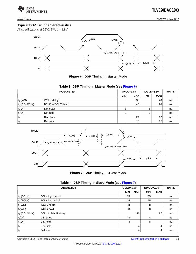
th(WS)
WCLK
BCLK
DOUT
DIN
tL(BCLK) tH(BCLK)
ts(WS)
td(DO-WS) td(DO-BCLK)
th(DI)ts(DI)
WCLK
BCLK
DOUT
DIN
t (WS)d
t (DO-WS)dt (DO-BCLK)d
t (DI)St (DI)h
I2S/LJF Timing in Master Mode
TLV320DAC3203
www.ti.com SLOS756 –MAY 2012
Interface Timing
Typical Timing Characteristics — Audio Data Serial Interface Timing (I2S)All specifications at 25°C, DVdd = 1.8V
Figure 4. I2S/LJF/RJF Timing in Master Mode
Table 1. I2S/LJF/RJF Timing in Master Mode (see Figure 4)
PARAMETER IOVDD=1.8V IOVDD=3.3V UNITS
MIN MAX MIN MAX
td(WS) WCLK delay 30 20 ns
td (DO-WS) WCLK to DOUT delay (For LJF Mode only) 50 25 ns
td (DO-BCLK) BCLK to DOUT delay 50 25 ns
ts(DI) DIN setup 8 8 ns
th(DI) DIN hold 8 8 ns
tr Rise time 24 12 ns
tf Fall time 24 15 ns
Figure 5. I2S/LJF/RJF Timing in Slave Mode
Copyright © 2012, Texas Instruments Incorporated Submit Documentation Feedback 11
Product Folder Link(s): TLV320DAC3203

TLV320DAC3203
SLOS756 –MAY 2012 www.ti.com
Table 2. I2S/LJF/RJF Timing in Slave Mode (see Figure 5)
PARAMETER IOVDD=1.8V IOVDD=3.3V UNITS
MIN MAX MIN MAX
tH (BCLK) BCLK high period 35 35 ns
tL (BCLK) BCLK low period 35 35
ts (WS) WCLK setup 8 8
th (WS) WCLK hold 8 8
td (DO-WS) WCLK to DOUT delay (For LJF mode only) 50 25
td (DO-BCLK) BCLK to DOUT delay 50 25
ts(DI) DIN setup 8 8
th(DI) DIN hold 8 8
tr Rise time 4 4
tf Fall time 4 4
12 Submit Documentation Feedback Copyright © 2012, Texas Instruments Incorporated
Product Folder Link(s): TLV320DAC3203
WCLK
BCLK
DOUT
DIN
t (BCLK)H
t (ws)h
t (BCLK)L
t (ws)st (ws)h
t (DO-BCLK)d
t (ws)h
t (DI)st (DI)h
WCLK
BCLK
DOUT
DIN
t (WS)d t (WS)d
t (DO-BCLK)d
t (DI)st (DI)h
TLV320DAC3203
www.ti.com SLOS756 –MAY 2012
Typical DSP Timing CharacteristicsAll specifications at 25°C, DVdd = 1.8V
Figure 6. DSP Timing in Master Mode
Table 3. DSP Timing in Master Mode (see Figure 6)
PARAMETER IOVDD=1.8V IOVDD=3.3V UNITS
MIN MAX MIN MAX
td (WS) WCLK delay 30 20 ns
td (DO-BCLK) BCLK to DOUT delay 40 20 ns
ts(DI) DIN setup 8 8 ns
th(DI) DIN hold 8 8 ns
tr Rise time 24 12 ns
tf Fall time 24 12 ns
Figure 7. DSP Timing in Slave Mode
Table 4. DSP Timing in Slave Mode (see Figure 7)
PARAMETER IOVDD=1.8V IOVDD=3.3V UNITS
MIN MAX MIN MAX
tH (BCLK) BCLK high period 35 35 ns
tL (BCLK) BCLK low period 35 35 ns
ts(WS) WCLK setup 8 8 ns
th(WS) WCLK hold 8 8 ns
td (DO-BCLK) BCLK to DOUT delay 40 22 ns
ts(DI) DIN setup 8 8 ns
th(DI) DIN hold 8 8 ns
tr Rise time 4 4 ns
tf Fall time 4 4 ns
Copyright © 2012, Texas Instruments Incorporated Submit Documentation Feedback 13
Product Folder Link(s): TLV320DAC3203
TLV320DAC3203
SLOS756 –MAY 2012 www.ti.com
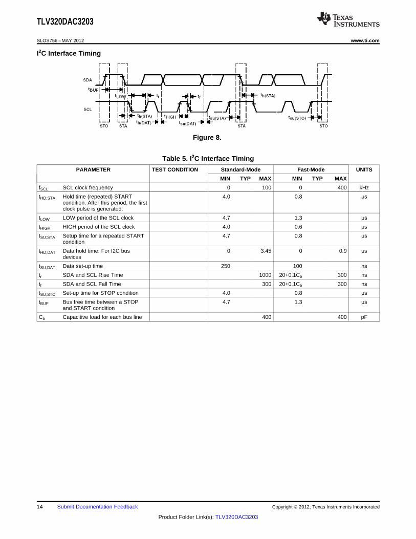
I2C Interface Timing
Figure 8.
Table 5. I2C Interface Timing
PARAMETER TEST CONDITION Standard-Mode Fast-Mode UNITS
MIN TYP MAX MIN TYP MAX
fSCL SCL clock frequency 0 100 0 400 kHz
tHD;STA Hold time (repeated) START 4.0 0.8 μscondition. After this period, the firstclock pulse is generated.
tLOW LOW period of the SCL clock 4.7 1.3 μs
tHIGH HIGH period of the SCL clock 4.0 0.6 μs
tSU;STA Setup time for a repeated START 4.7 0.8 μscondition
tHD;DAT Data hold time: For I2C bus 0 3.45 0 0.9 μsdevices
tSU;DAT Data set-up time 250 100 ns
tr SDA and SCL Rise Time 1000 20+0.1Cb 300 ns
tf SDA and SCL Fall Time 300 20+0.1Cb 300 ns
tSU;STO Set-up time for STOP condition 4.0 0.8 μs
tBUF Bus free time between a STOP 4.7 1.3 μsand START condition
Cb Capacitive load for each bus line 400 400 pF
14 Submit Documentation Feedback Copyright © 2012, Texas Instruments Incorporated
Product Folder Link(s): TLV320DAC3203

ttdS
ta
MSB OUT BIT 6 . . . 1 LSB OUT
tscktLead
tLag
tsckh
tsckl
trtf
tv tdis
MSB IN BIT 6 . . . 1 LSB IN
thitsu
SS
SCLK
MISO
MOSI
TLV320DAC3203
www.ti.com SLOS756 –MAY 2012
SPI Interface Timing
Figure 9. SPI Interface Timing Diagram
Timing Requirements (See Figure 9)At 25°C, DVdd = 1.8V
Table 6. SPI Interface Timing
PARAMETER TEST CONDITION IOVDD=1.8V IOVDD=3.3V UNITS
MIN TYP MAX MIN TYP MAX
tsck SCLK Period 100 50 ns
tsckh SCLK Pulse width High 50 25 ns
tsckl SCLK Pulse width Low 50 25 ns
tlead Enable Lead Time 30 20 ns
tlag Enable Lag Time 30 20 ns
td;seqxfr Sequential Transfer Delay 40 20 ns
ta Slave DOUT access time 40 20 ns
tdis Slave DOUT disable time 40 25 ns
tsu DIN data setup time 15 10 ns
th;DIN DIN data hold time 15 10 ns
tv;DOUT DOUT data valid time 45 25 ns
tr SCLK Rise Time 4 4 ns
tf SCLK Fall Time 4 4 ns
Copyright © 2012, Texas Instruments Incorporated Submit Documentation Feedback 15
Product Folder Link(s): TLV320DAC3203
60
65
70
75
80
85
90
95
100
105
0.75 0.9 1.25 1.5 1.65
Output Common Mode Setting - V
SN
R -
Sig
nal-
to-N
ois
e R
ati
o -
dB
0
10
20
30
40
50
60
70
SNR
SINGLE ENDED
OUTPUT POWER
16 , -40dB THDW
Ou
tpu
t P
ow
er
- m
W
0
50
100
150
200
250
0 10 20 30 40 50
Load - mA
Dro
po
ut
Vo
lta
ge
- m
V
-90
-80
-70
-60
-50
-40
-30
-20
-10
0
0 50 100 150 200
Headphone output Power - mW
TH
D -
To
tal H
arm
on
ic D
isto
rtio
n -
dB
Load = 32 BTLW
CM=1.5 V
CM=1.65 V
0 20 40 60 80 100
Headphone Output Power - mW
0
-10
-20
-30
-40
-50
-60
-70
-80
-90
TH
D -
To
tal H
arm
on
ic D
isto
rtio
n -
dB
CM=0.9 V,
R = 32L
W
CM=0.9 V,
R = 16L
W
CM=1.65 V,
R = 32L
W
CM=1.65 V,
R = 16L
W
TLV320DAC3203
SLOS756 –MAY 2012 www.ti.com
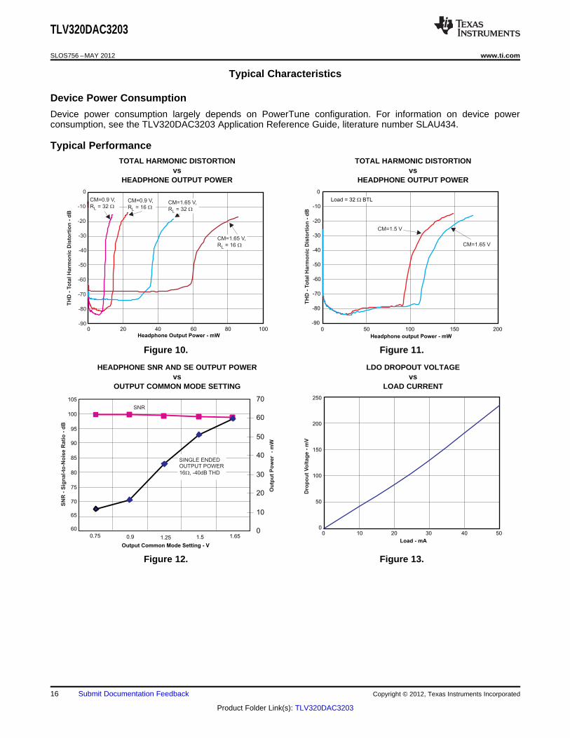
Typical Characteristics
Device Power Consumption
Device power consumption largely depends on PowerTune configuration. For information on device powerconsumption, see the TLV320DAC3203 Application Reference Guide, literature number SLAU434.
Typical PerformanceTOTAL HARMONIC DISTORTION TOTAL HARMONIC DISTORTION
vs vsHEADPHONE OUTPUT POWER HEADPHONE OUTPUT POWER
Figure 10. Figure 11.
HEADPHONE SNR AND SE OUTPUT POWER LDO DROPOUT VOLTAGEvs vs
OUTPUT COMMON MODE SETTING LOAD CURRENT
Figure 12. Figure 13.
16 Submit Documentation Feedback Copyright © 2012, Texas Instruments Incorporated
Product Folder Link(s): TLV320DAC3203

-140
-100
-80
-60
-40
-20
0
0 5000 10000 15000 20000
f - Frequency - Hz
Po
wer
- d
Br
DAC
-120
-140
-100
-80
-60
-40
-20
0
0 5000 10000 15000 20000
f - Frequency - Hz
Po
wer
- d
Br
-120
20
2.4
0 0.5 1 1.5 2 2.5 3
MicBIAS Load - mA
Mic
BIA
S V
olt
ag
e -
mV
2.42
2.44
2.46
2.48
2.5
-20
-40
-10
-30
0
30
10
40
20
0 10 20 30 40 50
Load - mA
Ch
an
ge In
Ou
tpu
t V
olt
ag
e -
mV
TLV320DAC3203
www.ti.com SLOS756 –MAY 2012
MICBIAS MODE 2, CM = 0.9V, LDOIN OP STAGEvs
LDO LOAD RESPONSE MICBIAS LOAD CURRENT
Figure 14. Figure 15.
FFTANALOG BYPASS TO HEADPHONE FFT @ -3dB BELOW
DAC TO HEADPHONE FFT @ -3dBFS 0.5Vrms
Figure 16. Figure 17.
Copyright © 2012, Texas Instruments Incorporated Submit Documentation Feedback 17
Product Folder Link(s): TLV320DAC3203

TLV320DAC3203
SLOS756 –MAY 2012 www.ti.com
Typical Circuit Configuration
Figure 18. Typical Circuit Configuration
Application Overview
The TLV320DAC3203 offers a wide range of configuration options. Figure 1 shows the basic functional blocks ofthe device.
Device Connections
Digital Pins
Only a small number of digital pins are dedicated to a single function; whenever possible, the digital pins have adefault function, and also can be reprogrammed to cover alternative functions for various applications.
The fixed-function pins are Reset and the SPI_Select pin, which are HW control pins. Depending on the state ofSPI_Select, the two control-bus pins SCL/SS and SDA/MOSI are configured for either I2C or SPI protocol.
Other digital IO pins can be configured for various functions via register control. An overview of availablefunctionality is given in Multifunction Pins.
Analog Pins
Analog functions can also be configured to a large degree. For minimum power consumption, analog blocks arepowered down by default. The blocks can be powered up with fine granularity according to the application needs.
Multifunction Pins
Table 7 shows the possible allocation of pins for specific functions. The PLL input, for example, can beprogrammed to be any of 4 pins (MCLK, BCLK, DIN, GPIO).
18 Submit Documentation Feedback Copyright © 2012, Texas Instruments Incorporated
Product Folder Link(s): TLV320DAC3203

TLV320DAC3203
www.ti.com SLOS756 –MAY 2012
Table 7. Multifunction Pin Assignments
1 2 3 4 5 6 7 8
Pin Function MCLK BCLK WCLK DIN DOUT GPIOMFP3/ MFP4/MFP1 MFP2 MFP5SCLK MISO
A PLL Input S (1) S (2) E S (3)
B Codec Clock Input S (1) ,D (4) S (2) S (3)
C I2S BCLK input S (2),D
D I2S BCLK output E (5)
E I2S WCLK input E, D
F I2S WCLK output E
G I2S ADC word clock input E E
H I2S ADC WCLK out E E
I I2S DIN E, D
J I2S DOUT E, D
K General Purpose Output I E
K General Purpose Output II E
K General Purpose Output III E
L General Purpose Input I E
L General Purpose Input II E
L General Purpose Input III E
M INT1 output E E E
N INT2 output E E E
Q Secondary I2S BCLK input E E
R Secondary I2S WCLK in E E
S Secondary I2S DIN E E
T Secondary I2S DOUT E
U Secondary I2S BCLK OUT E E E
V Secondary I2S WCLK OUT E E E
X Aux Clock Output E E E
(1) S(1): The MCLK pin can be used to drive the PLL and Codec Clock inputs simultaneously(2) S(2): The BCLK pin can be used to drive the PLL and Codec Clock and audio interface bit clock inputs simultaneously(3) S(3): The GPIO/MFP5 pin can be used to drive the PLL and Codec Clock inputs simultaneously(4) D: Default Function(5) E: The pin is exclusively used for this function, no other function can be implemented with the same pin (e.g. if GPIO/MFP5 has been
allocated for General Purpose Output, it cannot be used as the INT1 output at the same time)
Analog Audio I/O
The analog I/O path of the TLV320DAC3203 offers a variety of options for signal conditioning and routing:• 2 headphone amplifier outputs• Analog gain setting• Single ended and differential modes
Analog Low Power Bypass
The TLV320DAC3203 offers an analog-bypass mode. An analog signal can be routed from the analog input pinto the output amplifier. Neither the digital-input processing blocks nor the DAC resources are required for suchoperation; this supports low-power operation during analog-bypass mode.
In analog low-power bypass mode, line-level signals can be routed directly from the analog inputs INL to the leftheadphone amplifier (HPL) and INR to HPR.
Copyright © 2012, Texas Instruments Incorporated Submit Documentation Feedback 19
Product Folder Link(s): TLV320DAC3203
TLV320DAC3203
SLOS756 –MAY 2012 www.ti.com
Headphone Outputs
The stereo headphone drivers on pins HPL and HPR can drive loads with impedances down to 16Ω in single-ended AC-coupled headphone configurations, or loads down to 32Ω in differential mode, where a speaker isconnected between HPL and HPR. In single-ended drive configuration these drivers can drive up to 15mWpower into each headphone channel while operating from 1.8V analog supplies. While running from the AVddsupply, the output common-mode of the headphone driver is set by the common-mode setting of analog inputs toallow maximum utilization of the analog supply range while simultaneously providing a higher output-voltageswing. In cases when higher output-voltage swing is required, the headphone amplifiers can run directly from thehigher supply voltage on LDOIN input (up to 3.6V). To use the higher supply voltage for higher output signalswing, the output common-mode can be adjusted to either 1.25V, 1.5V or 1.65V. When the common-modevoltage is configured at 1.65V and LDOIN supply is 3.3V, the headphones can each deliver up to 40mW powerinto a 16Ω load.
The headphone drivers are capable of driving a mixed combination of DAC signal and bypass from analog inputINL and INR. The analog input signals can be attenuated up to 72dB before routing. The level of the DAC signalcan be controlled using the digital volume control of the DAC. To control the output-voltage swing of headphonedrivers, the digital volume control provides a range of –6.0dB to +29.0dB (6) in steps of 1dB. These level controlsare not meant to be used as dynamic volume control, but more to set output levels during initial deviceconfiguration. Refer to for recommendations for using headphone volume control for achieving 0dB gain throughthe DAC channel with various configurations.
Digital Microphone Inteface
The TLV320DAC3203 includes a stereo decimation filter for digital microphone inputs. The stereo recording pathcan be powered up one channel at a time, to support the case where only mono record capability is required.
The digital microphone input path of the TLV320DAC3203 features a large set of options for signal conditioningas well as signal routing:• Stereo decimation filters (PDM input)• Fine gain adjustment of digital channels with 0.1 dB step size• Digital volume control with a range of -12 to +20dB• Mute function
In addition to the standard set of stereo decimation filter features the TLV320DAC3203 also offers the followingspecial functions:• Channel-to-channel phase adjustment• Adaptive filter mode
ADC Processing Blocks — Overview
The TLV320DAC3203 includes a built-in digital decimation filter to process the oversampled data from the PDMinput to generate digital data at Nyquist sampling rate with high dynamic range. The decimation filter can bechosen from three different types, depending on the required frequency response, group delay and samplingrate.
Processing Blocks
The TLV320DAC3203 offers a range of processing blocks which implement various signal processing capabilitiesalong with decimation filtering. These processing blocks give users the choice of how much and what type ofsignal processing they may use and which decimation filter is applied.
Table 8 gives an overview of the available processing blocks and their properties.
The signal processing blocks available are:• First-order IIR• Scalable number of biquad filters• Variable-tap FIR filter
(6) If the device must be placed into 'mute' from the –6.0dB setting, set the device at a gain of –5.0dB first, then place the device into mute.
20 Submit Documentation Feedback Copyright © 2012, Texas Instruments Incorporated
Product Folder Link(s): TLV320DAC3203

TLV320DAC3203
www.ti.com SLOS756 –MAY 2012
The processing blocks are tuned for common cases and can achieve high anti-alias filtering or low-group delay incombination with various signal processing effects such as audio effects and frequency shaping. The availablefirst order IIR, BiQuad and FIR filters have fully user-programmable coefficients. The Resource Class Column(RC) gives an approximate indication of power consumption.
Table 8. Processing Blocks
Processing Channel Decimation 1st Order Number FIR Required ResourceBlocks AOSR ValueFilter IIR Available BiQuads Class
PRB_R1 (1) Stereo A Yes 0 No 128,64 6
PRB_R2 Stereo A Yes 5 No 128,64 8
PRB_R3 Stereo A Yes 0 25-Tap 128,64 8
PRB_R4 Right A Yes 0 No 128,64 3
PRB_R5 Right A Yes 5 No 128,64 4
PRB_R6 Right A Yes 0 25-Tap 128,64 4
PRB_R7 Stereo B Yes 0 No 64 3
PRB_R8 Stereo B Yes 3 No 64 4
PRB_R9 Stereo B Yes 0 20-Tap 64 4
PRB_R10 Right B Yes 0 No 64 2
PRB_R11 Right B Yes 3 No 64 2
PRB_R12 Right B Yes 0 20-Tap 64 2
PRB_R13 Stereo C Yes 0 No 32 3
PRB_R14 Stereo C Yes 5 No 32 4
PRB_R15 Stereo C Yes 0 25-Tap 32 4
PRB_R16 Right C Yes 0 No 32 2
PRB_R17 Right C Yes 5 No 32 2
PRB_R18 Right C Yes 0 25-Tap 32 2
(1) Default
For more detailed information see the TLV320DAC3203 Application Reference Guide
DAC
The TLV320DAC3203 includes a stereo audio DAC supporting data rates from 8kHz to 192kHz. Each channel ofthe stereo audio DAC consists of a signal-processing engine with fixed processing blocks, a digital interpolationfilter, multi-bit digital delta-sigma modulator, and an analog reconstruction filter. The DAC is designed to provideenhanced performance at low sampling rates through increased oversampling and image filtering, therebykeeping quantization noise generated within the delta-sigma modulator and signal images strongly suppressedwithin the audio band to beyond 20kHz. To handle multiple input rates and optimize performance, theTLV320DAC3203 allows the system designer to program the oversampling rates over a wide range from 1 to1024. The system designer can choose higher oversampling ratios for lower input data rates and loweroversampling ratios for higher input data rates.
The TLV320DAC3203 DAC channel includes a built-in digital interpolation filter to generate oversampled data forthe sigma-delta modulator. The interpolation filter can be chosen from three different types depending onrequired frequency response, group delay and sampling rate.
The DAC path of the TLV320DAC3203 features many options for signal conditioning and signal routing:• Digital volume control with a range of -63.5 to +24dB• Mute function• Dynamic range compression (DRC)
In addition to the standard set of DAC features the TLV320DAC3203 also offers the following special features:• Built in sine wave generation (beep generator)• Digital auto mute• Adaptive filter mode
Copyright © 2012, Texas Instruments Incorporated Submit Documentation Feedback 21
Product Folder Link(s): TLV320DAC3203
TLV320DAC3203
SLOS756 –MAY 2012 www.ti.com
DAC Processing Blocks — Overview
The TLV320DAC3203 implements signal processing capabilities and interpolation filtering via processing blocks.These fixed processing blocks give users the choice of how much and what type of signal processing they mayuse and which interpolation filter is applied.
Table 9 gives an overview over all available processing blocks of the DAC channel and their properties.
The signal processing blocks available are:• First-order IIR• Scalable number of biquad filters• 3D – Effect• Beep Generator
The processing blocks are tuned for typical cases and can achieve high image rejection or low group delay incombination with various signal processing effects such as audio effects and frequency shaping. The availablefirst-order IIR and biquad filters have fully user-programmable coefficients. The Resource Class Column (RC)gives an approximate indication of power consumption.
Table 9. Overview – DAC Predefined Processing Blocks
Processing Interpolation Channel 1st Order Num. of DRC 3D Beep ResourceBlock No. Filter IIR Available Biquads Generator Class
PRB_P1 (1) A Stereo No 3 No No No 8
PRB_P2 A Stereo Yes 6 Yes No No 12
PRB_P3 A Stereo Yes 6 No No No 10
PRB_P4 A Left No 3 No No No 4
PRB_P5 A Left Yes 6 Yes No No 6
PRB_P6 A Left Yes 6 No No No 6
PRB_P7 B Stereo Yes 0 No No No 6
PRB_P8 B Stereo No 4 Yes No No 8
PRB_P9 B Stereo No 4 No No No 8
PRB_P10 B Stereo Yes 6 Yes No No 10
PRB_P11 B Stereo Yes 6 No No No 8
PRB_P12 B Left Yes 0 No No No 3
PRB_P13 B Left No 4 Yes No No 4
PRB_P14 B Left No 4 No No No 4
PRB_P15 B Left Yes 6 Yes No No 6
PRB_P16 B Left Yes 6 No No No 4
PRB_P17 C Stereo Yes 0 No No No 3
PRB_P18 C Stereo Yes 4 Yes No No 6
PRB_P19 C Stereo Yes 4 No No No 4
PRB_P20 C Left Yes 0 No No No 2
PRB_P21 C Left Yes 4 Yes No No 3
PRB_P22 C Left Yes 4 No No No 2
PRB_P23 A Stereo No 2 No Yes No 8
PRB_P24 A Stereo Yes 5 Yes Yes No 12
PRB_P25 A Stereo Yes 5 Yes Yes Yes 12
(1) Default
For more detailed information see the TLV320DAC3203 Application Reference Guide.
Powertune
The TLV320DAC3203 features PowerTune, a mechanism to balance power-versus-performance trade-offs at thetime of device configuration. The device can be tuned to minimize power dissipation, to maximize performance,or to an operating point between the two extremes to best fit the application.
22 Submit Documentation Feedback Copyright © 2012, Texas Instruments Incorporated
Product Folder Link(s): TLV320DAC3203

TLV320DAC3203
www.ti.com SLOS756 –MAY 2012
For more detailed information see the TLV320DAC3203 Application Reference Guide.
Digital Audio I/O Interface
Audio data is transferred between the host processor and the TLV320DAC3203 via the digital audio data serialinterface, or audio bus. The audio bus on this device is very flexible, including left or right-justified data options,support for I2S or PCM protocols, programmable data length options, a TDM mode for multichannel operation,very flexible master/slave configurability for each bus clock line, and the ability to communicate with multipledevices within a system directly.
The audio bus of the TLV320DAC3203 can be configured for left or right-justified, I2S, DSP, or TDM modes ofoperation, where communication with standard PCM interfaces is supported within the TDM mode. These modesare all MSB-first, with data width programmable as 16, 20, 24, or 32 bits by configuring Page 0, Register 27,D(5:4). In addition, the word clock and bit clock can be independently configured in either Master or Slave mode,for flexible connectivity to a wide variety of processors. The word clock is used to define the beginning of aframe, and may be programmed as either a pulse or a square-wave signal. The frequency of this clockcorresponds to the DAC sampling frequency.
The bit clock is used to clock in and clock out the digital audio data across the serial bus. When in Master mode,this signal can be programmed to generate variable clock pulses by controlling the bit-clock divider in Page 0,Register 30. The number of bit-clock pulses in a frame may need adjustment to accommodate various word-lengths as well as to support the case when multiple TLV320DAC3203s may share the same audio bus.
The TLV320DAC3203 also includes a feature to offset the position of start of data transfer with respect to theword-clock. This offset can be controlled in terms of number of bit-clocks and can be programmed in Page 0,Register 28.
The TLV320DAC3203 also has the feature of inverting the polarity of the bit-clock used for transferring the audiodata as compared to the default clock polarity used. This feature can be used independently of the mode ofaudio interface chosen. This can be configured via Page 0, Register 29, D(3).
The TLV320DAC3203 includes the programmability to program at what bit clock in a frame does audio databegin. This enables time-division multiplexing (TDM), enabling use of multiple codecs on a single audio bus.When the audio serial data bus is powered down while configured in master mode, the pins associated with theinterface are put into a hi-Z output condition.
By default when the word-clocks and bit-clocks are generated by the TLV320DAC3203, these clocks are activeonly when the DAC is powered up within the device. This is done to save power. However, it also supports afeature when both the word clocks and bit-clocks can be active even when the DAC in the device is powereddown. This is useful when using the TDM mode with multiple codecs on the same bus, or when word-clock or bit-clocks are used in the system as general-purpose clocks.
Clock Generation and PLL
The TLV320DAC3203 supports a wide range of options for generating clocks for the DAC as well as interfaceand other control blocks. The clocks for the DAC require a source reference clock. This clock can be provided ona variety of device pins such as MCLK, BCLK, or GPIO pins. The CODEC_CLKIN can then be routed throughhighly-flexible clock dividers to generate the various clocks required for the DAC sections. In the event that thedesired audio clocks cannot be generated from the reference clocks on MCLK, BCLK, or GPIO, theTLV320DAC3203 also provides the option of using the on-chip PLL, which supports a wide range of fractionalmultiplication values to generate the required clocks. Starting from CODEC_CLKIN the TLV320DAC3203provides several programmable clock dividers to help achieve a variety of sampling rates for the DAC.
For more detailed information see the TLV320DAC3203 Application Reference Guide.
Control Interfaces
The TLV320DAC3203 control interface supports SPI or I2C communication protocols, with the protocol selectableusing the SPI_SELECT pin. For SPI, SPI_SELECT should be tied high; for I2C, SPI_SELECT should be tied low.It is not recommended to change the state of SPI_SELECT during device operation.
Copyright © 2012, Texas Instruments Incorporated Submit Documentation Feedback 23
Product Folder Link(s): TLV320DAC3203

TLV320DAC3203
SLOS756 –MAY 2012 www.ti.com
I2C Control
The TLV320DAC3203 supports the I2C control protocol, and will respond to the I2C address of 0011000. I2C is atwo-wire, open-drain interface supporting multiple devices and masters on a single bus. Devices on the I2C busonly drive the bus lines LOW by connecting them to ground; they never drive the bus lines HIGH. Instead, thebus wires are pulled HIGH by pullup resistors, so the bus wires are HIGH when no device is driving them LOW.This way, two devices cannot conflict; if two devices drive the bus simultaneously, there is no driver contention.
SPI Control
In the SPI control mode, the TLV320DAC3203 uses the pins SCL/SS as SS, SCLK as SCLK, MISO as MISO,SDA/MOSI as MOSI; a standard SPI port with clock polarity setting of 0 (typical microprocessor SPI control bitCPOL = 0). The SPI port allows full-duplex, synchronous, serial communication between a host processor (themaster) and peripheral devices (slaves). The SPI master (in this case, the host processor) generates thesynchronizing clock (driven onto SCLK) and initiates transmissions. The SPI slave devices (such as theTLV320DAC3203) depend on a master to start and synchronize transmissions. A transmission begins wheninitiated by an SPI master. The byte from the SPI master begins shifting in on the slave MOSI pin under thecontrol of the master serial clock (driven onto SCLK). As the byte shifts in on the MOSI pin, a byte shifts out onthe MISO pin to the master shift register.
For more detailed information see the TLV320DAC3203 Application Reference Guide.
Power Supply
For more detailed information see the TLV320DAC3203 Application Reference Guide.
Device Special Functions
The following special functions are available to support advanced system requirements:• Headset detection• Interrupt generation• Flexible pin multiplexing
For more detailed information see the TLV320DAC3203 Application Reference Guide.
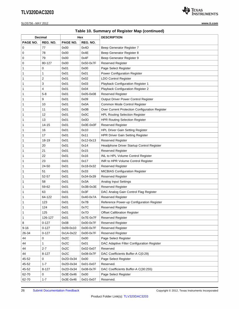
Register Map Summary
Table 10. Summary of Register Map
Decimal Hex DESCRIPTION
PAGE NO. REG. NO. PAGE NO. REG. NO.
0 0 0x00 0x00 Page Select Register
0 1 0x00 0x01 Software Reset Register
0 2 0x00 0x02 Reserved Register
0 3 0x00 0x03 Reserved Register
0 4 0x00 0x04 Clock Setting Register 1, Multiplexers
0 5 0x00 0x05 Clock Setting Register 2, PLL P&R Values
0 6 0x00 0x06 Clock Setting Register 3, PLL J Values
0 7 0x00 0x07 Clock Setting Register 4, PLL D Values (MSB)
0 8 0x00 0x08 Clock Setting Register 5, PLL D Values (LSB)
0 9-10 0x00 0x09-0x0A Reserved Register
0 11 0x00 0x0B Clock Setting Register 6, NDAC Values
0 12 0x00 0x0C Clock Setting Register 7, MDAC Values
0 13 0x00 0x0D DAC OSR Setting Register 1, MSB Value
0 14 0x00 0x0E DAC OSR Setting Register 2, LSB Value
0 15-17 0x00 0x0F-0x11 Reserved Register
0 18 0x00 0x12 Clock Setting Register 8, NADC Values
0 19 0x00 0x13 Clock Setting Register 9, MADC Values
24 Submit Documentation Feedback Copyright © 2012, Texas Instruments Incorporated
Product Folder Link(s): TLV320DAC3203

TLV320DAC3203
www.ti.com SLOS756 –MAY 2012
Table 10. Summary of Register Map (continued)
Decimal Hex DESCRIPTION
PAGE NO. REG. NO. PAGE NO. REG. NO.
0 20-24 0x00 0x14-0x18 Reserved Register
0 25 0x00 0x19 Clock Setting Register 10, Multiplexers
0 26 0x00 0x1A Clock Setting Register 11, CLKOUT M divider value
0 27 0x00 0x1B Audio Interface Setting Register 1
0 28 0x00 0x1C Audio Interface Setting Register 2, Data offset setting
0 29 0x00 0x1D Audio Interface Setting Register 3
0 30 0x00 0x1E Clock Setting Register 12, BCLK N Divider
0 31 0x00 0x1F Audio Interface Setting Register 4, Secondary Audio Interface
0 32 0x00 0x20 Audio Interface Setting Register 5
0 33 0x00 0x21 Audio Interface Setting Register 6
0 34 0x00 0x22 Digital Interface Misc. Setting Register
0 35-36 0x00 0x23-0x24 Reserved Register
0 37 0x00 0x25 DAC Flag Register 1
0 38 0x00 0x26 DAC Flag Register 2
0 39-41 0x00 0x27-0x29 Reserved Register
0 42 0x00 0x2A Sticky Flag Register 1
0 43 0x00 0x2B Interrupt Flag Register 1
0 44 0x00 0x2C Sticky Flag Register 2
0 45 0x00 0x2D Sticky Flag Register 3
0 46 0x00 0x2E Interrupt Flag Register 2
0 47 0x00 0x2F Interrupt Flag Register 3
0 48 0x00 0x30 INT1 Interrupt Control Register
0 49 0x00 0x31 INT2 Interrupt Control Register
0 50-51 0x00 0x32-0x33 Reserved Register
0 52 0x00 0x34 GPIO/MFP5 Control Register (YZK Package only)
0 53 0x00 0x35 MFP2 Function Control Register
0 54 0x00 0x36 DIN/MFP1 Function Control Register
0 55 0x00 0x37 MISO/MFP4 Function Control Register
0 56 0x00 0x38 SCLK/MFP3 Function Control Register
0 57-59 0x00 0x39-0x3B Reserved Registers
0 60 0x00 0x3C DAC Signal Processing Block Control Register
0 61-62 0x00 0x3D-0x3E Reserved Register
0 63 0x00 0x3F DAC Channel Setup Register 1
0 64 0x00 0x40 DAC Channel Setup Register 2
0 65 0x00 0x41 Left DAC Channel Digital Volume Control Register
0 66 0x00 0x42 Right DAC Channel Digital Volume Control Register
0 67 0x00 0x43 Headset Detection Configuration Register
0 68 0x00 0x44 DRC Control Register 1
0 69 0x00 0x45 DRC Control Register 2
0 70 0x00 0x46 DRC Control Register 3
0 71 0x00 0x47 Beep Generator Register 1
0 72 0x00 0x48 Beep Generator Register 2
0 73 0x00 0x49 Beep Generator Register 3
0 74 0x00 0x4A Beep Generator Register 4
0 75 0x00 0x4B Beep Generator Register 5
0 76 0x00 0x4C Beep Generator Register 6
Copyright © 2012, Texas Instruments Incorporated Submit Documentation Feedback 25
Product Folder Link(s): TLV320DAC3203
TLV320DAC3203
SLOS756 –MAY 2012 www.ti.com
Table 10. Summary of Register Map (continued)
Decimal Hex DESCRIPTION
PAGE NO. REG. NO. PAGE NO. REG. NO.
0 77 0x00 0x4D Beep Generator Register 7
0 78 0x00 0x4E Beep Generator Register 8
0 79 0x00 0x4F Beep Generator Register 9
0 80-127 0x00 0x50-0x7F Reserved Register
1 0 0x01 0x00 Page Select Register
1 1 0x01 0x01 Power Configuration Register
1 2 0x01 0x02 LDO Control Register
1 3 0x01 0x03 Playback Configuration Register 1
1 4 0x01 0x04 Playback Configuration Register 2
1 5-8 0x01 0x05-0x08 Reserved Register
1 9 0x01 0x09 Output Driver Power Control Register
1 10 0x01 0x0A Common Mode Control Register
1 11 0x01 0x0B Over Current Protection Configuration Register
1 12 0x01 0x0C HPL Routing Selection Register
1 13 0x01 0x0D HPR Routing Selection Register
1 14-15 0x01 0x0E-0x0F Reserved Register
1 16 0x01 0x10 HPL Driver Gain Setting Register
1 17 0x01 0x11 HPR Driver Gain Setting Register
1 18-19 0x01 0x12-0x13 Reserved Register
1 20 0x01 0x14 Headphone Driver Startup Control Register
1 21 0x01 0x15 Reserved Register
1 22 0x01 0x16 INL to HPL Volume Control Register
1 23 0x01 0x17 INR to HPR Volume Control Register
1 24-50 0x01 0x18-0x32 Reserved Register
1 51 0x01 0x33 MICBIAS Configuration Register
1 52-57 0x01 0x34-0x39 Reserved Register
1 58 0x01 0x3A Analog Input Settings
1 59-62 0x01 0x3B-0x3E Reserved Register
1 63 0x01 0x3F DAC Analog Gain Control Flag Register
1 64-122 0x01 0x40-0x7A Reserved Register
1 123 0x01 0x7B Reference Power-up Configuration Register
1 124 0x01 0x7C Reserved Register
1 125 0x01 0x7D Offset Callibration Register
1 126-127 0x01 0x7E-0x7F Reserved Register
8 0-127 0x08 0x00-0x7F Reserved Register
9-16 0-127 0x09-0x10 0x00-0x7F Reserved Register
26-34 0-127 0x1A-0x22 0x00-0x7F Reserved Register
44 0 0x2C 0x00 Page Select Register
44 1 0x2C 0x01 DAC Adaptive Filter Configuration Register
44 2-7 0x2C 0x02-0x07 Reserved
44 8-127 0x2C 0x08-0x7F DAC Coefficients Buffer-A C(0:29)
45-52 0 0x2D-0x34 0x00 Page Select Register
45-52 1-7 0x2D-0x34 0x01-0x07 Reserved.
45-52 8-127 0x2D-0x34 0x08-0x7F DAC Coefficients Buffer-A C(30:255)
62-70 0 0x3E-0x46 0x00 Page Select Register
62-70 1-7 0x3E-0x46 0x01-0x07 Reserved.
26 Submit Documentation Feedback Copyright © 2012, Texas Instruments Incorporated
Product Folder Link(s): TLV320DAC3203

TLV320DAC3203
www.ti.com SLOS756 –MAY 2012
Table 10. Summary of Register Map (continued)
Decimal Hex DESCRIPTION
PAGE NO. REG. NO. PAGE NO. REG. NO.
62-70 8-127 0x3E-0x46 0x08-0x7F DAC Coefficients Buffer-B C(0:255)
80-114 0-127 0x50-0x72 0x00-0x7F Reserved Register
152-186 0-127 0x98-0xBA 0x00-0x7F Reserved Register
Copyright © 2012, Texas Instruments Incorporated Submit Documentation Feedback 27
Product Folder Link(s): TLV320DAC3203

PACKAGE OPTION ADDENDUM
www.ti.com 16-Dec-2016
Addendum-Page 1
PACKAGING INFORMATION
Orderable Device Status(1)
Package Type PackageDrawing
Pins PackageQty
Eco Plan(2)
Lead/Ball Finish(6)
MSL Peak Temp(3)
Op Temp (°C) Device Marking(4/5)
Samples
TLV320DAC3203IRGER ACTIVE VQFN RGE 24 3000 Green (RoHS& no Sb/Br)
CU NIPDAU |CU NIPDAUAG
Level-2-260C-1 YEAR -40 to 85 DAC3203I
TLV320DAC3203IRGET ACTIVE VQFN RGE 24 250 Green (RoHS& no Sb/Br)
CU NIPDAU |CU NIPDAUAG
Level-2-260C-1 YEAR -40 to 85 DAC3203I
TLV320DAC3203IYZKR ACTIVE DSBGA YZK 25 3000 Green (RoHS& no Sb/Br)
SNAGCU Level-1-260C-UNLIM -40 to 85 DAC3203I
TLV320DAC3203IYZKT ACTIVE DSBGA YZK 25 250 Green (RoHS& no Sb/Br)
SNAGCU Level-1-260C-UNLIM -40 to 85 DAC3203I
(1) The marketing status values are defined as follows:ACTIVE: Product device recommended for new designs.LIFEBUY: TI has announced that the device will be discontinued, and a lifetime-buy period is in effect.NRND: Not recommended for new designs. Device is in production to support existing customers, but TI does not recommend using this part in a new design.PREVIEW: Device has been announced but is not in production. Samples may or may not be available.OBSOLETE: TI has discontinued the production of the device.
(2) Eco Plan - The planned eco-friendly classification: Pb-Free (RoHS), Pb-Free (RoHS Exempt), or Green (RoHS & no Sb/Br) - please check http://www.ti.com/productcontent for the latest availabilityinformation and additional product content details.TBD: The Pb-Free/Green conversion plan has not been defined.Pb-Free (RoHS): TI's terms "Lead-Free" or "Pb-Free" mean semiconductor products that are compatible with the current RoHS requirements for all 6 substances, including the requirement thatlead not exceed 0.1% by weight in homogeneous materials. Where designed to be soldered at high temperatures, TI Pb-Free products are suitable for use in specified lead-free processes.Pb-Free (RoHS Exempt): This component has a RoHS exemption for either 1) lead-based flip-chip solder bumps used between the die and package, or 2) lead-based die adhesive used betweenthe die and leadframe. The component is otherwise considered Pb-Free (RoHS compatible) as defined above.Green (RoHS & no Sb/Br): TI defines "Green" to mean Pb-Free (RoHS compatible), and free of Bromine (Br) and Antimony (Sb) based flame retardants (Br or Sb do not exceed 0.1% by weightin homogeneous material)
(3) MSL, Peak Temp. - The Moisture Sensitivity Level rating according to the JEDEC industry standard classifications, and peak solder temperature.
(4) There may be additional marking, which relates to the logo, the lot trace code information, or the environmental category on the device.
(5) Multiple Device Markings will be inside parentheses. Only one Device Marking contained in parentheses and separated by a "~" will appear on a device. If a line is indented then it is a continuationof the previous line and the two combined represent the entire Device Marking for that device.
(6) Lead/Ball Finish - Orderable Devices may have multiple material finish options. Finish options are separated by a vertical ruled line. Lead/Ball Finish values may wrap to two lines if the finishvalue exceeds the maximum column width.

PACKAGE OPTION ADDENDUM
www.ti.com 16-Dec-2016
Addendum-Page 2
Important Information and Disclaimer:The information provided on this page represents TI's knowledge and belief as of the date that it is provided. TI bases its knowledge and belief on informationprovided by third parties, and makes no representation or warranty as to the accuracy of such information. Efforts are underway to better integrate information from third parties. TI has taken andcontinues to take reasonable steps to provide representative and accurate information but may not have conducted destructive testing or chemical analysis on incoming materials and chemicals.TI and TI suppliers consider certain information to be proprietary, and thus CAS numbers and other limited information may not be available for release.
In no event shall TI's liability arising out of such information exceed the total purchase price of the TI part(s) at issue in this document sold by TI to Customer on an annual basis.

TAPE AND REEL INFORMATION
*All dimensions are nominal
Device PackageType
PackageDrawing
Pins SPQ ReelDiameter
(mm)
ReelWidth
W1 (mm)
A0(mm)
B0(mm)
K0(mm)
P1(mm)
W(mm)
Pin1Quadrant
TLV320DAC3203IRGER VQFN RGE 24 3000 330.0 12.4 4.25 4.25 1.15 8.0 12.0 Q2
TLV320DAC3203IRGET VQFN RGE 24 250 180.0 12.4 4.25 4.25 1.15 8.0 12.0 Q2
TLV320DAC3203IRGET VQFN RGE 24 250 180.0 12.4 4.25 4.25 1.15 8.0 12.0 Q2
TLV320DAC3203IYZKR DSBGA YZK 25 3000 180.0 8.4 2.75 2.75 0.81 4.0 8.0 Q1
TLV320DAC3203IYZKT DSBGA YZK 25 250 180.0 8.4 2.75 2.75 0.81 4.0 8.0 Q1
PACKAGE MATERIALS INFORMATION
www.ti.com 29-Nov-2016
Pack Materials-Page 1

*All dimensions are nominal
Device Package Type Package Drawing Pins SPQ Length (mm) Width (mm) Height (mm)
TLV320DAC3203IRGER VQFN RGE 24 3000 367.0 367.0 35.0
TLV320DAC3203IRGET VQFN RGE 24 250 210.0 185.0 35.0
TLV320DAC3203IRGET VQFN RGE 24 250 210.0 185.0 35.0
TLV320DAC3203IYZKR DSBGA YZK 25 3000 182.0 182.0 20.0
TLV320DAC3203IYZKT DSBGA YZK 25 250 182.0 182.0 20.0
PACKAGE MATERIALS INFORMATION
www.ti.com 29-Nov-2016
Pack Materials-Page 2


D: Max =
E: Max =
2.67 mm, Min =
2.67 mm, Min =
2.61 mm
2.61 mm

IMPORTANT NOTICE
Texas Instruments Incorporated (TI) reserves the right to make corrections, enhancements, improvements and other changes to itssemiconductor products and services per JESD46, latest issue, and to discontinue any product or service per JESD48, latest issue. Buyersshould obtain the latest relevant information before placing orders and should verify that such information is current and complete.TI’s published terms of sale for semiconductor products (http://www.ti.com/sc/docs/stdterms.htm) apply to the sale of packaged integratedcircuit products that TI has qualified and released to market. Additional terms may apply to the use or sale of other types of TI products andservices.Reproduction of significant portions of TI information in TI data sheets is permissible only if reproduction is without alteration and isaccompanied by all associated warranties, conditions, limitations, and notices. TI is not responsible or liable for such reproduceddocumentation. Information of third parties may be subject to additional restrictions. Resale of TI products or services with statementsdifferent from or beyond the parameters stated by TI for that product or service voids all express and any implied warranties for theassociated TI product or service and is an unfair and deceptive business practice. TI is not responsible or liable for any such statements.Buyers and others who are developing systems that incorporate TI products (collectively, “Designers”) understand and agree that Designersremain responsible for using their independent analysis, evaluation and judgment in designing their applications and that Designers havefull and exclusive responsibility to assure the safety of Designers' applications and compliance of their applications (and of all TI productsused in or for Designers’ applications) with all applicable regulations, laws and other applicable requirements. Designer represents that, withrespect to their applications, Designer has all the necessary expertise to create and implement safeguards that (1) anticipate dangerousconsequences of failures, (2) monitor failures and their consequences, and (3) lessen the likelihood of failures that might cause harm andtake appropriate actions. Designer agrees that prior to using or distributing any applications that include TI products, Designer willthoroughly test such applications and the functionality of such TI products as used in such applications.TI’s provision of technical, application or other design advice, quality characterization, reliability data or other services or information,including, but not limited to, reference designs and materials relating to evaluation modules, (collectively, “TI Resources”) are intended toassist designers who are developing applications that incorporate TI products; by downloading, accessing or using TI Resources in anyway, Designer (individually or, if Designer is acting on behalf of a company, Designer’s company) agrees to use any particular TI Resourcesolely for this purpose and subject to the terms of this Notice.TI’s provision of TI Resources does not expand or otherwise alter TI’s applicable published warranties or warranty disclaimers for TIproducts, and no additional obligations or liabilities arise from TI providing such TI Resources. TI reserves the right to make corrections,enhancements, improvements and other changes to its TI Resources. TI has not conducted any testing other than that specificallydescribed in the published documentation for a particular TI Resource.Designer is authorized to use, copy and modify any individual TI Resource only in connection with the development of applications thatinclude the TI product(s) identified in such TI Resource. NO OTHER LICENSE, EXPRESS OR IMPLIED, BY ESTOPPEL OR OTHERWISETO ANY OTHER TI INTELLECTUAL PROPERTY RIGHT, AND NO LICENSE TO ANY TECHNOLOGY OR INTELLECTUAL PROPERTYRIGHT OF TI OR ANY THIRD PARTY IS GRANTED HEREIN, including but not limited to any patent right, copyright, mask work right, orother intellectual property right relating to any combination, machine, or process in which TI products or services are used. Informationregarding or referencing third-party products or services does not constitute a license to use such products or services, or a warranty orendorsement thereof. Use of TI Resources may require a license from a third party under the patents or other intellectual property of thethird party, or a license from TI under the patents or other intellectual property of TI.TI RESOURCES ARE PROVIDED “AS IS” AND WITH ALL FAULTS. TI DISCLAIMS ALL OTHER WARRANTIES ORREPRESENTATIONS, EXPRESS OR IMPLIED, REGARDING RESOURCES OR USE THEREOF, INCLUDING BUT NOT LIMITED TOACCURACY OR COMPLETENESS, TITLE, ANY EPIDEMIC FAILURE WARRANTY AND ANY IMPLIED WARRANTIES OFMERCHANTABILITY, FITNESS FOR A PARTICULAR PURPOSE, AND NON-INFRINGEMENT OF ANY THIRD PARTY INTELLECTUALPROPERTY RIGHTS. TI SHALL NOT BE LIABLE FOR AND SHALL NOT DEFEND OR INDEMNIFY DESIGNER AGAINST ANY CLAIM,INCLUDING BUT NOT LIMITED TO ANY INFRINGEMENT CLAIM THAT RELATES TO OR IS BASED ON ANY COMBINATION OFPRODUCTS EVEN IF DESCRIBED IN TI RESOURCES OR OTHERWISE. IN NO EVENT SHALL TI BE LIABLE FOR ANY ACTUAL,DIRECT, SPECIAL, COLLATERAL, INDIRECT, PUNITIVE, INCIDENTAL, CONSEQUENTIAL OR EXEMPLARY DAMAGES INCONNECTION WITH OR ARISING OUT OF TI RESOURCES OR USE THEREOF, AND REGARDLESS OF WHETHER TI HAS BEENADVISED OF THE POSSIBILITY OF SUCH DAMAGES.Unless TI has explicitly designated an individual product as meeting the requirements of a particular industry standard (e.g., ISO/TS 16949and ISO 26262), TI is not responsible for any failure to meet such industry standard requirements.Where TI specifically promotes products as facilitating functional safety or as compliant with industry functional safety standards, suchproducts are intended to help enable customers to design and create their own applications that meet applicable functional safety standardsand requirements. Using products in an application does not by itself establish any safety features in the application. Designers mustensure compliance with safety-related requirements and standards applicable to their applications. Designer may not use any TI products inlife-critical medical equipment unless authorized officers of the parties have executed a special contract specifically governing such use.Life-critical medical equipment is medical equipment where failure of such equipment would cause serious bodily injury or death (e.g., lifesupport, pacemakers, defibrillators, heart pumps, neurostimulators, and implantables). Such equipment includes, without limitation, allmedical devices identified by the U.S. Food and Drug Administration as Class III devices and equivalent classifications outside the U.S.TI may expressly designate certain products as completing a particular qualification (e.g., Q100, Military Grade, or Enhanced Product).Designers agree that it has the necessary expertise to select the product with the appropriate qualification designation for their applicationsand that proper product selection is at Designers’ own risk. Designers are solely responsible for compliance with all legal and regulatoryrequirements in connection with such selection.Designer will fully indemnify TI and its representatives against any damages, costs, losses, and/or liabilities arising out of Designer’s non-compliance with the terms and provisions of this Notice.
Mailing Address: Texas Instruments, Post Office Box 655303, Dallas, Texas 75265Copyright © 2017, Texas Instruments Incorporated