
Ultra-Low Power Stereo Audio Codec - Analog, linear, and mixed
1FEATURES
APPLICATIONS
DESCRIPTION
PCM2900PCM2902
SLES035E–MARCH 2007–REVISED MARCH 2008
STEREO AUDIO CODEC WITH USB INTERFACE,SINGLE-ENDED ANALOG INPUT/OUTPUT AND S/PDIF
– Pass-Band Ripple = ±0.1 dB234• PCM2900: Without S/PDIF – Stop-Band Attenuation = –43 dB• PCM2902: With S/PDIF – Single-Ended Voltage Output• On-Chip USB Interface: – Analog LPF Included
– With Full-Speed Transceivers • Multifunctions:– Fully Compliant With USB 1.1 Specification – Human Interface Device (HID) Volume ±
Control and Mute Control– Certified by USB-IF– Suspend Flag– Partially Programmable Descriptors (1)
• Package: 28-Pin SSOP– USB Adaptive Mode for Playback– USB Asynchronous Mode for Record– Bus Powered • USB Audio Speaker
• 16-Bit Delta-Sigma ADC and DAC • USB Headset• Sampling Rate: • USB Monitor
– DAC: 32, 44.1, 48 kHz • USB Audio Interface Box– ADC: 8, 11.025, 16, 22.05, 32, 44.1, 48 kHz
• On-Chip Clock Generator With Single 12-MHzClock Source The PCM2900/2902 is Texas Instruments' single-chip
• Single Power Supply: 5 V Typical (VBUS) USB stereo audio codec with USB-compliantfull-speed protocol controller and S/PDIF (only• Stereo ADCPCM2902). The USB protocol controller works with– Analog Performance at VBUS = 5 V no software code, but the USB descriptors can be
– THD+N = 0.01% modified in some areas (e.g., vendor ID/product ID).The PCM2900/2902 employs SpAct™ architecture,– SNR = 89 dBTI's unique system that recovers the audio clock from– Dynamic Range = 89 dB USB packet data. On-chip analog PLLs with SpAct
– Decimation Digital Filter architecture enable playback and record with lowclock jitter and with independent playback and record– Pass-Band Ripple = ±0.05 dBsampling rates.– Stop-Band Attenuation = 65 dB
– Single-Ended Voltage Input– Antialiasing Filter Included– Digital LCF Included
• Stereo DAC– Analog Performance at VBUS = 5 V
– THD+N = 0.005%– SNR = 96 dB– Dynamic Range = 93 dB
– Oversampling Digital Filter(1) The descriptor can be modified by changing a mask.
1
Please be aware that an important notice concerning availability, standard warranty, and use in critical applications ofTexas Instruments semiconductor products and disclaimers thereto appears at the end of this data sheet.
2SpAct is a trademark of Texas Instruments.3System Two, Audio Precision are trademarks of Audio Precision, Inc.4All other trademarks are the property of their respective owners.
PRODUCTION DATA information is current as of publication date. Copyright © 2007–2008, Texas Instruments IncorporatedProducts conform to specifications per the terms of the TexasInstruments standard warranty. Production processing does notnecessarily include testing of all parameters.
Not Recommended for New Designs
www.ti.com
ABSOLUTE MAXIMUM RATINGS
PCM2900PCM2902SLES035E–MARCH 2007–REVISED MARCH 2008
This integrated circuit can be damaged by ESD. Texas Instruments recommends that all integrated circuits be handled withappropriate precautions. Failure to observe proper handling and installation procedures can cause damage.
ESD damage can range from subtle performance degradation to complete device failure. Precision integrated circuits may be moresusceptible to damage because very small parametric changes could cause the device not to meet its published specifications.
PACKAGING ORDERING INFORMATIONPCM2900SPECIFIEDPACKAGE PACKAGE ORDERING TRANSPORTPRODUCT PACKAGE-LEAD TEMPERATUREDESIGNATOR MARKING NUMBER (1) MEDIARANGE
PCM2900E RailsPCM2900E SSOP-28 28DB –25°C to 85°C PCM2900E
PCM2900E/2K Tape and reel
(1) Models with a slash (/) are available only in tape and reel in the quantities indicated (e.g., /2K indicates 2000 devices per reel). Ordering2000 pieces of PCM2900E/2K gets a single 2000-piece tape and reel.
PCM2902SPECIFIEDPACKAGE PACKAGE ORDERING TRANSPORTPRODUCT PACKAGE-LEAD TEMPERATUREDESIGNATOR MARKING NUMBER (1) MEDIARANGE
PCM2902E RailsPCM2902E SSOP-28 28DB –25°C to 85°C PCM2902E
PCM2902E/2K Tape and reel
(1) Models with a slash (/) are available only in tape and reel in the quantities indicated (e.g., /2K indicates 2000 devices per reel). Ordering2000 pieces of PCM2902E/2K gets a single 2000-piece tape and reel.
over operating free-air temperature range (unless otherwise noted) (1)
PCM2900/PCM2902 UNITVBUS Supply voltage –0.3 to 6.5 V
Ground voltage differences, AGNDC, AGNDP, AGNDX, DGND, DGNDU ±0.1 VSEL0, SEL1, TEST0 (DIN) (2) –0.3 to 6.5 V
Digital input voltageD+, D–, HID0, HID1, HID2, XTI, XTO, TEST1 (DOUT) (2), SSPND –0.3 to (VDDI + 0.3) < 4 VVINL, VINR, VCOM, VOUTR, VOUTL –0.3 to (VCCCI + 0.3) < 4 VAnalog input
voltage VCCCI, VCCP1I, VCCP2I, VCCXI, VDDI –0.3 to 4 VInput current (any pins except supplies) ±10 mAAmbient temperature under bias –40 to 125 °C
Tstg Storage temperature –55 to 150 °CTJ Junction temperature 150 °C
Lead temperature (soldering) 260 °C, 5 sPackage temperature (IR reflow, peak) 250 °C
(1) Stresses beyond those listed under absolute maximum ratings may cause permanent damage to the device. These are stress ratingsonly, and functional operation of the device at these or any other conditions beyond those indicated under recommended operatingconditions is not implied. Exposure to absolute-maximum-rated conditions for extended periods may affect device reliability.
(2) ( ): PCM2902
2 Submit Documentation Feedback Copyright © 2007–2008, Texas Instruments Incorporated
Product Folder Link(s): PCM2900 PCM2902
Not Recommended for New Designs
www.ti.com
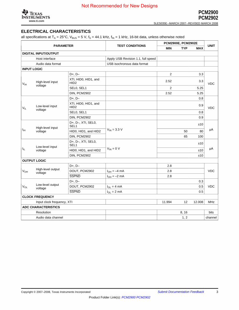
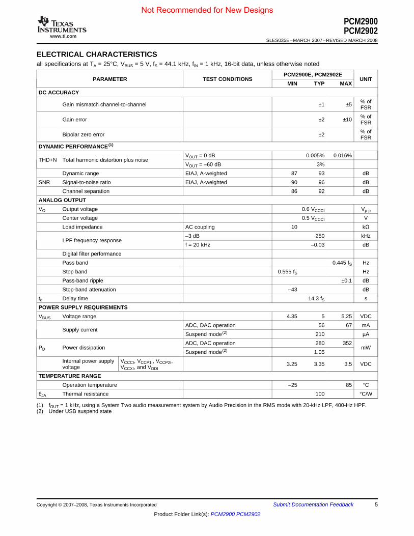
ELECTRICAL CHARACTERISTICS
PCM2900PCM2902
SLES035E–MARCH 2007–REVISED MARCH 2008
all specifications at TA = 25°C, VBUS = 5 V, fS = 44.1 kHz, fIN = 1 kHz, 16-bit data, unless otherwise noted
PCM2900E, PCM2902EPARAMETER TEST CONDITIONS UNIT
MIN TYP MAXDIGITAL INPUT/OUTPUT
Host interface Apply USB Revision 1.1, full speedAudio data format USB isochronous data format
INPUT LOGICD+, D– 2 3.3XTI, HID0, HID1, and 2.52 3.3High-level input HID2VIH VDCvoltageSEL0, SEL1 2 5.25DIN, PCM2902 2.52 5.25D+, D– 0.8XTI, HID0, HID1, and 0.9Low-level input HID2VIL VDCvoltageSEL0, SEL1 0.8DIN, PCM2902 0.9D+, D–, XTI, SEL0, ±10SEL1High-level inputIIH VIN = 3.3 V µAvoltage HID0, HID1, and HID2 50 80DIN, PCM2902 65 100D+, D–, XTI, SEL0, ±10SEL1Low-level inputIIL VIN = 0 V µAvoltage HID0, HID1, and HID2 ±10DIN, PCM2902 ±10
OUTPUT LOGICD+, D– 2.8
High-level outputVOH DOUT, PCM2902 IOH = –4 mA 2.8 VDCvoltageSSPND IOH = –2 mA 2.8D+, D– 0.3
Low-level outputVOL DOUT, PCM2902 IOL = 4 mA 0.5 VDCvoltageSSPND IOL = 2 mA 0.5
CLOCK FREQUENCYInput clock frequency, XTI 11.994 12 12.008 MHz
ADC CHARACTERISTICSResolution 8, 16 bitsAudio data channel 1, 2 channel
Copyright © 2007–2008, Texas Instruments Incorporated Submit Documentation Feedback 3
Product Folder Link(s): PCM2900 PCM2902
Not Recommended for New Designs
www.ti.com
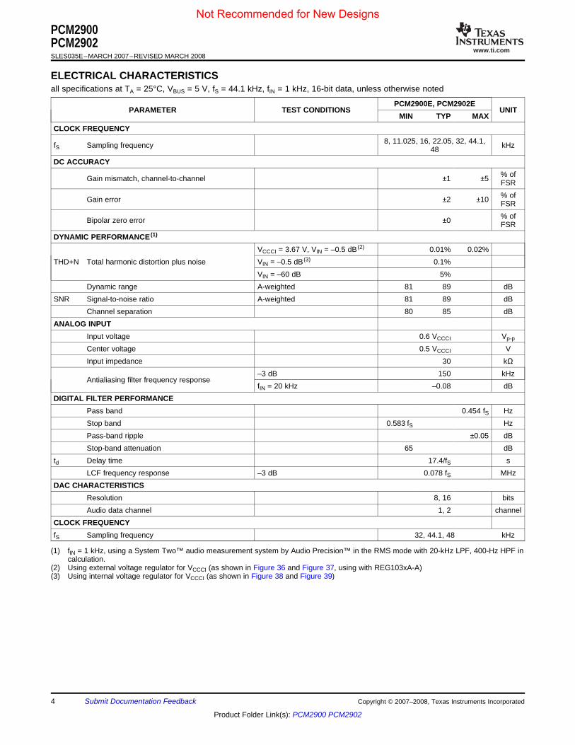
ELECTRICAL CHARACTERISTICS
PCM2900PCM2902SLES035E–MARCH 2007–REVISED MARCH 2008
all specifications at TA = 25°C, VBUS = 5 V, fS = 44.1 kHz, fIN = 1 kHz, 16-bit data, unless otherwise noted
PCM2900E, PCM2902EPARAMETER TEST CONDITIONS UNIT
MIN TYP MAXCLOCK FREQUENCY
8, 11.025, 16, 22.05, 32, 44.1,fS Sampling frequency kHz48DC ACCURACY
% ofGain mismatch, channel-to-channel ±1 ±5 FSR% ofGain error ±2 ±10 FSR% ofBipolar zero error ±0 FSR
DYNAMIC PERFORMANCE (1)
VCCCI = 3.67 V, VIN = –0.5 dB (2) 0.01% 0.02%THD+N Total harmonic distortion plus noise VIN = –0.5 dB (3) 0.1%
VIN = –60 dB 5%Dynamic range A-weighted 81 89 dB
SNR Signal-to-noise ratio A-weighted 81 89 dBChannel separation 80 85 dB
ANALOG INPUTInput voltage 0.6 VCCCI Vp-p
Center voltage 0.5 VCCCI VInput impedance 30 kΩ
–3 dB 150 kHzAntialiasing filter frequency response
fIN = 20 kHz –0.08 dBDIGITAL FILTER PERFORMANCE
Pass band 0.454 fS HzStop band 0.583 fS HzPass-band ripple ±0.05 dBStop-band attenuation 65 dB
td Delay time 17.4/fS sLCF frequency response –3 dB 0.078 fS MHz
DAC CHARACTERISTICSResolution 8, 16 bitsAudio data channel 1, 2 channel
CLOCK FREQUENCYfS Sampling frequency 32, 44.1, 48 kHz
(1) fIN = 1 kHz, using a System Two™ audio measurement system by Audio Precision™ in the RMS mode with 20-kHz LPF, 400-Hz HPF incalculation.
(2) Using external voltage regulator for VCCCI (as shown in Figure 36 and Figure 37, using with REG103xA-A)(3) Using internal voltage regulator for VCCCI (as shown in Figure 38 and Figure 39)
4 Submit Documentation Feedback Copyright © 2007–2008, Texas Instruments Incorporated
Product Folder Link(s): PCM2900 PCM2902
Not Recommended for New Designs
www.ti.com
ELECTRICAL CHARACTERISTICS
PCM2900PCM2902
SLES035E–MARCH 2007–REVISED MARCH 2008
all specifications at TA = 25°C, VBUS = 5 V, fS = 44.1 kHz, fIN = 1 kHz, 16-bit data, unless otherwise noted
PCM2900E, PCM2902EPARAMETER TEST CONDITIONS UNIT
MIN TYP MAXDC ACCURACY
% ofGain mismatch channel-to-channel ±1 ±5 FSR% ofGain error ±2 ±10 FSR% ofBipolar zero error ±2 FSR
DYNAMIC PERFORMANCE (1)
VOUT = 0 dB 0.005% 0.016%THD+N Total harmonic distortion plus noise
VOUT = –60 dB 3%Dynamic range EIAJ, A-weighted 87 93 dB
SNR Signal-to-noise ratio EIAJ, A-weighted 90 96 dBChannel separation 86 92 dB
ANALOG OUTPUTVO Output voltage 0.6 VCCCI Vp-p
Center voltage 0.5 VCCCI VLoad impedance AC coupling 10 kΩ
–3 dB 250 kHzLPF frequency response
f = 20 kHz –0.03 dBDigital filter performancePass band 0.445 fS HzStop band 0.555 fS HzPass-band ripple ±0.1 dBStop-band attenuation –43 dB
td Delay time 14.3 fS sPOWER SUPPLY REQUIREMENTSVBUS Voltage range 4.35 5 5.25 VDC
ADC, DAC operation 56 67 mASupply current
Suspend mode (2) 210 µAADC, DAC operation 280 352
PD Power dissipation mWSuspend mode (2) 1.05
Internal power supply VCCCI, VCCP1I, VCCP2I, 3.25 3.35 3.5 VDCvoltage VCCXI, and VDDI
TEMPERATURE RANGEOperation temperature –25 85 °C
θJA Thermal resistance 100 °C/W
(1) fOUT = 1 kHz, using a System Two audio measurement system by Audio Precision in the RMS mode with 20-kHz LPF, 400-Hz HPF.(2) Under USB suspend state
Copyright © 2007–2008, Texas Instruments Incorporated Submit Documentation Feedback 5
Product Folder Link(s): PCM2900 PCM2902
Not Recommended for New Designs
www.ti.com
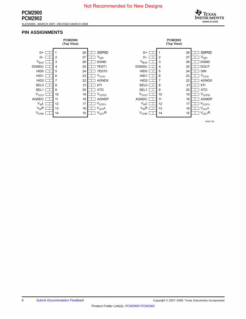
PIN ASSIGNMENTS
1
2
3
4
5
6
7
8
9
10
11
12
13
14
28
27
26
25
24
23
22
21
20
19
18
17
16
15
D+
D–
VBUS
DGNDU
HID0
HID1
HID2
SEL0
SEL1
VCCCI
AGNDC
V LIN
V RIN
VCOM
SSPND
TEST0
VCCXI
AGNDX
XTO
VCCP2I
DGND
VCCP1I
V LOUT
XTI
TEST1
VDDI
AGNDP
V ROUT
PCM2900(Top View)
1
2
3
4
5
6
7
8
9
10
11
12
13
14
28
27
26
25
24
23
22
21
20
19
18
17
16
15
D+
D–
VBUS
DGNDU
HID0
HID1
HID2
SEL0
SEL1
VCCCI
AGNDC
V LIN
V RIN
VCOM
SSPND
DIN
VCCXI
AGNDX
XTO
VCCP2I
DGND
VCCP1I
V LOUT
XTI
DOUT
VDDI
AGNDP
V ROUT
P0007-06
PCM2902(Top View)
PCM2900PCM2902SLES035E–MARCH 2007–REVISED MARCH 2008
6 Submit Documentation Feedback Copyright © 2007–2008, Texas Instruments Incorporated
Product Folder Link(s): PCM2900 PCM2902
Not Recommended for New Designs
www.ti.com
PCM2900PCM2902
SLES035E–MARCH 2007–REVISED MARCH 2008
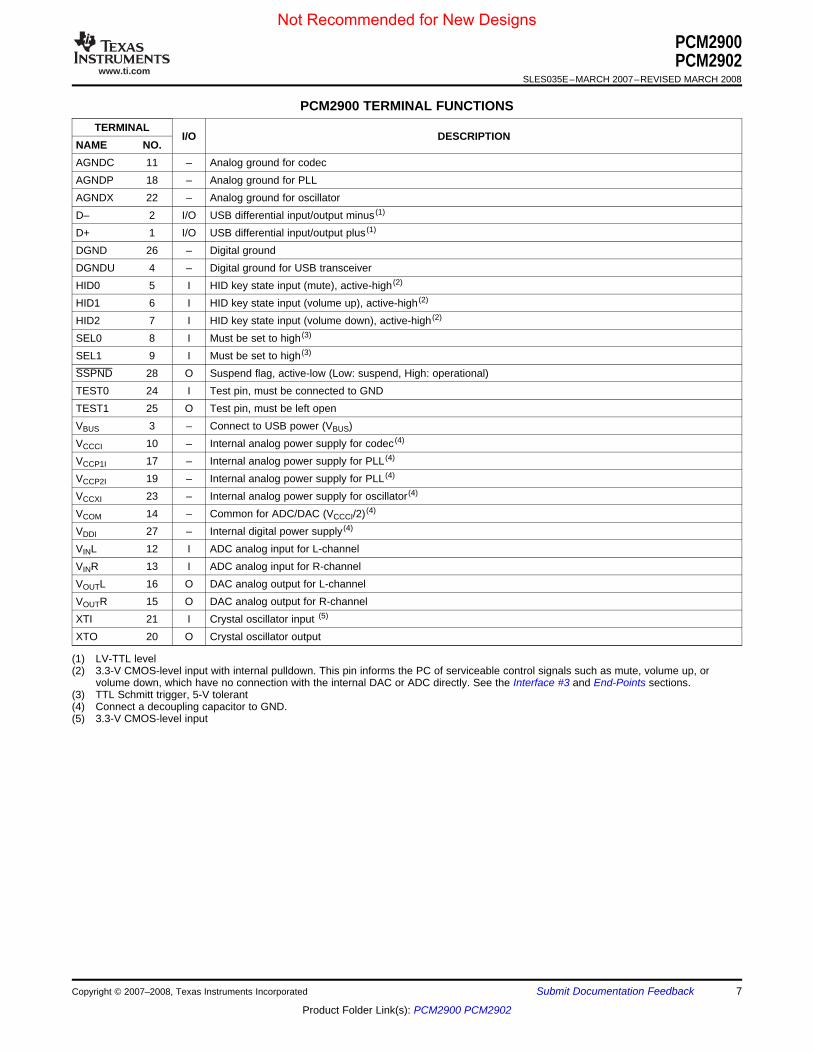
PCM2900 TERMINAL FUNCTIONSTERMINAL
I/O DESCRIPTIONNAME NO.AGNDC 11 – Analog ground for codecAGNDP 18 – Analog ground for PLLAGNDX 22 – Analog ground for oscillatorD– 2 I/O USB differential input/output minus (1)
D+ 1 I/O USB differential input/output plus (1)
DGND 26 – Digital groundDGNDU 4 – Digital ground for USB transceiverHID0 5 I HID key state input (mute), active-high (2)
HID1 6 I HID key state input (volume up), active-high (2)
HID2 7 I HID key state input (volume down), active-high (2)
SEL0 8 I Must be set to high (3)
SEL1 9 I Must be set to high (3)
SSPND 28 O Suspend flag, active-low (Low: suspend, High: operational)TEST0 24 I Test pin, must be connected to GNDTEST1 25 O Test pin, must be left openVBUS 3 – Connect to USB power (VBUS)VCCCI 10 – Internal analog power supply for codec (4)
VCCP1I 17 – Internal analog power supply for PLL (4)
VCCP2I 19 – Internal analog power supply for PLL (4)
VCCXI 23 – Internal analog power supply for oscillator (4)
VCOM 14 – Common for ADC/DAC (VCCCI/2) (4)
VDDI 27 – Internal digital power supply (4)
VINL 12 I ADC analog input for L-channelVINR 13 I ADC analog input for R-channelVOUTL 16 O DAC analog output for L-channelVOUTR 15 O DAC analog output for R-channelXTI 21 I Crystal oscillator input (5)
XTO 20 O Crystal oscillator output
(1) LV-TTL level(2) 3.3-V CMOS-level input with internal pulldown. This pin informs the PC of serviceable control signals such as mute, volume up, or
volume down, which have no connection with the internal DAC or ADC directly. See the Interface #3 and End-Points sections.(3) TTL Schmitt trigger, 5-V tolerant(4) Connect a decoupling capacitor to GND.(5) 3.3-V CMOS-level input
Copyright © 2007–2008, Texas Instruments Incorporated Submit Documentation Feedback 7
Product Folder Link(s): PCM2900 PCM2902
Not Recommended for New Designs
www.ti.com
PCM2900PCM2902SLES035E–MARCH 2007–REVISED MARCH 2008
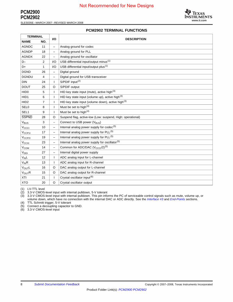
PCM2902 TERMINAL FUNCTIONSTERMINAL
I/O DESCRIPTIONNAME NO.AGNDC 11 – Analog ground for codecAGNDP 18 – Analog ground for PLLAGNDX 22 – Analog ground for oscillatorD– 2 I/O USB differential input/output minus (1)
D+ 1 I/O USB differential input/output plus (1)
DGND 26 – Digital groundDGNDU 4 – Digital ground for USB transceiverDIN 24 I S/PDIF input (2)
DOUT 25 O S/PDIF outputHID0 5 I HID key state input (mute), active high (3)
HID1 6 I HID key state input (volume up), active high (3)
HID2 7 I HID key state input (volume down), active high (3)
SEL0 8 I Must be set to high (4)
SEL1 9 I Must be set to high (4)
SSPND 28 O Suspend flag, active-low (Low: suspend, High: operational)VBUS 3 – Connect to USB power (VBUS)VCCCI 10 – Internal analog power supply for codec (5)
VCCP1I 17 – Internal analog power supply for PLL (5)
VCCP2I 19 – Internal analog power supply for PLL (5)
VCCXI 23 – Internal analog power supply for oscillator (5)
VCOM 14 – Common for ADC/DAC (VCCCI/2) (5)
VDDI 27 – Internal digital power supplyVINL 12 I ADC analog input for L-channelVINR 13 I ADC analog input for R-channelVOUTL 16 O DAC analog output for L-channelVOUTR 15 O DAC analog output for R-channelXTI 21 I Crystal oscillator input (6)
XTO 20 O Crystal oscillator output
(1) LV-TTL level(2) 3.3-V CMOS-level input with internal pulldown, 5-V tolerant(3) 3.3-V CMOS-level input with internal pulldown. This pin informs the PC of serviceable control signals such as mute, volume up, or
volume down, which have no connection with the internal DAC or ADC directly. See the Interface #3 and End-Points sections.(4) TTL Schmitt trigger, 5-V tolerant(5) Connect a decoupling capacitor to GND.(6) 3.3-V CMOS-level input
8 Submit Documentation Feedback Copyright © 2007–2008, Texas Instruments Incorporated
Product Folder Link(s): PCM2900 PCM2902
Not Recommended for New Designs
www.ti.com
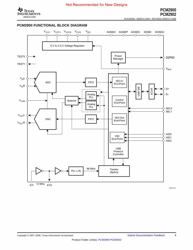
PCM2900 FUNCTIONAL BLOCK DIAGRAM
SSPND
TEST1
ADC
V LIN
V RIN
VCOM
FIFO
Selector
Analog
PLL
Analog
PLL
FIFO
US
B S
IE
XC
VR
DAC
V LOUT
V ROUT
XTI XTO12 MHz
PLL ( 8)´
96 MHz Tracker
(SpAct)
USB
Protocol
Controller
Power
Manager
ISO-In
End-Point
Control
End-Point
ISO-Out
End-Point
HID
End-Point
D+
D–
SEL0
SEL1
HID0
HID1
HID2
VBUS
5-V to 3.3-V Voltage Regulator
VCCCI
VCCP1I
VCCP2I
VCCXI
VDDI DGNDUDGNDAGNDXAGNDPAGNDC
B0238-01
TEST0
PCM2900PCM2902
SLES035E–MARCH 2007–REVISED MARCH 2008
Copyright © 2007–2008, Texas Instruments Incorporated Submit Documentation Feedback 9
Product Folder Link(s): PCM2900 PCM2902
Not Recommended for New Designs
www.ti.com
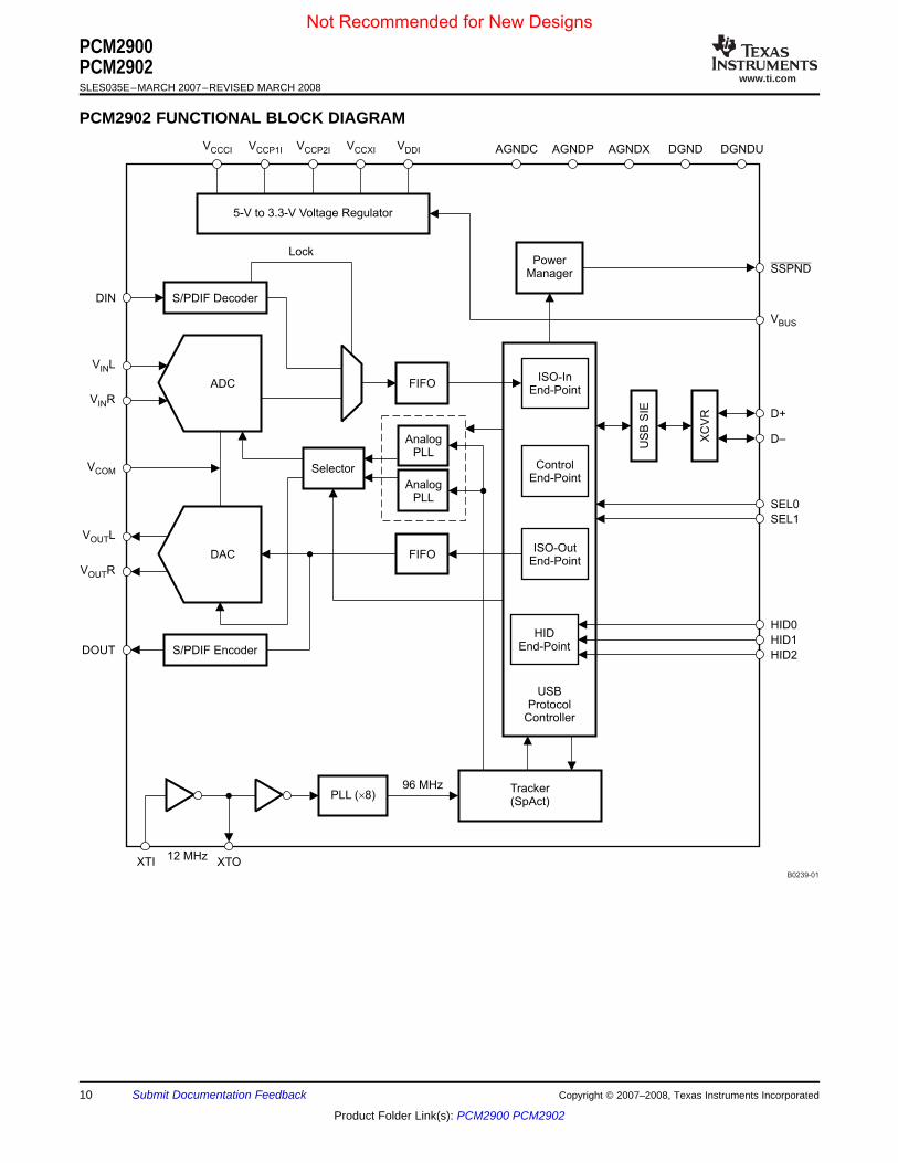
PCM2902 FUNCTIONAL BLOCK DIAGRAM
SSPND
S/PDIF DecoderDIN
Lock
ADC
V LIN
V RIN
VCOM
FIFO
Selector
Analog
PLL
Analog
PLL
FIFO
US
B S
IE
XC
VR
DAC
V LOUT
V ROUT
S/PDIF EncoderDOUT
XTI XTO12 MHz
PLL ( 8)´
96 MHz Tracker
(SpAct)
USB
Protocol
Controller
Power
Manager
ISO-In
End-Point
Control
End-Point
ISO-Out
End-Point
HID
End-Point
D+
D–
SEL0
SEL1
HID0
HID1
HID2
VBUS
5-V to 3.3-V Voltage Regulator
VCCCI
VCCP1I
VCCP2I
VCCXI
VDDI DGNDUDGNDAGNDXAGNDPAGNDC
B0239-01
PCM2900PCM2902SLES035E–MARCH 2007–REVISED MARCH 2008
10 Submit Documentation Feedback Copyright © 2007–2008, Texas Instruments Incorporated
Product Folder Link(s): PCM2900 PCM2902
Not Recommended for New Designs
www.ti.com
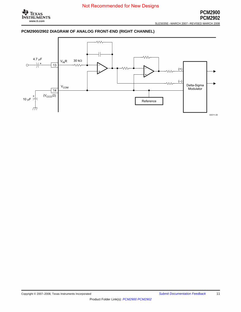
PCM2900/2902 DIAGRAM OF ANALOG FRONT-END (RIGHT CHANNEL)
V RIN
13
14
VCOM
4.7 Fm30 kW
+
+
–
–
Delta-Sigma
Modulator
(+)
(–)
Reference
(V /2)CCCI
10 Fm
+
+
S0011-06
PCM2900PCM2902
SLES035E–MARCH 2007–REVISED MARCH 2008
Copyright © 2007–2008, Texas Instruments Incorporated Submit Documentation Feedback 11
Product Folder Link(s): PCM2900 PCM2902
Not Recommended for New Designs
www.ti.com
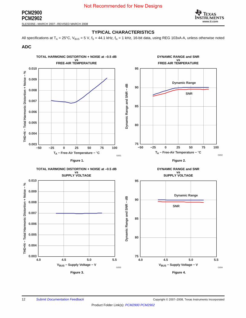
TYPICAL CHARACTERISTICS
ADC
75
80
85
90
95
−50 −25 0 25 50 75 100
TA − Free-Air T emperature − °C
Dyn
amic
Ran
ge a
nd S
NR
− d
B
SNR
Dynamic Range
G002
0.003
0.004
0.005
0.006
0.007
0.008
0.009
0.010
−50 −25 0 25 50 75 100
TA − Free-Air T emperature − °C
TH
D+N
− T
otal
Har
mon
ic D
isto
rtion
+ N
oise
− %
G001
0.003
0.004
0.005
0.006
0.007
0.008
0.009
0.010
4.0 4.5 5.0 5.5
VBUS − Supply V oltage − V
TH
D+N
− T
otal
Har
mon
ic D
isto
rtion
+ N
oise
− %
G003
75
80
85
90
95
4.0 4.5 5.0 5.5
VBUS − Supply V oltage − V
Dyn
amic
Ran
ge a
nd S
NR
− d
B
SNR
Dynamic Range
G004
PCM2900PCM2902SLES035E–MARCH 2007–REVISED MARCH 2008
All specifications at TA = 25°C, VBUS = 5 V, fS = 44.1 kHz, fin = 1 kHz, 16-bit data, using REG 103xA-A, unless otherwise noted
TOTAL HARMONIC DISTORTION + NOISE at –0.5 dB DYNAMIC RANGE and SNRvs vs
FREE-AIR TEMPERATURE FREE-AIR TEMPERATURE
Figure 1. Figure 2.
TOTAL HARMONIC DISTORTION + NOISE at –0.5 dB DYNAMIC RANGE and SNRvs vs
SUPPLY VOLTAGE SUPPLY VOLTAGE
Figure 3. Figure 4.
12 Submit Documentation Feedback Copyright © 2007–2008, Texas Instruments Incorporated
Product Folder Link(s): PCM2900 PCM2902
Not Recommended for New Designs
www.ti.com
75
80
85
90
95
30 35 40 45 50
fS − Sampling Frequency − kHz
Dyn
amic
Ran
ge a
nd S
NR
− d
B
SNR
Dynamic Range
G006
0.03
0.04
0.05
0.06
0.07
0.08
0.09
0.10
30 35 40 45 50
fS − Sampling Frequency − kHz
TH
D+N
− T
otal
Har
mon
ic D
isto
rtion
+ N
oise
− %
0.010
0.009
0.004
0.003
0.005
0.008
0.007
0.006
G005
DAC
90
91
92
93
94
95
96
97
98
−50 −25 0 25 50 75 100
TA − Free-Air T emperature − °C
Dyn
amic
Ran
ge a
nd S
NR
− d
B
SNR
Dynamic Range
G008
0.003
0.004
0.005
0.006
0.007
0.008
−50 −25 0 25 50 75 100
TA − Free-Air T emperature − °C
TH
D+N
− T
otal
Har
mon
ic D
isto
rtion
+ N
oise
− %
G007
PCM2900PCM2902
SLES035E–MARCH 2007–REVISED MARCH 2008
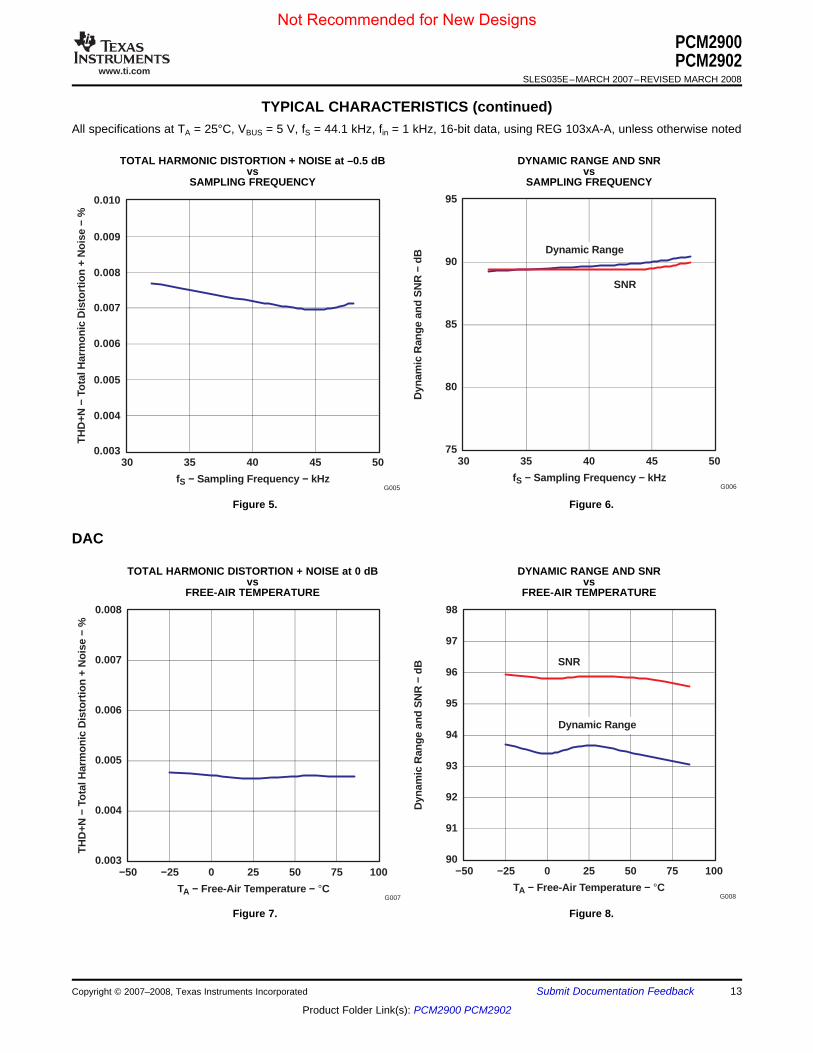
TYPICAL CHARACTERISTICS (continued)All specifications at TA = 25°C, VBUS = 5 V, fS = 44.1 kHz, fin = 1 kHz, 16-bit data, using REG 103xA-A, unless otherwise noted
TOTAL HARMONIC DISTORTION + NOISE at –0.5 dB DYNAMIC RANGE AND SNRvs vs
SAMPLING FREQUENCY SAMPLING FREQUENCY
Figure 5. Figure 6.
TOTAL HARMONIC DISTORTION + NOISE at 0 dB DYNAMIC RANGE AND SNRvs vs
FREE-AIR TEMPERATURE FREE-AIR TEMPERATURE
Figure 7. Figure 8.
Copyright © 2007–2008, Texas Instruments Incorporated Submit Documentation Feedback 13
Product Folder Link(s): PCM2900 PCM2902
Not Recommended for New Designs
www.ti.com
90
91
92
93
94
95
96
97
98
4.0 4.5 5.0 5.5
VBUS − Supply V oltage − V
Dyn
amic
Ran
ge a
nd S
NR
− d
B
SNR
Dynamic Range
G010
0.003
0.004
0.005
0.006
0.007
0.008
4.0 4.5 5.0 5.5
VBUS − Supply V oltage − V
TH
D+N
− T
otal
Har
mon
ic D
isto
rtion
+ N
oise
− %
G009
90
91
92
93
94
95
96
97
98
30 35 40 45 50
fS − Sampling Frequency − kHz
Dyn
amic
Ran
ge a
nd S
NR
− d
B
SNR
Dynamic Range
G012
0.003
0.004
0.005
0.006
0.007
0.008
30 35 40 45 50
fS − Sampling Frequency − kHz
TH
D+N
− T
otal
Har
mon
ic D
isto
rtion
+ N
oise
− %
G011
PCM2900PCM2902SLES035E–MARCH 2007–REVISED MARCH 2008
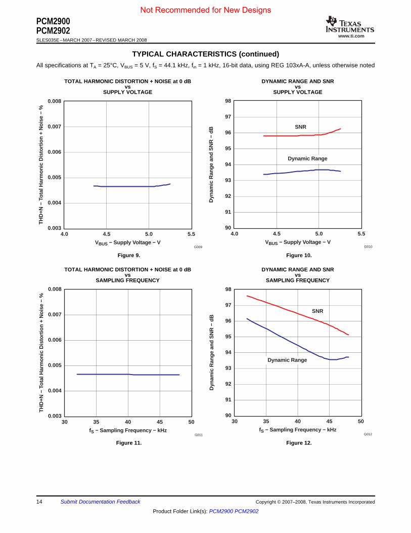
TYPICAL CHARACTERISTICS (continued)All specifications at TA = 25°C, VBUS = 5 V, fS = 44.1 kHz, fin = 1 kHz, 16-bit data, using REG 103xA-A, unless otherwise noted
TOTAL HARMONIC DISTORTION + NOISE at 0 dB DYNAMIC RANGE AND SNRvs vs
SUPPLY VOLTAGE SUPPLY VOLTAGE
Figure 9. Figure 10.
TOTAL HARMONIC DISTORTION + NOISE at 0 dB DYNAMIC RANGE AND SNRvs vs
SAMPLING FREQUENCY SAMPLING FREQUENCY
Figure 11. Figure 12.
14 Submit Documentation Feedback Copyright © 2007–2008, Texas Instruments Incorporated
Product Folder Link(s): PCM2900 PCM2902
Not Recommended for New Designs
www.ti.com
SUPPLY CURRENT
0.20
0.22
0.24
0.26
0.28
0.30
4.00 4.25 4.50 4.75 5.00 5.25 5.50
VBUS − Supply V oltage − V
20
30
40
50
60
70
G013
I CC
− O
pera
tiona
l Sup
ply
Cur
rent
− m
A
I CC
− S
uspe
nd S
uppl
y C
urre
nt −
mAOperational
Suspend
20
30
40
50
60
70
30 35 40 45 50
fS − Sampling Frequency − kHz
I CC
− O
pera
tiona
l Sup
ply
Cur
rent
− m
A
ADC and DAC
G014
0.10
0.15
0.20
0.25
0.30
0.35
0.40
−40 −20 0 20 40 60 80 100
TA − Free-Air T emperature − °C
I CC
− S
uspe
nd S
uppl
y C
urre
nt −
mA
USB Spec Limit for Device (0.3 mA)
G015
PCM2900PCM2902
SLES035E–MARCH 2007–REVISED MARCH 2008
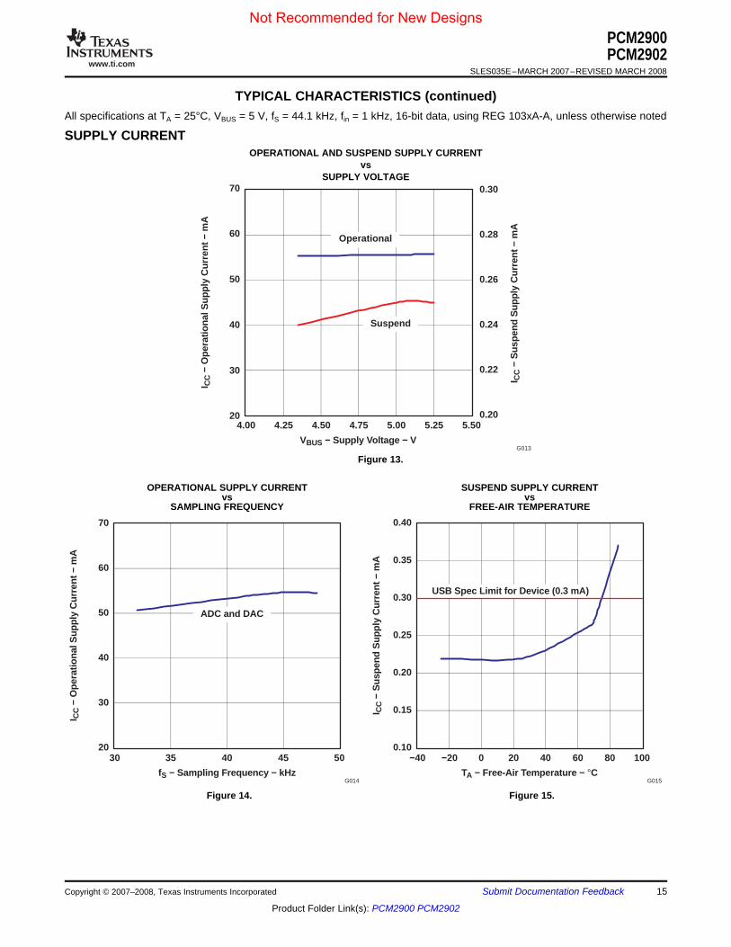
TYPICAL CHARACTERISTICS (continued)All specifications at TA = 25°C, VBUS = 5 V, fS = 44.1 kHz, fin = 1 kHz, 16-bit data, using REG 103xA-A, unless otherwise noted
OPERATIONAL AND SUSPEND SUPPLY CURRENTvs
SUPPLY VOLTAGE
Figure 13.
OPERATIONAL SUPPLY CURRENT SUSPEND SUPPLY CURRENTvs vs
SAMPLING FREQUENCY FREE-AIR TEMPERATURE
Figure 14. Figure 15.
Copyright © 2007–2008, Texas Instruments Incorporated Submit Documentation Feedback 15
Product Folder Link(s): PCM2900 PCM2902
Not Recommended for New Designs
www.ti.com
ADC DIGITAL DECIMATION FILTER FREQUENCY RESPONSE
Frequency [ fS]
−160
−140
−120
−100
−80
−60
−40
−20
0
0 8 16 24 32
Am
plitu
de −
dB
G016Frequency [ fS]
−100
−90
−80
−70
−60
−50
−40
−30
−20
−10
0
0.0 0.2 0.4 0.6 0.8 1.0
Am
plitu
de −
dB
G017
Frequency [ fS]
−20
−16
−12
−8
−4
0
0.46 0.48 0.50 0.52 0.54
Am
plitu
de −
dB
G019Frequency [ fS]
−0.8
−0.6
−0.4
−0.2
0.0
0.2
0.0 0.1 0.2 0.3 0.4 0.5
Am
plitu
de −
dB
0.0
G018
PCM2900PCM2902SLES035E–MARCH 2007–REVISED MARCH 2008
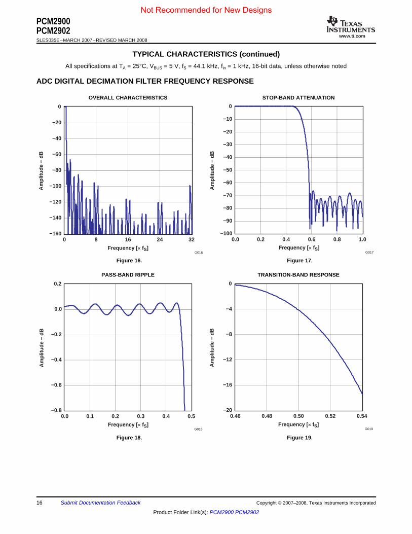
TYPICAL CHARACTERISTICS (continued)All specifications at TA = 25°C, VBUS = 5 V, fS = 44.1 kHz, fin = 1 kHz, 16-bit data, unless otherwise noted
OVERALL CHARACTERISTICS STOP-BAND ATTENUATION
Figure 16. Figure 17.
PASS-BAND RIPPLE TRANSITION-BAND RESPONSE
Figure 18. Figure 19.
16 Submit Documentation Feedback Copyright © 2007–2008, Texas Instruments Incorporated
Product Folder Link(s): PCM2900 PCM2902
Not Recommended for New Designs
www.ti.com
ADC DIGITAL HIGH-PASS FILTER FREQUENCY RESPONSE
Frequency [ fS/1000]
−100
−90
−80
−70
−60
−50
−40
−30
−20
−10
0
0.0 0.1 0.2 0.3 0.4
Am
plitu
de −
dB
G020Frequency [ fS/1000]
−1.0
−0.8
−0.6
−0.4
−0.2
0.0
0 1 2 3 4
Am
plitu
de −
dB
0.0
G021
ADC ANALOG ANTIALIASING FILTER FREQUENCY RESPONSE
−1.0
−0.8
−0.6
−0.4
−0.2
0.0
f − Frequency − kHz
Am
plitu
de −
dB
0.01 1 10 1000.1
0.0
G023
−50
−40
−30
−20
−10
0
f − Frequency − kHz
Am
plitu
de −
dB
1 100 1k 10k10
G022
PCM2900PCM2902
SLES035E–MARCH 2007–REVISED MARCH 2008
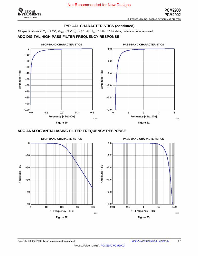
TYPICAL CHARACTERISTICS (continued)All specifications at TA = 25°C, VBUS = 5 V, fS = 44.1 kHz, fin = 1 kHz, 16-bit data, unless otherwise noted
STOP-BAND CHARACTERISTICS PASS-BAND CHARACTERISTICS
Figure 20. Figure 21.
STOP-BAND CHARACTERISTICS PASS-BAND CHARACTERISTICS
Figure 22. Figure 23.
Copyright © 2007–2008, Texas Instruments Incorporated Submit Documentation Feedback 17
Product Folder Link(s): PCM2900 PCM2902
Not Recommended for New Designs
www.ti.com
DAC DIGITAL INTERPOLATION FILTER FREQUENCY RESPONSE
Frequency [ fS]
−100
−90
−80
−70
−60
−50
−40
−30
−20
−10
0
0 1 2 3 4
Am
plitu
de −
dB
G024Frequency [ fS]
−0.8
−0.6
−0.4
−0.2
0.0
0.2
0.0 0.1 0.2 0.3 0.4 0.5
Am
plitu
de −
dB
0.0
G025
Frequency [ fS]
−20
−18
−16
−14
−12
−10
−8
−6
−4
−2
0
0.46 0.47 0.48 0.49 0.50 0.51 0.52 0.53 0.54
Am
plitu
de −
dB
G026
PCM2900PCM2902SLES035E–MARCH 2007–REVISED MARCH 2008
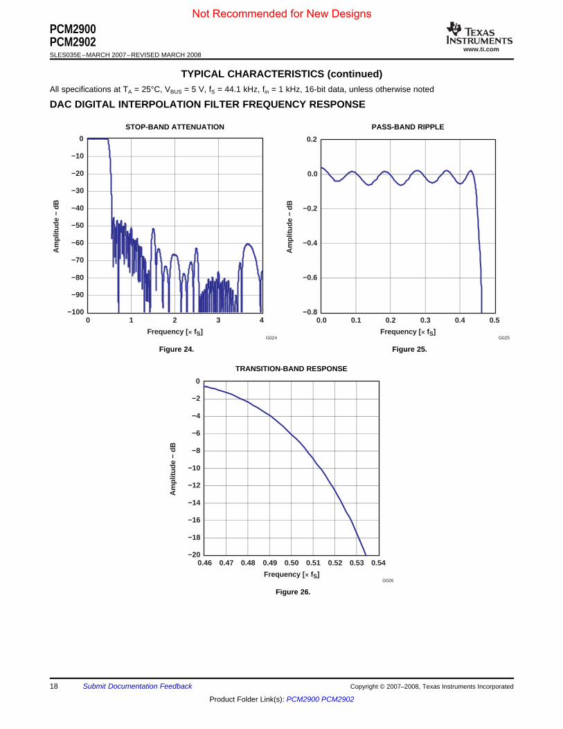
TYPICAL CHARACTERISTICS (continued)All specifications at TA = 25°C, VBUS = 5 V, fS = 44.1 kHz, fin = 1 kHz, 16-bit data, unless otherwise noted
STOP-BAND ATTENUATION PASS-BAND RIPPLE
Figure 24. Figure 25.
TRANSITION-BAND RESPONSE
Figure 26.
18 Submit Documentation Feedback Copyright © 2007–2008, Texas Instruments Incorporated
Product Folder Link(s): PCM2900 PCM2902
Not Recommended for New Designs
www.ti.com
DAC ANALOG FIR FILTER FREQUENCY RESPONSE
−50
−40
−30
−20
−10
0
0 8 16 24 32
Frequency [ fS]
Am
plitu
de −
dB
G027
−0.8
−0.6
−0.4
−0.2
0.0
0.2
0.0 0.1 0.2 0.3 0.4 0.5
Frequency [ fS]
Am
plitu
de −
dB
0.0
G028
DAC ANALOG LOW-PASS FILTER FREQUENCY RESPONSE
−1.0
−0.8
−0.6
−0.4
−0.2
0.0
f − Frequency − kHz
Am
plitu
de −
dB
0.01 1 10 1000.1
0.0
G030
−50
−40
−30
−20
−10
0
f − Frequency − kHz
Am
plitu
de −
dB
1 100 1k 10k10
G029
PCM2900PCM2902
SLES035E–MARCH 2007–REVISED MARCH 2008
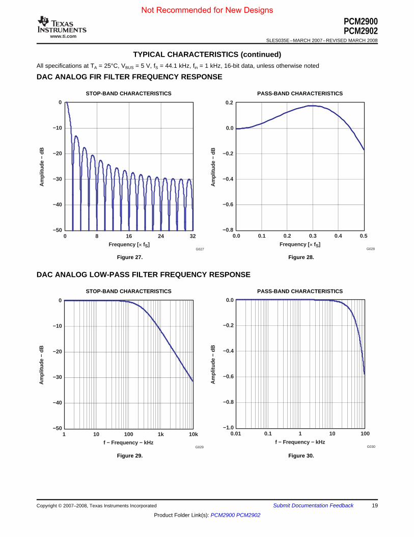
TYPICAL CHARACTERISTICS (continued)All specifications at TA = 25°C, VBUS = 5 V, fS = 44.1 kHz, fin = 1 kHz, 16-bit data, unless otherwise noted
STOP-BAND CHARACTERISTICS PASS-BAND CHARACTERISTICS
Figure 27. Figure 28.
STOP-BAND CHARACTERISTICS PASS-BAND CHARACTERISTICS
Figure 29. Figure 30.
Copyright © 2007–2008, Texas Instruments Incorporated Submit Documentation Feedback 19
Product Folder Link(s): PCM2900 PCM2902
Not Recommended for New Designs
www.ti.com
USB INTERFACE
A
PCM2900PCM2902SLES035E–MARCH 2007–REVISED MARCH 2008
Control data and audio data are transferred to the PCM2900/2902 via D+ (pin 1) and D– (pin 2). All data to/fromthe PCM2900/2902 is transferred at full speed. The device descriptor contains the information described inTable 1. The device descriptor can be modified on request; contact a Texas Instruments representative fordetails.
Table 1. Device DescriptionUSB revision 1.1 compliantDevice class 0x00 (device-defined interface level)Device subclass 0x00 (not specified)Device protocol 0x00 (not specified)Max packet size for end-point 0 8 bytesVendor ID 0x08BB (default value, can be modified)Product ID 0x2900 / 0x2902 (default value, can be modified)Device release number 1.0 (0x0100)Number of configurations 1Vendor strings String #1 (see Table 3)Product strings String #2 (see Table 3)Serial number Not supported
The configuration descriptor contains the information described in Table 2. The configuration descriptor can bemodified on request; contact a Texas Instruments representative for details.
Table 2. Configuration DescriptorInterface Four interfaces
0x80 (Bus powered, no remotePower attribute wakeup)0x32 (100 mA. Default value, can beMax power modified)
The string descriptor contains the information described in Table 3. The string descriptor can be modified onrequest; contact a Texas Instruments representative for details.
Table 3. String Descriptor#0 0x0409#1 Burr-Brown from TI (default value, can be modified)#2 USB audio codec (default value, can be modified)
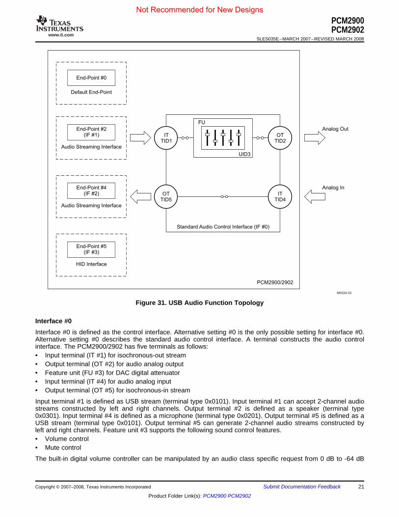
DEVICE CONFIGURATIONFigure 31 illustrates the USB audio function topology. The PCM2900/2902 has four interfaces. Each interface isconstructed by alternative settings.
20 Submit Documentation Feedback Copyright © 2007–2008, Texas Instruments Incorporated
Product Folder Link(s): PCM2900 PCM2902
Not Recommended for New Designs
www.ti.com
Analog Out
Analog In
Default End-Point
End-Point #2
(IF #1)
Audio Streaming Interface
End-Point #0
End-Point #4
(IF #2)
Audio Streaming Interface
End-Point #5
(IF #3)
HID Interface
IT
TID1
FU
UID3
OT
TID5
OT
TID2
IT
TID4
Standard Audio Control Interface (IF #0)
PCM2900/2902
M0024-03
Interface #0
PCM2900PCM2902
SLES035E–MARCH 2007–REVISED MARCH 2008
Figure 31. USB Audio Function Topology
Interface #0 is defined as the control interface. Alternative setting #0 is the only possible setting for interface #0.Alternative setting #0 describes the standard audio control interface. A terminal constructs the audio controlinterface. The PCM2900/2902 has five terminals as follows:• Input terminal (IT #1) for isochronous-out stream• Output terminal (OT #2) for audio analog output• Feature unit (FU #3) for DAC digital attenuator• Input terminal (IT #4) for audio analog input• Output terminal (OT #5) for isochronous-in stream
Input terminal #1 is defined as USB stream (terminal type 0x0101). Input terminal #1 can accept 2-channel audiostreams constructed by left and right channels. Output terminal #2 is defined as a speaker (terminal type0x0301). Input terminal #4 is defined as a microphone (terminal type 0x0201). Output terminal #5 is defined as aUSB stream (terminal type 0x0101). Output terminal #5 can generate 2-channel audio streams constructed byleft and right channels. Feature unit #3 supports the following sound control features.• Volume control• Mute control
The built-in digital volume controller can be manipulated by an audio class specific request from 0 dB to -64 dB
Copyright © 2007–2008, Texas Instruments Incorporated Submit Documentation Feedback 21
Product Folder Link(s): PCM2900 PCM2902
Not Recommended for New Designs
www.ti.com
Interface #1
Interface #2
Interface #3
PCM2900PCM2902SLES035E–MARCH 2007–REVISED MARCH 2008
in 1-dB steps. Changes are made by incrementing or decrementing by one step (1 dB) for every 1/fS time intervaluntil the volume level has reached the requested value. Each channel can be set for different values. The mastervolume control is not supported. A request to the master volume is stalled and ignored. The built-in digital mutecontroller can be manipulated by audio class specific request. A master mute control request is acceptable. Arequest to an individual channel is stalled and ignored.
Interface #1 is the audio streaming data-out interface. Interface #1 has the following seven alternative settings.Alternative setting #0 is the zero bandwidth setting. All other alternative settings are operational settings.
ALTERNATIVE TRANSFER SAMPLING RATEDATA FORMATSETTING MODE (kHz)00 Zero Bandwidth01 16 bit Stereo 2s complement (PCM) Adaptive 32, 44.1, 4802 16 bit Mono 2s complement (PCM) Adaptive 32, 44.1, 4803 8 bit Stereo 2s complement (PCM) Adaptive 32, 44.1, 4804 8 bit Mono 2s complement (PCM) Adaptive 32, 44.1, 4805 8 bit Stereo Offset binary (PCM8) Adaptive 32, 44.1, 4806 8 bit Mono Offset binary (PCM8) Adaptive 32, 44.1, 48
Interface #2 is the audio streaming data-in the interface. Interface #2 has the following 19 alternative settings.Alternative setting #0 is the zero bandwidth setting. All other alternative settings are operational settings.
ALTERNATIVE TRANSFER SAMPLING RATEDATA FORMATSETTING MODE (kHz)00 Zero Bandwidth01 16 bit Stereo 2s complement (PCM) Asynchronous 4802 16 bit Mono 2s complement (PCM) Asynchronous 4803 16 bit Stereo 2s complement (PCM) Asynchronous 44.104 16 bit Mono 2s complement (PCM) Asynchronous 44.105 16 bit Stereo 2s complement (PCM) Asynchronous 3206 16 bit Mono 2s complement (PCM) Asynchronous 3207 16 bit Stereo 2s complement (PCM) Asynchronous 22.0508 16 bit Mono 2s complement (PCM) Asynchronous 22.0509 16 bit Stereo 2s complement (PCM) Asynchronous 160A 16 bit Mono 2s complement (PCM) Asynchronous 160B 8 bit Stereo 2s complement (PCM) Asynchronous 160C 8 bit Mono 2s complement (PCM) Asynchronous 160D 8 bit Stereo 2s complement (PCM) Asynchronous 80E 8 bit Mono 2s complement (PCM) Asynchronous 80F 16 bit Stereo 2s complement (PCM) Synchronous 11.02510 16 bit Mono 2s complement (PCM) Synchronous 11.02511 8 bit Stereo 2s complement (PCM) Synchronous 11.02512 8 bit Mono 2s complement (PCM) Synchronous 11.025
Interface #3 is the interrupt data-in interface. Alternative setting #0 is the only possible setting for interface #3.Interface #3 constructs the HID consumer control device and reports the following three key statuses.• Mute (0xE209)• Volume up (0xE909)• Volume down (0xEA09)
22 Submit Documentation Feedback Copyright © 2007–2008, Texas Instruments Incorporated
Product Folder Link(s): PCM2900 PCM2902
Not Recommended for New Designs
www.ti.com
End-Points
Clock and Reset
Digital Audio Interface (PCM2902)
Supported Input Data (PCM2902)
PCM2900PCM2902
SLES035E–MARCH 2007–REVISED MARCH 2008
The PCM2900/2902 has the following four end-points.• Control end-point (EP #0)• Isochronous-out audio data stream end-point (EP #2)• Isochronous-in audio data stream end-point (EP #4)• HID end-point (EP #5)
The control end-point is a default end-point. The control end-point is used to control all functions of thePCM2900/2902 by the standard USB request and USB audio class specific request from the host. Theisochronous-out audio data stream end-point is an audio sink end-point, which receives the PCM audio data. Theisochronous-out audio data stream end-point accepts the adaptive transfer mode. The isochronous-in audio datastream end-point is an audio source end-point, which transmits the PCM audio data. The isochronous-in audiodata stream end-point uses asynchronous transfer mode. The HID end-point is an interrupt-in end-point. HIDend-point reports HID0, HID1, and HID2 pin status every 32 ms.
The human interface device (HID) pins are defined as consumer control devices. The HID function is designedas an independent end-point from both isochronous-in and -out end-points. This means that the result ofaffection for the HID operation depends on the host software. Typically, the HID function is affected for theprimary audio-out device.
The PCM2900/2902 requires a 12-MHz (±500 ppm) clock for the USB and audio function, which can begenerated by a built-in crystal oscillator with a 12-MHz crystal resonator. The 12-MHz crystal resonator must beconnected to XTI (pin 21) and XTO (pin 20) with one high (1-MΩ) resistor and two small capacitors, thecapacitance of which depends on the load capacitance of the crystal resonator. The external clock can besupplied from XTI (pin 21). If the external clock is supplied, XTO (pin 20) must be left open. Because of noclock-disabling signal, it is not recommended to use the external clock supply. SSPND (pin 28) is unable to useclock disabling.
The PCM2900/2902 has an internal power-on reset circuit, which works automatically when VBUS (pin 3) exceeds2.5 V typical (2.7 V–2.2 V), and about 700 µs is required until internal reset release.
The PCM2902 employs both S/PDIF input and output. Isochronous-out data from the host is encoded to theS/PDIF output and the DAC analog output. Input data is selected as either S/PDIF or ADC analog input. Whenthe device detects an S/PDIF input and successfully locks the received data, the isochronous-in transfer datasource is automatically selected from S/PDIF itself; otherwise, the data source is selected to ADC analog input.
The following data formats are accepted by the S/PDIF input and output. All other data formats are unable to useS/PDIF.• 48-kHz 16-bit stereo• 44.1-kHz 16-bit stereo• 32-kHz 16-bit stereo
Mismatch between input data format and host command may cause unexpected results except in the followingconditions.• Record monaural format from stereo data input at the same data rate• Record 8-bit format from 16-bit data input at the same data rate
A combination between the above conditions is not accepted.
For the playback, all possible data rate source is converted to 16-bit stereo format at the same source data rate.
Copyright © 2007–2008, Texas Instruments Incorporated Submit Documentation Feedback 23
Product Folder Link(s): PCM2900 PCM2902
Not Recommended for New Designs
www.ti.com
Channel Status Information (PCM2902)
Copyright Management (PCM2902)
INTERFACE SEQUENCE
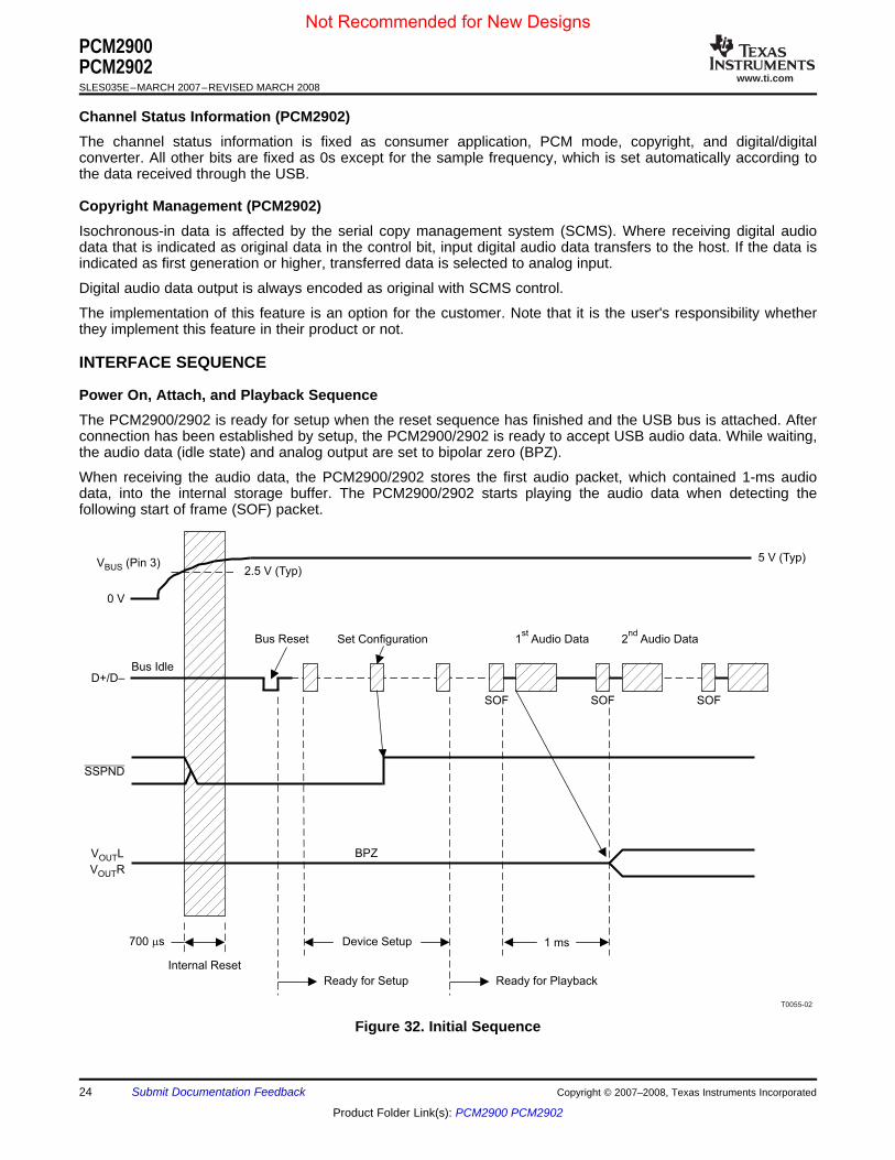
Power On, Attach, and Playback Sequence
D+/D–
2.5 V (Typ)
0 V
Internal Reset
Ready for Setup
SOF
Ready for Playback
Bus Reset Set Configuration
SOF SOF
BPZ
Bus Idle
5 V (Typ)
1 Audio Datast
2 Audio Datand
V (Pin 3)BUS
SSPND
V LOUT
V ROUT
700 sm Device Setup 1 ms
T0055-02
PCM2900PCM2902SLES035E–MARCH 2007–REVISED MARCH 2008
The channel status information is fixed as consumer application, PCM mode, copyright, and digital/digitalconverter. All other bits are fixed as 0s except for the sample frequency, which is set automatically according tothe data received through the USB.
Isochronous-in data is affected by the serial copy management system (SCMS). Where receiving digital audiodata that is indicated as original data in the control bit, input digital audio data transfers to the host. If the data isindicated as first generation or higher, transferred data is selected to analog input.
Digital audio data output is always encoded as original with SCMS control.
The implementation of this feature is an option for the customer. Note that it is the user's responsibility whetherthey implement this feature in their product or not.
The PCM2900/2902 is ready for setup when the reset sequence has finished and the USB bus is attached. Afterconnection has been established by setup, the PCM2900/2902 is ready to accept USB audio data. While waiting,the audio data (idle state) and analog output are set to bipolar zero (BPZ).
When receiving the audio data, the PCM2900/2902 stores the first audio packet, which contained 1-ms audiodata, into the internal storage buffer. The PCM2900/2902 starts playing the audio data when detecting thefollowing start of frame (SOF) packet.
Figure 32. Initial Sequence
24 Submit Documentation Feedback Copyright © 2007–2008, Texas Instruments Incorporated
Product Folder Link(s): PCM2900 PCM2902
Not Recommended for New Designs
www.ti.com
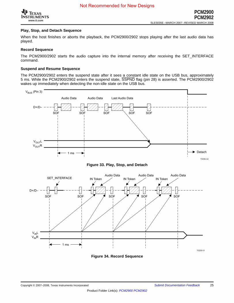
Play, Stop, and Detach Sequence
Record Sequence
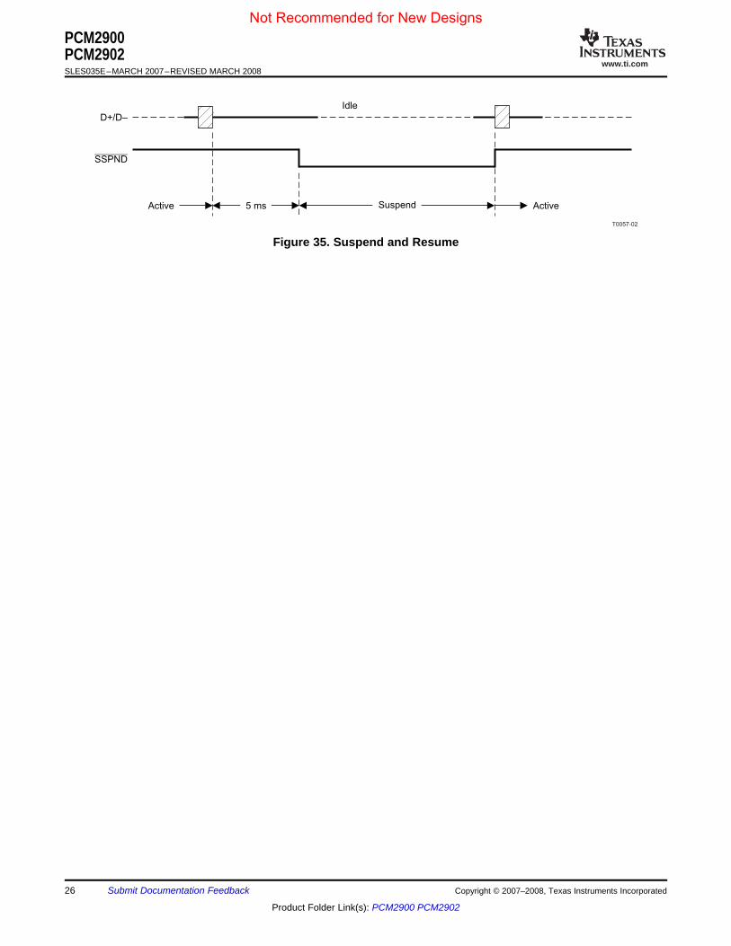
Suspend and Resume Sequence
D+/D–
V LOUT
V ROUT
Audio DataAudio Data Last Audio Data
Detach
SOF SOF SOF SOF SOF
1 ms
V (Pin 3)BUS
T0056-02
D+/D–
V LIN
V RIN
1 ms
SET_INTERFACEAudio Data
IN Token
Audio Data
IN Token
Audio Data
IN Token
SOF SOF SOF SOF SOF
T0259-01
PCM2900PCM2902
SLES035E–MARCH 2007–REVISED MARCH 2008
When the host finishes or aborts the playback, the PCM2900/2902 stops playing after the last audio data hasplayed.
The PCM2900/2902 starts the audio capture into the internal memory after receiving the SET_INTERFACEcommand.
The PCM2900/2902 enters the suspend state after it sees a constant idle state on the USB bus, approximately5 ms. While the PCM2900/2902 enters the suspend state, SSPND flag (pin 28) is asserted. The PCM2900/2902wakes up immediately when detecting the non-idle state on the USB bus.
Figure 33. Play, Stop, and Detach
Figure 34. Record Sequence
Copyright © 2007–2008, Texas Instruments Incorporated Submit Documentation Feedback 25
Product Folder Link(s): PCM2900 PCM2902
Not Recommended for New Designs
www.ti.com
5 ms
D+/D–
SSPND
Idle
Active ActiveSuspend
T0057-02
PCM2900PCM2902SLES035E–MARCH 2007–REVISED MARCH 2008
Figure 35. Suspend and Resume
26 Submit Documentation Feedback Copyright © 2007–2008, Texas Instruments Incorporated
Product Folder Link(s): PCM2900 PCM2902
Not Recommended for New Designs
www.ti.com
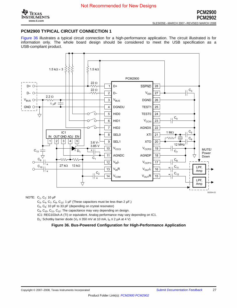
PCM2900 TYPICAL CIRCUIT CONNECTION 1
D+ 28
27
26
25
24
23
22
21
20
19
1
2
3
4
5
6
7
8
9
10
PCM2900
D–
VBUS
DGNDU
HID0
HID1
HID2
SEL0
SEL1
VCCCI
SSPND
XTI
VDDI
DGND
TEST1
TEST0
XTO
VCCP2I
AGNDX
VCCXI
D+
D–
C1
11
12
13
14
AGNDC
V LIN
V RIN
VCOM
18
17
16
15
VCCP1I
V LOUT
V ROUT
AGNDP
22 W
22 W
1.5 k 3W ´ 1.5 kW
GND
VBUS
C2
C9
C10
1 MW
12 MHz
C5
C6
C3
C8
C11
C12
LPF,
Amp
LPF,
Amp
C7
C4
3.6 V–
3.85 V
13 kW27 kW
IN
1
OUT
2
GND
3
ADJ
4
EN
5
IC1
MUTE/
Power
Down
+
+
C13
+
+
+
+
D1
2.2 W
1 Fm
S0264-03
PCM2900PCM2902
SLES035E–MARCH 2007–REVISED MARCH 2008
Figure 36 illustrates a typical circuit connection for a high-performance application. The circuit illustrated is forinformation only. The whole board design should be considered to meet the USB specification as aUSB-compliant product.
NOTE: C1, C2: 10 µFC3, C4, C7, C8, C13: 1 µF (These capacitors must be less than 2 µF.)C5, C6: 10 pF to 33 pF (depending on crystal resonator)C9, C10, C11, C12: The capacitance may vary depending on design.IC1: REG103xA-A (TI) or equivalent. Analog performance may vary depending on IC1.D1: Schottky barrier diode (VF ≤ 350 mV at 10 mA, IR ≤ 2 µA at 4 V)
Figure 36. Bus-Powered Configuration for High-Performance Application
Copyright © 2007–2008, Texas Instruments Incorporated Submit Documentation Feedback 27
Product Folder Link(s): PCM2900 PCM2902
Not Recommended for New Designs
www.ti.com
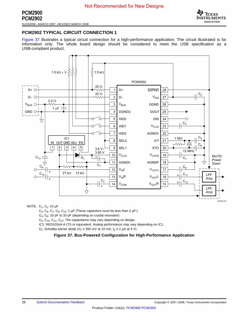
PCM2902 TYPICAL CIRCUIT CONNECTION 1
D+ 28
27
26
25
24
23
22
21
20
19
1
2
3
4
5
6
7
8
9
10
PCM2902
D–
VBUS
DGNDU
HID0
HID1
HID2
SEL0
SEL1
VCCCI
SSPND
XTI
VDDI
DGND
DOUT
DIN
XTO
VCCP2I
AGNDX
VCCXI
D+
D–
C1
11
12
13
14
AGNDC
V LIN
V RIN
VCOM
18
17
16
15
VCCP1I
V LOUT
V ROUT
AGNDP
22 W
22 W
1.5 k 3W ´ 1.5 kW
GND
VBUS
C2
C9
C10
1 MW
12 MHz
C5
C6
C3
C8
C11
C12
LPF,
Amp
LPF,
Amp
C7
C4
3.6 V–
3.85 V
13 kW27 kW
IN
1
OUT
2
GND
3
ADJ
4
EN
5
IC1
MUTE/
Power
Down
+
+
C13
+
+
+
+
D1
2.2 W
1 Fm
S0264-04
PCM2900PCM2902SLES035E–MARCH 2007–REVISED MARCH 2008
Figure 37 illustrates a typical circuit connection for a high-performance application. The circuit illustrated is forinformation only. The whole board design should be considered to meet the USB specification as aUSB-compliant product.
NOTE: C1, C2: 10 µFC3, C4, C7, C8, C13: 1 µF (These capacitors must be less than 2 µF.)C5, C6: 10 pF to 33 pF (depending on crystal resonator)C9, C10, C11, C12: The capacitance may vary depending on design.IC1: REG103xA-A (TI) or equivalent. Analog performance may vary depending on IC1.D1: Schottky barrier diode (VF ≤ 350 mV at 10 mA, IR ≤ 2 µA at 4 V)
Figure 37. Bus-Powered Configuration for High-Performance Application
28 Submit Documentation Feedback Copyright © 2007–2008, Texas Instruments Incorporated
Product Folder Link(s): PCM2900 PCM2902
Not Recommended for New Designs
www.ti.com
PCM2900 TYPICAL CIRCUIT CONNECTION 2
D+ 28
27
26
25
24
23
22
21
20
19
1
2
3
4
5
6
7
8
9
10
PCM2900
D–
VBUS
DGNDU
HID0
HID1
HID2
SEL0
SEL1
VCCCI
SSPND
XTI
VDDI
DGND
TEST1
TEST0
XTO
VCCP2I
AGNDX
VCCXI
D+
D–
C1
11
12
13
14
AGNDC
V LIN
V RIN
VCOM
18
17
16
15
VCCP1I
V LOUT
V ROUT
AGNDP
22 W
22 W
1.5 k 4W ´
GND
VBUS
C2
C9
C10
1 MW
12 MHz
C5
C6
C3
C8
C11
C12
LPF,
Amp
LPF,
Amp
C7
C4
MUTE/
Power
Down
+
+
+
+
+
+
2.2 W
1 Fm
S0265-03
PCM2900PCM2902
SLES035E–MARCH 2007–REVISED MARCH 2008
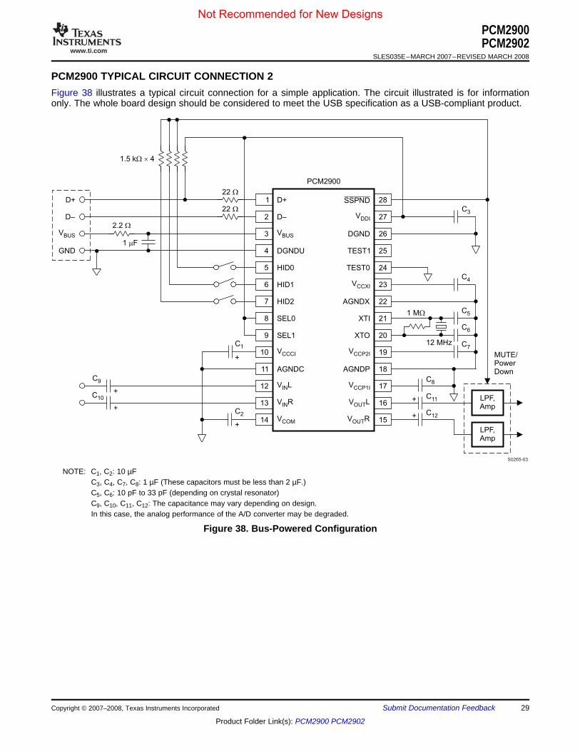
Figure 38 illustrates a typical circuit connection for a simple application. The circuit illustrated is for informationonly. The whole board design should be considered to meet the USB specification as a USB-compliant product.
NOTE: C1, C2: 10 µFC3, C4, C7, C8: 1 µF (These capacitors must be less than 2 µF.)C5, C6: 10 pF to 33 pF (depending on crystal resonator)C9, C10, C11, C12: The capacitance may vary depending on design.In this case, the analog performance of the A/D converter may be degraded.
Figure 38. Bus-Powered Configuration
Copyright © 2007–2008, Texas Instruments Incorporated Submit Documentation Feedback 29
Product Folder Link(s): PCM2900 PCM2902
Not Recommended for New Designs
www.ti.com
PCM2902 TYPICAL CIRCUIT CONNECTION 2
D+ 28
27
26
25
24
23
22
21
20
19
1
2
3
4
5
6
7
8
9
10
PCM2902
D–
VBUS
DGNDU
HID0
HID1
HID2
SEL0
SEL1
VCCCI
SSPND
XTI
VDDI
DGND
DOUT
DIN
XTO
VCCP2I
AGNDX
VCCXI
D+
D–
C1
11
12
13
14
AGNDC
V LIN
V RIN
VCOM
18
17
16
15
VCCP1I
V LOUT
V ROUT
AGNDP
22 W
22 W
1.5 k 4W ´
GND
VBUS
C2
C9
C10
1 MW
12 MHz
C5
C6
C3
C8
C11
C12
LPF,
Amp
LPF,
Amp
C7
C4
MUTE/
Power
Down
+
+
+
+
+
+
2.2 W
1 Fm
S0265-04
PCM2900PCM2902SLES035E–MARCH 2007–REVISED MARCH 2008
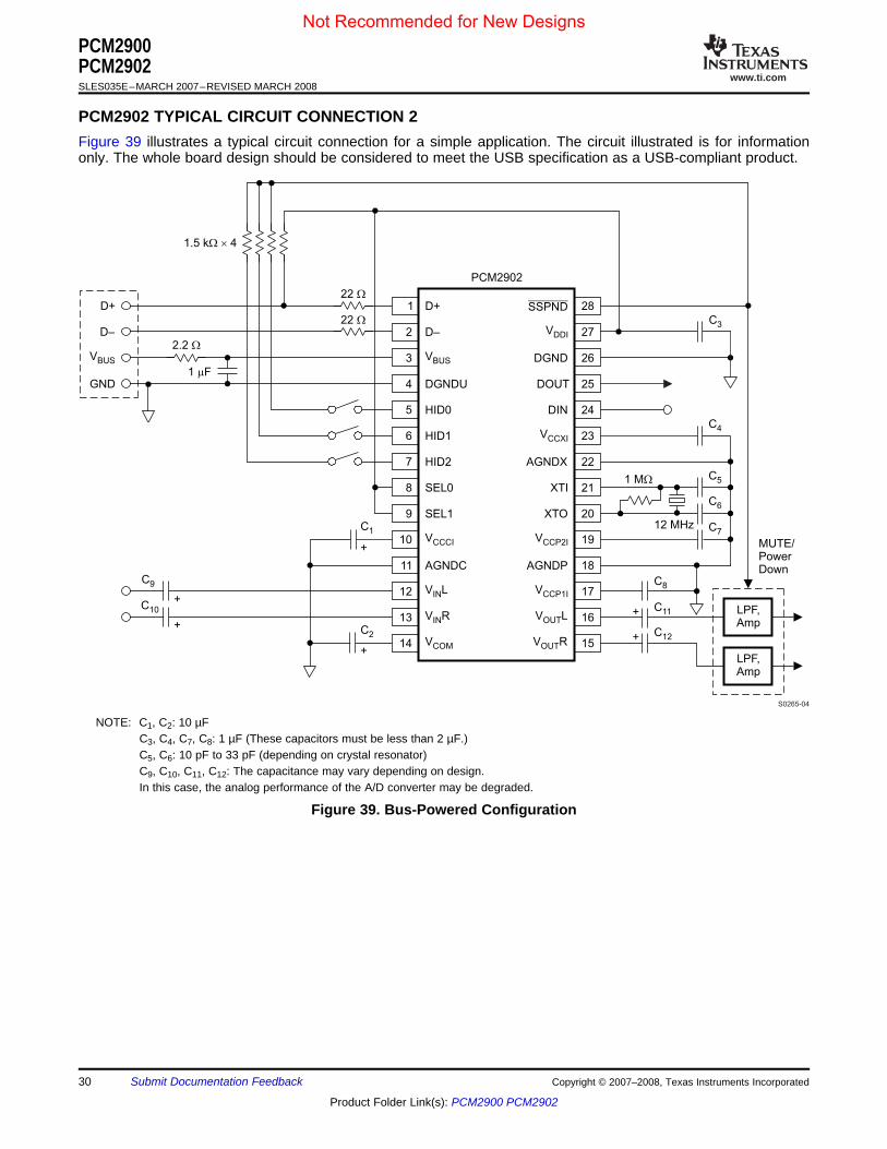
Figure 39 illustrates a typical circuit connection for a simple application. The circuit illustrated is for informationonly. The whole board design should be considered to meet the USB specification as a USB-compliant product.
NOTE: C1, C2: 10 µFC3, C4, C7, C8: 1 µF (These capacitors must be less than 2 µF.)C5, C6: 10 pF to 33 pF (depending on crystal resonator)C9, C10, C11, C12: The capacitance may vary depending on design.In this case, the analog performance of the A/D converter may be degraded.
Figure 39. Bus-Powered Configuration
30 Submit Documentation Feedback Copyright © 2007–2008, Texas Instruments Incorporated
Product Folder Link(s): PCM2900 PCM2902
Not Recommended for New Designs
www.ti.com
APPLICATION INFORMATION
OPERATING ENVIRONMENT
PCM2900PCM2902
SLES035E–MARCH 2007–REVISED MARCH 2008
For current information on the PCM2900/2902 operating environment, see the Updated Operating Environmentsfor PCM270X, PCM290X Applications application report, SLAA374.
xxxxxx
xxxxxx
xxxxxx
xxxxxx
REVISION HISTORY
Changes from Original (March 2002) to Revision A ....................................................................................................... Page
• Changed the status from Product Preview to Production Provided the full data sheet......................................................... 1
Changes from Revision A (May 2002) to Revision B ...................................................................................................... Page
• Changed the description. ....................................................................................................................................................... 1• Changed Interface #2 to include lines 0F, 10, 11, and 12................................................................................................... 22• Added Channel Status Information (PCM2902). ................................................................................................................. 24• Deleted Note: The circuit illustrated above is for information only. The whole board design should be considered to
meet the USB specification as a USB compliant product. From Figure 36, Figure 37, and Figure 38 ............................... 27
Changes from Revision B (June 2004) to Revision C .................................................................................................... Page
• Changed Figure 36, Figure 37, and Figure 38 .................................................................................................................... 27
Changes from Revision C (March 2007) to Revision D .................................................................................................. Page
• Deleted operating environment information from data sheet and added reference to application report ........................... 31
Changes from Revision D (November 2007) to Revision E ........................................................................................... Page
• Changed the Packageing Ordering Information Table to correct the Specified Temperature Range From 25°C to–25°C for the PCM2900 and PCM2902. ............................................................................................................................... 2
Copyright © 2007–2008, Texas Instruments Incorporated Submit Documentation Feedback 31
Product Folder Link(s): PCM2900 PCM2902
Not Recommended for New Designs
PACKAGE OPTION ADDENDUM
www.ti.com 15-Apr-2017
Addendum-Page 1
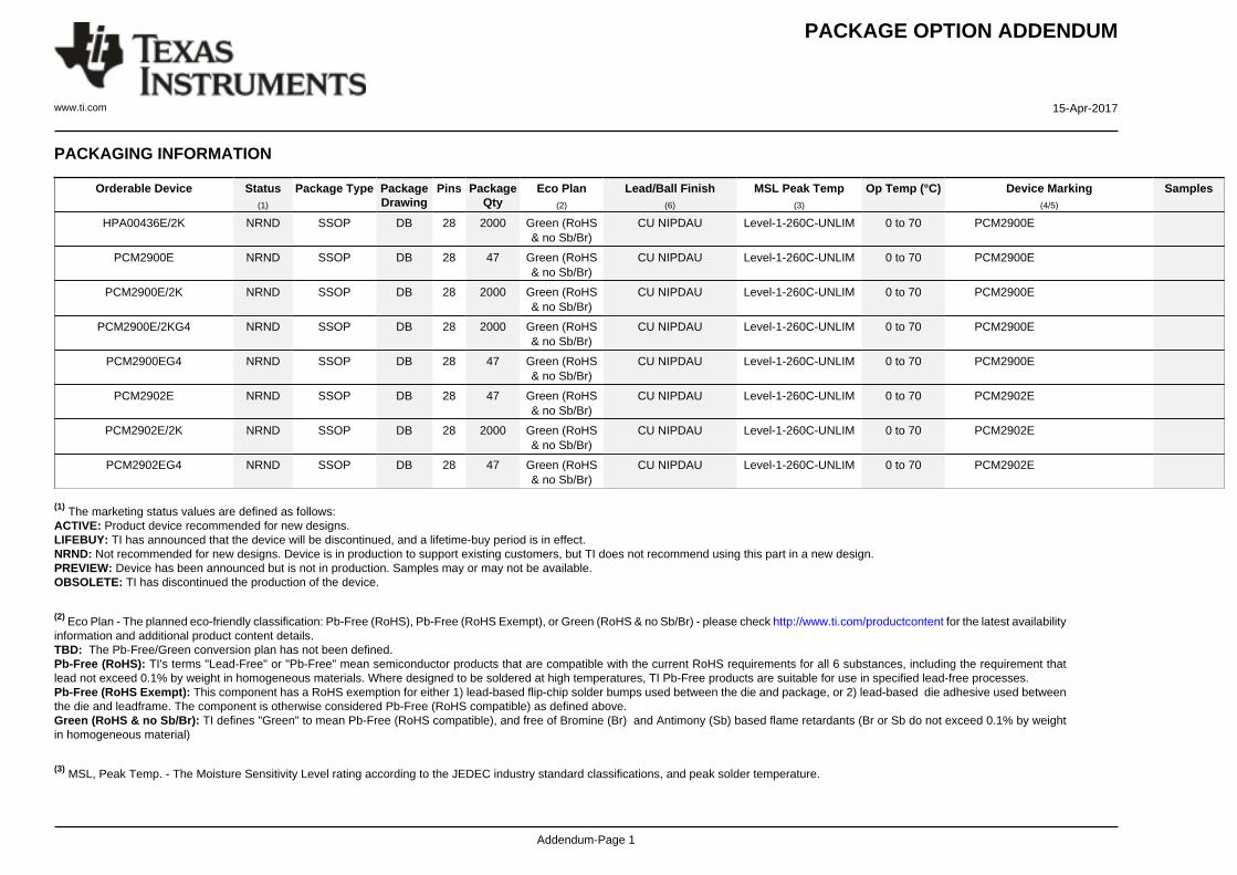
PACKAGING INFORMATION
Orderable Device Status(1)
Package Type PackageDrawing
Pins PackageQty
Eco Plan(2)
Lead/Ball Finish(6)
MSL Peak Temp(3)
Op Temp (°C) Device Marking(4/5)
Samples
HPA00436E/2K NRND SSOP DB 28 2000 Green (RoHS& no Sb/Br)
CU NIPDAU Level-1-260C-UNLIM 0 to 70 PCM2900E
PCM2900E NRND SSOP DB 28 47 Green (RoHS& no Sb/Br)
CU NIPDAU Level-1-260C-UNLIM 0 to 70 PCM2900E
PCM2900E/2K NRND SSOP DB 28 2000 Green (RoHS& no Sb/Br)
CU NIPDAU Level-1-260C-UNLIM 0 to 70 PCM2900E
PCM2900E/2KG4 NRND SSOP DB 28 2000 Green (RoHS& no Sb/Br)
CU NIPDAU Level-1-260C-UNLIM 0 to 70 PCM2900E
PCM2900EG4 NRND SSOP DB 28 47 Green (RoHS& no Sb/Br)
CU NIPDAU Level-1-260C-UNLIM 0 to 70 PCM2900E
PCM2902E NRND SSOP DB 28 47 Green (RoHS& no Sb/Br)
CU NIPDAU Level-1-260C-UNLIM 0 to 70 PCM2902E
PCM2902E/2K NRND SSOP DB 28 2000 Green (RoHS& no Sb/Br)
CU NIPDAU Level-1-260C-UNLIM 0 to 70 PCM2902E
PCM2902EG4 NRND SSOP DB 28 47 Green (RoHS& no Sb/Br)
CU NIPDAU Level-1-260C-UNLIM 0 to 70 PCM2902E
(1) The marketing status values are defined as follows:ACTIVE: Product device recommended for new designs.LIFEBUY: TI has announced that the device will be discontinued, and a lifetime-buy period is in effect.NRND: Not recommended for new designs. Device is in production to support existing customers, but TI does not recommend using this part in a new design.PREVIEW: Device has been announced but is not in production. Samples may or may not be available.OBSOLETE: TI has discontinued the production of the device.
(2) Eco Plan - The planned eco-friendly classification: Pb-Free (RoHS), Pb-Free (RoHS Exempt), or Green (RoHS & no Sb/Br) - please check http://www.ti.com/productcontent for the latest availabilityinformation and additional product content details.TBD: The Pb-Free/Green conversion plan has not been defined.Pb-Free (RoHS): TI's terms "Lead-Free" or "Pb-Free" mean semiconductor products that are compatible with the current RoHS requirements for all 6 substances, including the requirement thatlead not exceed 0.1% by weight in homogeneous materials. Where designed to be soldered at high temperatures, TI Pb-Free products are suitable for use in specified lead-free processes.Pb-Free (RoHS Exempt): This component has a RoHS exemption for either 1) lead-based flip-chip solder bumps used between the die and package, or 2) lead-based die adhesive used betweenthe die and leadframe. The component is otherwise considered Pb-Free (RoHS compatible) as defined above.Green (RoHS & no Sb/Br): TI defines "Green" to mean Pb-Free (RoHS compatible), and free of Bromine (Br) and Antimony (Sb) based flame retardants (Br or Sb do not exceed 0.1% by weightin homogeneous material)
(3) MSL, Peak Temp. - The Moisture Sensitivity Level rating according to the JEDEC industry standard classifications, and peak solder temperature.
PACKAGE OPTION ADDENDUM
www.ti.com 15-Apr-2017
Addendum-Page 2
(4) There may be additional marking, which relates to the logo, the lot trace code information, or the environmental category on the device.
(5) Multiple Device Markings will be inside parentheses. Only one Device Marking contained in parentheses and separated by a "~" will appear on a device. If a line is indented then it is a continuationof the previous line and the two combined represent the entire Device Marking for that device.
(6) Lead/Ball Finish - Orderable Devices may have multiple material finish options. Finish options are separated by a vertical ruled line. Lead/Ball Finish values may wrap to two lines if the finishvalue exceeds the maximum column width.
Important Information and Disclaimer:The information provided on this page represents TI's knowledge and belief as of the date that it is provided. TI bases its knowledge and belief on informationprovided by third parties, and makes no representation or warranty as to the accuracy of such information. Efforts are underway to better integrate information from third parties. TI has taken andcontinues to take reasonable steps to provide representative and accurate information but may not have conducted destructive testing or chemical analysis on incoming materials and chemicals.TI and TI suppliers consider certain information to be proprietary, and thus CAS numbers and other limited information may not be available for release.
In no event shall TI's liability arising out of such information exceed the total purchase price of the TI part(s) at issue in this document sold by TI to Customer on an annual basis.
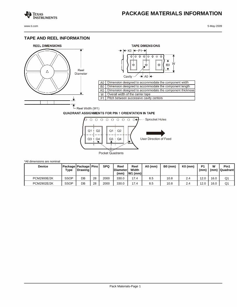
TAPE AND REEL INFORMATION
*All dimensions are nominal
Device PackageType
PackageDrawing
Pins SPQ ReelDiameter
(mm)
ReelWidth
W1 (mm)
A0 (mm) B0 (mm) K0 (mm) P1(mm)
W(mm)
Pin1Quadrant
PCM2900E/2K SSOP DB 28 2000 330.0 17.4 8.5 10.8 2.4 12.0 16.0 Q1
PCM2902E/2K SSOP DB 28 2000 330.0 17.4 8.5 10.8 2.4 12.0 16.0 Q1
PACKAGE MATERIALS INFORMATION
www.ti.com 5-May-2009
Pack Materials-Page 1
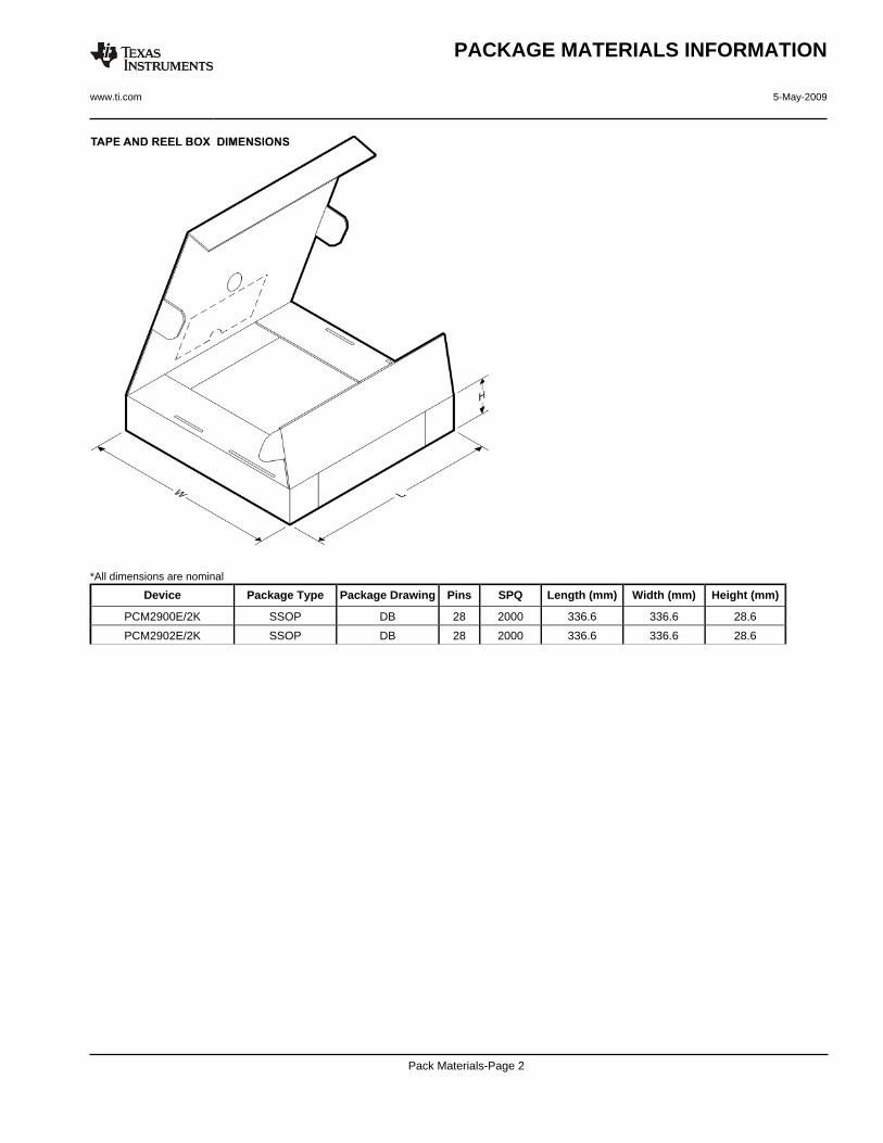
*All dimensions are nominal
Device Package Type Package Drawing Pins SPQ Length (mm) Width (mm) Height (mm)
PCM2900E/2K SSOP DB 28 2000 336.6 336.6 28.6
PCM2902E/2K SSOP DB 28 2000 336.6 336.6 28.6
PACKAGE MATERIALS INFORMATION
www.ti.com 5-May-2009
Pack Materials-Page 2
www.ti.com
PACKAGE OUTLINE
C
26X 0.65
2X8.45
28X 0.380.22
8.27.4 TYP
SEATINGPLANE
0.05 MIN
0.25GAGE PLANE
0 -8
2 MAX
B 5.65.0
NOTE 4
A
10.59.9
NOTE 3
0.950.55
(0.15) TYP
SSOP - 2 mm max heightDB0028ASMALL OUTLINE PACKAGE
4214853/B 03/2018
1
1415
28
0.15 C A B
PIN 1 INDEX AREA
SEE DETAIL A
0.1 C
NOTES: 1. All linear dimensions are in millimeters. Any dimensions in parenthesis are for reference only. Dimensioning and tolerancing per ASME Y14.5M. 2. This drawing is subject to change without notice. 3. This dimension does not include mold flash, protrusions, or gate burrs. Mold flash, protrusions, or gate burrs shall not exceed 0.15 mm per side. 4. This dimension does not include interlead flash. Interlead flash shall not exceed 0.25 mm per side.5. Reference JEDEC registration MO-150.
A 15DETAIL ATYPICAL
SCALE 1.500
www.ti.com
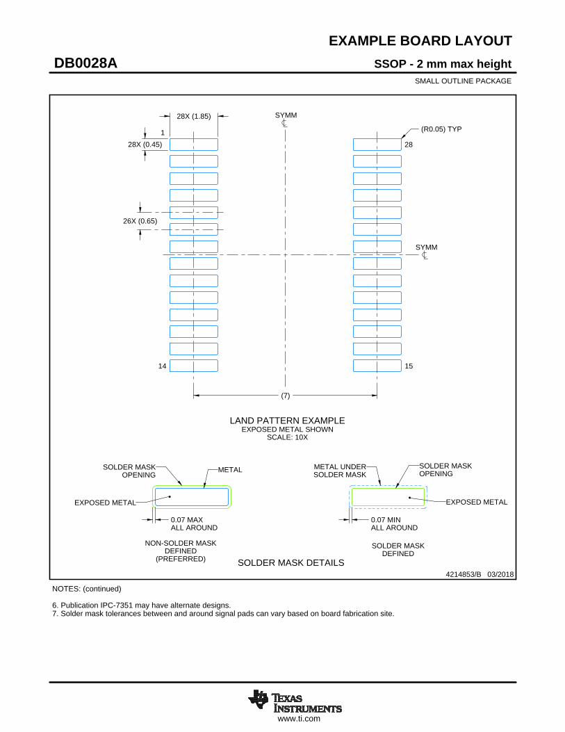
EXAMPLE BOARD LAYOUT
0.07 MAXALL AROUND
0.07 MINALL AROUND
28X (1.85)
28X (0.45)
26X (0.65)
(7)
(R0.05) TYP
SSOP - 2 mm max heightDB0028ASMALL OUTLINE PACKAGE
4214853/B 03/2018
NOTES: (continued) 6. Publication IPC-7351 may have alternate designs. 7. Solder mask tolerances between and around signal pads can vary based on board fabrication site.
LAND PATTERN EXAMPLEEXPOSED METAL SHOWN
SCALE: 10X
SYMM
SYMM
1
14 15
28
15.000
METALSOLDER MASKOPENING
METAL UNDERSOLDER MASK
SOLDER MASKOPENING
EXPOSED METALEXPOSED METAL
SOLDER MASK DETAILS
NON-SOLDER MASKDEFINED
(PREFERRED)
SOLDER MASKDEFINED
www.ti.com
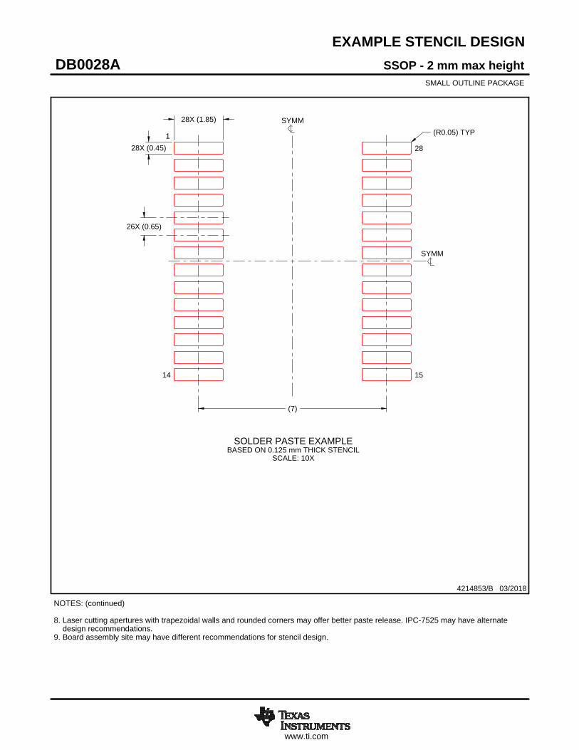
EXAMPLE STENCIL DESIGN
28X (1.85)
28X (0.45)
26X (0.65)
(7)
(R0.05) TYP
SSOP - 2 mm max heightDB0028ASMALL OUTLINE PACKAGE
4214853/B 03/2018
NOTES: (continued) 8. Laser cutting apertures with trapezoidal walls and rounded corners may offer better paste release. IPC-7525 may have alternate design recommendations. 9. Board assembly site may have different recommendations for stencil design.
SOLDER PASTE EXAMPLEBASED ON 0.125 mm THICK STENCIL
SCALE: 10X
SYMM
SYMM
1
14 15
28
IMPORTANT NOTICE
Texas Instruments Incorporated (TI) reserves the right to make corrections, enhancements, improvements and other changes to itssemiconductor products and services per JESD46, latest issue, and to discontinue any product or service per JESD48, latest issue. Buyersshould obtain the latest relevant information before placing orders and should verify that such information is current and complete.TI’s published terms of sale for semiconductor products (http://www.ti.com/sc/docs/stdterms.htm) apply to the sale of packaged integratedcircuit products that TI has qualified and released to market. Additional terms may apply to the use or sale of other types of TI products andservices.Reproduction of significant portions of TI information in TI data sheets is permissible only if reproduction is without alteration and isaccompanied by all associated warranties, conditions, limitations, and notices. TI is not responsible or liable for such reproduceddocumentation. Information of third parties may be subject to additional restrictions. Resale of TI products or services with statementsdifferent from or beyond the parameters stated by TI for that product or service voids all express and any implied warranties for theassociated TI product or service and is an unfair and deceptive business practice. TI is not responsible or liable for any such statements.Buyers and others who are developing systems that incorporate TI products (collectively, “Designers”) understand and agree that Designersremain responsible for using their independent analysis, evaluation and judgment in designing their applications and that Designers havefull and exclusive responsibility to assure the safety of Designers' applications and compliance of their applications (and of all TI productsused in or for Designers’ applications) with all applicable regulations, laws and other applicable requirements. Designer represents that, withrespect to their applications, Designer has all the necessary expertise to create and implement safeguards that (1) anticipate dangerousconsequences of failures, (2) monitor failures and their consequences, and (3) lessen the likelihood of failures that might cause harm andtake appropriate actions. Designer agrees that prior to using or distributing any applications that include TI products, Designer willthoroughly test such applications and the functionality of such TI products as used in such applications.TI’s provision of technical, application or other design advice, quality characterization, reliability data or other services or information,including, but not limited to, reference designs and materials relating to evaluation modules, (collectively, “TI Resources”) are intended toassist designers who are developing applications that incorporate TI products; by downloading, accessing or using TI Resources in anyway, Designer (individually or, if Designer is acting on behalf of a company, Designer’s company) agrees to use any particular TI Resourcesolely for this purpose and subject to the terms of this Notice.TI’s provision of TI Resources does not expand or otherwise alter TI’s applicable published warranties or warranty disclaimers for TIproducts, and no additional obligations or liabilities arise from TI providing such TI Resources. TI reserves the right to make corrections,enhancements, improvements and other changes to its TI Resources. TI has not conducted any testing other than that specificallydescribed in the published documentation for a particular TI Resource.Designer is authorized to use, copy and modify any individual TI Resource only in connection with the development of applications thatinclude the TI product(s) identified in such TI Resource. NO OTHER LICENSE, EXPRESS OR IMPLIED, BY ESTOPPEL OR OTHERWISETO ANY OTHER TI INTELLECTUAL PROPERTY RIGHT, AND NO LICENSE TO ANY TECHNOLOGY OR INTELLECTUAL PROPERTYRIGHT OF TI OR ANY THIRD PARTY IS GRANTED HEREIN, including but not limited to any patent right, copyright, mask work right, orother intellectual property right relating to any combination, machine, or process in which TI products or services are used. Informationregarding or referencing third-party products or services does not constitute a license to use such products or services, or a warranty orendorsement thereof. Use of TI Resources may require a license from a third party under the patents or other intellectual property of thethird party, or a license from TI under the patents or other intellectual property of TI.TI RESOURCES ARE PROVIDED “AS IS” AND WITH ALL FAULTS. TI DISCLAIMS ALL OTHER WARRANTIES ORREPRESENTATIONS, EXPRESS OR IMPLIED, REGARDING RESOURCES OR USE THEREOF, INCLUDING BUT NOT LIMITED TOACCURACY OR COMPLETENESS, TITLE, ANY EPIDEMIC FAILURE WARRANTY AND ANY IMPLIED WARRANTIES OFMERCHANTABILITY, FITNESS FOR A PARTICULAR PURPOSE, AND NON-INFRINGEMENT OF ANY THIRD PARTY INTELLECTUALPROPERTY RIGHTS. TI SHALL NOT BE LIABLE FOR AND SHALL NOT DEFEND OR INDEMNIFY DESIGNER AGAINST ANY CLAIM,INCLUDING BUT NOT LIMITED TO ANY INFRINGEMENT CLAIM THAT RELATES TO OR IS BASED ON ANY COMBINATION OFPRODUCTS EVEN IF DESCRIBED IN TI RESOURCES OR OTHERWISE. IN NO EVENT SHALL TI BE LIABLE FOR ANY ACTUAL,DIRECT, SPECIAL, COLLATERAL, INDIRECT, PUNITIVE, INCIDENTAL, CONSEQUENTIAL OR EXEMPLARY DAMAGES INCONNECTION WITH OR ARISING OUT OF TI RESOURCES OR USE THEREOF, AND REGARDLESS OF WHETHER TI HAS BEENADVISED OF THE POSSIBILITY OF SUCH DAMAGES.Unless TI has explicitly designated an individual product as meeting the requirements of a particular industry standard (e.g., ISO/TS 16949and ISO 26262), TI is not responsible for any failure to meet such industry standard requirements.Where TI specifically promotes products as facilitating functional safety or as compliant with industry functional safety standards, suchproducts are intended to help enable customers to design and create their own applications that meet applicable functional safety standardsand requirements. Using products in an application does not by itself establish any safety features in the application. Designers mustensure compliance with safety-related requirements and standards applicable to their applications. Designer may not use any TI products inlife-critical medical equipment unless authorized officers of the parties have executed a special contract specifically governing such use.Life-critical medical equipment is medical equipment where failure of such equipment would cause serious bodily injury or death (e.g., lifesupport, pacemakers, defibrillators, heart pumps, neurostimulators, and implantables). Such equipment includes, without limitation, allmedical devices identified by the U.S. Food and Drug Administration as Class III devices and equivalent classifications outside the U.S.TI may expressly designate certain products as completing a particular qualification (e.g., Q100, Military Grade, or Enhanced Product).Designers agree that it has the necessary expertise to select the product with the appropriate qualification designation for their applicationsand that proper product selection is at Designers’ own risk. Designers are solely responsible for compliance with all legal and regulatoryrequirements in connection with such selection.Designer will fully indemnify TI and its representatives against any damages, costs, losses, and/or liabilities arising out of Designer’s non-compliance with the terms and provisions of this Notice.
Mailing Address: Texas Instruments, Post Office Box 655303, Dallas, Texas 75265Copyright © 2018, Texas Instruments Incorporated


