
Low Power Stereo Audio CODEC For Portable Audio/Telephony...
102
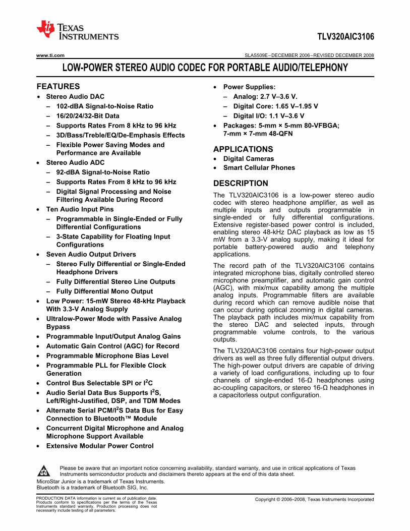
1FEATURES APPLICATIONS DESCRIPTION TLV320AIC3106 www.ti.com........................................................................................................................................ SLAS509E–DECEMBER 2006–REVISED DECEMBER 2008 LOW-POWER STEREO AUDIO CODEC FOR PORTABLE AUDIO/TELEPHONY • Power Supplies: 23• Stereo Audio DAC – Analog: 2.7 V–3.6 V. – 102-dBA Signal-to-Noise Ratio – Digital Core: 1.65 V–1.95 V – 16/20/24/32-Bit Data – Digital I/O: 1.1 V–3.6 V – Supports Rates From 8 kHz to 96 kHz • Packages: 5-mm × 5-mm 80-VFBGA; 7-mm × 7-mm 48-QFN – 3D/Bass/Treble/EQ/De-Emphasis Effects – Flexible Power Saving Modes and Performance are Available • Digital Cameras • Stereo Audio ADC • Smart Cellular Phones – 92-dBA Signal-to-Noise Ratio – Supports Rates From 8 kHz to 96 kHz – Digital Signal Processing and Noise The TLV320AIC3106 is a low-power stereo audio Filtering Available During Record codec with stereo headphone amplifier, as well as • Ten Audio Input Pins multiple inputs and outputs programmable in single-ended or fully differential configurations. – Programmable in Single-Ended or Fully Extensive register-based power control is included, Differential Configurations enabling stereo 48-kHz DAC playback as low as 15 – 3-State Capability for Floating Input mW from a 3.3-V analog supply, making it ideal for Configurations portable battery-powered audio and telephony applications. • Seven Audio Output Drivers – Stereo Fully Differential or Single-Ended The record path of the TLV320AIC3106 contains Headphone Drivers integrated microphone bias, digitally controlled stereo microphone preamplifier, and automatic gain control – Fully Differential Stereo Line Outputs (AGC), with mix/mux capability among the multiple – Fully Differential Mono Output analog inputs. Programmable filters are available • Low Power: 15-mW Stereo 48-kHz Playback during record which can remove audible noise that With 3.3-V Analog Supply can occur during optical zooming in digital cameras. The playback path includes mix/mux capability from • Ultralow-Power Mode with Passive Analog the stereo DAC and selected inputs, through Bypass programmable volume controls, to the various • Programmable Input/Output Analog Gains outputs. • Automatic Gain Control (AGC) for Record The TLV320AIC3106 contains four high-power output • Programmable Microphone Bias Level drivers as well as three fully differential output drivers. • Programmable PLL for Flexible Clock The high-power output drivers are capable of driving a variety of load configurations, including up to four Generation channels of single-ended 16- headphones using • Control Bus Selectable SPI or I 2 C ac-coupling capacitors, or stereo 16- headphones in • Audio Serial Data Bus Supports I 2 S, a capacitorless output configuration. Left/Right-Justified, DSP, and TDM Modes • Alternate Serial PCM/I 2 S Data Bus for Easy Connection to Bluetooth™ Module • Concurrent Digital Microphone and Analog Microphone Support Available • Extensive Modular Power Control 1 Please be aware that an important notice concerning availability, standard warranty, and use in critical applications of Texas Instruments semiconductor products and disclaimers thereto appears at the end of this data sheet. 2MicroStar Junior is a trademark of Texas Instruments. 3Bluetooth is a trademark of Bluetooth SIG, Inc. PRODUCTION DATA information is current as of publication date. Copyright © 2006–2008, Texas Instruments Incorporated Products conform to specifications per the terms of the Texas Instruments standard warranty. Production processing does not necessarily include testing of all parameters.
Transcript of Low Power Stereo Audio CODEC For Portable Audio/Telephony...
1FEATURES
APPLICATIONS
DESCRIPTION
TLV320AIC3106
www.ti.com ........................................................................................................................................ SLAS509E–DECEMBER 2006–REVISED DECEMBER 2008
LOW-POWER STEREO AUDIO CODEC FOR PORTABLE AUDIO/TELEPHONY• Power Supplies:
23• Stereo Audio DAC – Analog: 2.7 V–3.6 V.– 102-dBA Signal-to-Noise Ratio – Digital Core: 1.65 V–1.95 V– 16/20/24/32-Bit Data – Digital I/O: 1.1 V–3.6 V– Supports Rates From 8 kHz to 96 kHz • Packages: 5-mm × 5-mm 80-VFBGA;
7-mm × 7-mm 48-QFN– 3D/Bass/Treble/EQ/De-Emphasis Effects– Flexible Power Saving Modes andPerformance are Available
• Digital Cameras• Stereo Audio ADC• Smart Cellular Phones– 92-dBA Signal-to-Noise Ratio
– Supports Rates From 8 kHz to 96 kHz– Digital Signal Processing and Noise The TLV320AIC3106 is a low-power stereo audioFiltering Available During Record codec with stereo headphone amplifier, as well as
• Ten Audio Input Pins multiple inputs and outputs programmable insingle-ended or fully differential configurations.– Programmable in Single-Ended or FullyExtensive register-based power control is included,Differential Configurationsenabling stereo 48-kHz DAC playback as low as 15– 3-State Capability for Floating Input mW from a 3.3-V analog supply, making it ideal for
Configurations portable battery-powered audio and telephonyapplications.• Seven Audio Output Drivers
– Stereo Fully Differential or Single-Ended The record path of the TLV320AIC3106 containsHeadphone Drivers integrated microphone bias, digitally controlled stereo
microphone preamplifier, and automatic gain control– Fully Differential Stereo Line Outputs(AGC), with mix/mux capability among the multiple– Fully Differential Mono Output analog inputs. Programmable filters are available
• Low Power: 15-mW Stereo 48-kHz Playback during record which can remove audible noise thatWith 3.3-V Analog Supply can occur during optical zooming in digital cameras.
The playback path includes mix/mux capability from• Ultralow-Power Mode with Passive Analogthe stereo DAC and selected inputs, throughBypassprogrammable volume controls, to the various
• Programmable Input/Output Analog Gains outputs.• Automatic Gain Control (AGC) for Record
The TLV320AIC3106 contains four high-power output• Programmable Microphone Bias Level drivers as well as three fully differential output drivers.• Programmable PLL for Flexible Clock The high-power output drivers are capable of driving
a variety of load configurations, including up to fourGenerationchannels of single-ended 16-� headphones using• Control Bus Selectable SPI or I2Cac-coupling capacitors, or stereo 16-� headphones in
• Audio Serial Data Bus Supports I2S, a capacitorless output configuration.Left/Right-Justified, DSP, and TDM Modes
• Alternate Serial PCM/I2S Data Bus for EasyConnection to Bluetooth™ Module
• Concurrent Digital Microphone and AnalogMicrophone Support Available
• Extensive Modular Power Control
1
Please be aware that an important notice concerning availability, standard warranty, and use in critical applications of TexasInstruments semiconductor products and disclaimers thereto appears at the end of this data sheet.
2MicroStar Junior is a trademark of Texas Instruments.3Bluetooth is a trademark of Bluetooth SIG, Inc.
PRODUCTION DATA information is current as of publication date. Copyright © 2006–2008, Texas Instruments IncorporatedProducts conform to specifications per the terms of the TexasInstruments standard warranty. Production processing does notnecessarily include testing of all parameters.
DESCRIPTION (CONTINUED)
TLV320AIC3106
SLAS509E–DECEMBER 2006–REVISED DECEMBER 2008........................................................................................................................................ www.ti.com
These devices have limited built-in ESD protection. The leads should be shorted together or the device placed in conductive foamduring storage or handling to prevent electrostatic damage to the MOS gates.
The stereo audio DAC supports sampling rates from 8 kHz to 96 kHz and includes programmable digital filteringin the DAC path for 3D, bass, treble, midrange effects, speaker equalization, and de-emphasis for 32-kHz,44.1-kHz, and 48-kHz rates. The stereo audio ADC supports sampling rates from 8 kHz to 96 kHz and ispreceded by programmable gain amplifiers or AGC that can provide up to 59.5-dB analog gain for low-levelmicrophone inputs. The TLV320AIC3106 provides an extremely high range of programmability for both attack (8ms–1,408 ms) and for decay (0.05 s–22.4 s). This extended AGC range allows the AGC to be tuned for manytypes of applications.
For battery saving applications where neither analog nor digital signal processing are required, the device can beput in a special analog signal passthru mode. This mode significantly reduces power consumption, as most of thedevice is powered down during this pass through operation.
The serial control bus supports SPI or I2C protocols, while the serial audio data bus is programmable for I2S,left/right-justified, DSP, or TDM modes. A highly programmable PLL is included for flexible clock generation andsupport for all standard audio rates from a wide range of available MCLKs, varying from 512 kHz to 50 MHz, withspecial attention paid to the most popular cases of 12-MHz, 13-MHz, 16-MHz, 19.2-MHz, and 19.68-MHz systemclocks.
The TLV320AIC3106 operates from an analog supply of 2.7 V–3.6 V, a digital core supply of 1.65 V–1.95 V, anda digital I/O supply of 1.1 V–3.6 V. The device is available in the 5-mm × 5-mm, 80-ball MicroStar Junior™ BGApackage and a 7-mm × 7-mm, 48-lead QFN package.
2 Submit Documentation Feedback Copyright © 2006–2008, Texas Instruments Incorporated
Product Folder Link(s): TLV320AIC3106
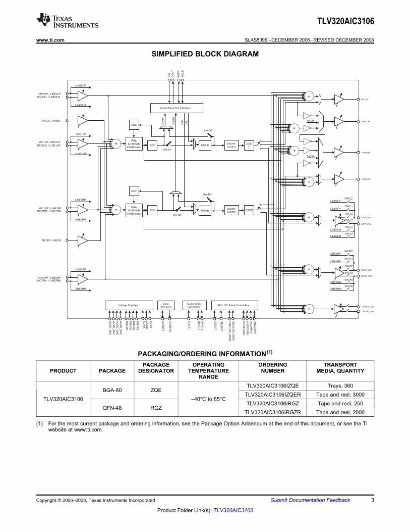
SIMPLIFIED BLOCK DIAGRAM
Audio�Serial�Bus�Interface
MIC3L /�LINE3L
PGA
0/+59.5dB0.5dB�steps
ADC+
+
+
HPRCOM
HPLCOM
HPLOUT
VCM
VCM
DACL
+
Volume
ControlEffects
DIN
DO
UT
BC
LK
WC
LK
DIN
L
DIN
R
DO
UT
L
DO
UT
R
AGC
SW-D2
SW-D1
SPI�/�I2C�Serial�Control�Bus
SE
LE
CT
CS
EL/I2
C_A
DR
0
SC
LK
/I2C
_A
DR
1
MO
SI/G
PIO
MIS
O/G
PIO
Bias/Reference
MIC
BIA
S
SC
L/G
PIO
SD
A/G
PIO
RE
SE
T
MIC
DE
T
Voltage�Supplies
DV
DD
DR
VD
D
DR
VD
D
DR
VS
S
DR
VS
S
DV
SS
IOV
DD
AV
DD
_A
DC
AV
SS
_A
DC
AV
DD
_D
AC
AV
SS
_D
AC
Audio�ClockGeneration
MC
LK
GP
IO_1
GP
IO_2
+
+
+
HPROUT
MIC3R�/�LINE3R
ADCPGA
0/+59.5dB
0.5dB�steps
+ DACRVolumeControlEffects
AGC
SW-D3
SW-D4
+MONO_LOP
MONO_LOM
LINE1RP
LINE2RM
LINE2RP
LINE1RM
SW-R0
SW-R3
SW-R1
SW-R2
SW-R4
SW-R5
RIGHT_LOP
RIGHT_LOM
LINE1LP
LINE2LM
LINE2LP
LINE1LM
SW-L0
SW-L3
SW-L1
SW-L2
SW-L4
SW-L5
LEFT_LOP
LEFT_LOM
MIC2RM��/�LINE2RMMIC2RP /�LINE2RP
LINE2RP
LINE2RM
MIC1RM��/�LINE1RMMIC1RP /�LINE1RP
LINE1RP
LINE1RM
MIC2LM��/�LINE2LMMIC2LP /�LINE2LP
LINE2LP
LINE2LM
MIC1LM��/�LINE1LM
MIC1LP /�LINE1LP
LINE1LP
LINE1LM
TLV320AIC3106
www.ti.com ........................................................................................................................................ SLAS509E–DECEMBER 2006–REVISED DECEMBER 2008
PACKAGING/ORDERING INFORMATION(1)
PACKAGE OPERATING ORDERING TRANSPORTPRODUCT PACKAGE DESIGNATOR TEMPERATURE NUMBER MEDIA, QUANTITY
RANGETLV320AIC3106IZQE Trays, 360
BGA-80 ZQETLV320AIC3106IZQER Tape and reel, 3000
TLV320AIC3106 –40°C to 85°CTLV320AIC3106IRGZ Tape and reel, 250
QFN-48 RGZTLV320AIC3106IRGZR Tape and reel, 2000
(1) For the most current package and ordering information, see the Package Option Addendum at the end of this document, or see the TIwebsite at www.ti.com.
Copyright © 2006–2008, Texas Instruments Incorporated Submit Documentation Feedback 3
Product Folder Link(s): TLV320AIC3106
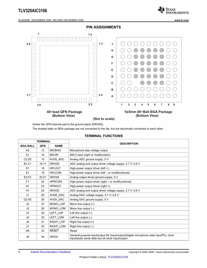
PIN ASSIGNMENTS
A
1 2 3 4 5 6 7 8 9
B
C
D
E
F
G
H
J
48!lead�QFN�Package(Bottom�View)
5x5mm�80!Ball�BGA Package(Bottom�View)
4�8
1 1�2
1�3
2�4
2�53�6
3�7
(Not�to�scale)
TLV320AIC3106
SLAS509E–DECEMBER 2006–REVISED DECEMBER 2008........................................................................................................................................ www.ti.com
Solder the QFN thermal pad to the ground plane (DRVSS).The shaded balls on BGA package are not connected to the die, but are electrically connected to each other.
TERMINAL FUNCTIONSTERMINAL
DESCRIPTIONBGA BALL QFN NAME
A2 13 MICBIAS Microphone bias voltage outputA1 14 MIC3R MIC3 input (right or multifunction)
C2,D2 15 AVSS_ADC Analog ADC ground supply, 0 VB1,C1 16,17 DRVDD ADC analog and output driver voltage supply, 2.7 V–3.6 VD1 18 HPLOUT High-power output driver (left +)E1 19 HPLCOM High-power output driver (left – or multifunctional)E2,F2 20,21 DRVSS Analog output driver ground supply, 0 VF1 22 HPRCOM High-power output driver (right – or multifunctional)G1 23 HPROUT High-power output driver (right +)H1 24 DRVDD ADC analog and output driver voltage supply, 2.7 V–3.6 VJ1 25 AVDD_DAC Analog DAC voltage supply, 2.7 V–3.6 V
G2,H2 26 AVSS_DAC Analog DAC ground supply, 0 VJ2 27 MONO_LOP Mono line output (+)J3 28 MONO_LOM Mono line output (–)J4 29 LEFT_LOP Left line output (+)J5 30 LEFT_LOM Left line output (–)J6 31 RIGHT_LOP Right line output (+)J7 32 RIGHT_LOM Right line output (–)H8 33 RESET Reset
General-purpose input/output #2 (input/output)/digital microphone data input/PLL clockJ8 34 GPIO2 input/audio serial data bus bit clock input/output
4 Submit Documentation Feedback Copyright © 2006–2008, Texas Instruments Incorporated
Product Folder Link(s): TLV320AIC3106
TLV320AIC3106
www.ti.com ........................................................................................................................................ SLAS509E–DECEMBER 2006–REVISED DECEMBER 2008
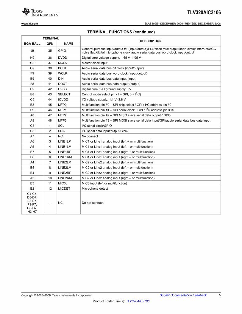
TERMINAL FUNCTIONS (continued)TERMINAL
DESCRIPTIONBGA BALL QFN NAME
General-purpose input/output #1 (input/output)/PLL/clock mux output/short circuit interrupt/AGCJ9 35 GPIO1 noise flag/digital microphone clock audio serial data bus word clock input/outputH9 36 DVDD Digital core voltage supply, 1.65 V–1.95 VG8 37 MCLK Master clock inputG9 38 BCLK Audio serial data bus bit clock (input/output)F9 39 WCLK Audio serial data bus word clock (input/output)E9 40 DIN Audio serial data bus data input (input)F8 41 DOUT Audio serial data bus data output (output)D9 42 DVSS Digital core / I/O ground supply, 0VE8 43 SELECT Control mode select pin (1 = SPI, 0 = I2C)C9 44 IOVDD I/O voltage supply, 1.1 V–3.6 VB8 45 MFP0 Multifunction pin #0 – SPI chip select / GPI / I2C address pin #0B9 46 MFP1 Multifunction pin #1 – SPI serial clock / GPI / I2C address pin #1SA8 47 MFP2 Multifunction pin #2 – SPI MISO slave serial data output / GPOIA9 48 MFP3 Multifunction pin #3 – SPI MOSI slave serial data input/GPI/audio serial data bus data inputC8 1 SCL I2C serial clock/GPIOD8 2 SDA I2C serial data input/output/GPIOA7 – NC No connectA6 3 LINE1LP MIC1 or Line1 analog input (left + or multifunction)A5 4 LINE1LM MIC1 or Line1 analog input (left – or multifunction)B7 5 LINE1RP MIC1 or Line1 analog input (right + or multifunction)B6 6 LINE1RM MIC1 or Line1 analog input (right – or multifunction)A4 7 LINE2LP MIC2 or Line2 analog input (left + or multifunction)B5 8 LINE2LM MIC2 or Line2 analog input (left – or multifunction)B4 9 LINE2RP MIC2 or Line2 analog input (right + or multifunction)A3 10 LINE2RM MIC2 or Line2 analog input (right – or multifunction)B3 11 MIC3L MIC3 input (left or multifunction)B2 12 MICDET Microphone detect
C4-C7,D3-D7,E3-E7, – NC Do not connect.F3-F7,G3-G7,H3-H7
Copyright © 2006–2008, Texas Instruments Incorporated Submit Documentation Feedback 5
Product Folder Link(s): TLV320AIC3106
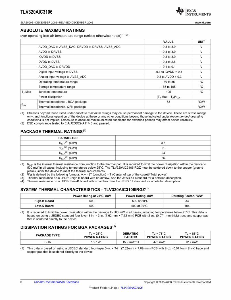
ABSOLUTE MAXIMUM RATINGS
PACKAGE THERMAL RATINGS(1)
SYSTEM THERMAL CHARACTERISTICS - TLV320AIC3106IRGZ(1)
DISSIPATION RATINGS FOR BGA PACKAGES(1)
TLV320AIC3106
SLAS509E–DECEMBER 2006–REVISED DECEMBER 2008........................................................................................................................................ www.ti.com
over operating free-air temperature range (unless otherwise noted)(1) (2)
VALUE UNITAVDD_DAC to AVSS_DAC, DRVDD to DRVSS, AVSS_ADC –0.3 to 3.9 VAVDD to DRVSS –0.3 to 3.9 VIOVDD to DVSS –0.3 to 3.9 VDVDD to DVSS –0.3 to 2.5 VAVDD_DAC to DRVDD –0.1 to 0.1 VDigital input voltage to DVSS –0.3 to IOVDD + 0.3 VAnalog input voltage to AVSS_ADC –0.3 to AVDD + 0.3 VOperating temperature range –40 to 85 °CStorage temperature range –65 to 105 °C
TJ Max Junction temperature 105 °CPower dissipation (TJ Max – TA)/θJAThermal impedance , BGA package 63 °C/W
θJA Thermal impedance, QFN package — °C/W
(1) Stresses beyond those listed under absolute maximum ratings may cause permanent damage to the device. These are stress ratingsonly, and functional operation of the device at these or any other conditions beyond those indicated under recommended operatingconditions is not implied. Exposure to absolute-maximum-rated conditions for extended periods may affect device reliability.
(2) ESD complicance tested to EIA/JESD22-A114-B and passed.
PARAMETERRθJP
(1) (C/W) 3.5ȌJT(2) (°C/W) 2RθJA
(3) (C/W) 24RθJA
(4) (C/W) 85
(1) RθJP is the internal thermal resistance from junction to the thermal pad. It is required to limit the power dissipation within the device to500 mW in all cases, including temperatures below 25°C. The TLV320AIC3106IRGZ must be soldered down to the copper (groundplane) under the device to meet the thermal requirements.
(2) ȌJT is defined by the following formula: ȌJT = [T (Junction) – T (Center of top of the case)]/(Total power)(3) Thermal resistance on a JEDEC high-K board with no airflow. See the JESD 51 standard for a detailed description.(4) Thermal resistance on a JEDEC low-K board with no airflow. See the JESD 51 standard for a detailed description.
Power Rating at 25°C, mW Power Rating, mW Derating Factor, °C/WHigh-K Board 500 500 at 80°C 33Low-K Board 500 500 at 30°C 104
(1) It is required to limit the power dissipation within the package to 500 mW in all cases, including temperatures below 25°C. This data isbased on using a JEDEC standard four-layer 3-in. × 3-in. (7.62-mm × 7.62-mm) PCB with 2-oz. (0.071-mm thick) trace and copper padthat is soldered directly to the device.
TA = 25°C DERATING TA = 75°C TA = 85°CPACKAGE TYPE POWER RATING FACTOR POWER RATING POWER RATINGBGA 1.27 W 15.9 mW/°C 476 mW 317 mW
(1) This data is based on using a JEDEC standard four-layer 3-in. × 3-in. (7.62-mm × 7.62-mm) PCB with 2-oz. (0.071-mm thick) trace andcopper pad that is soldered directly to the device.
6 Submit Documentation Feedback Copyright © 2006–2008, Texas Instruments Incorporated
Product Folder Link(s): TLV320AIC3106

RECOMMENDED OPERATING CONDITIONS
TLV320AIC3106
www.ti.com ........................................................................................................................................ SLAS509E–DECEMBER 2006–REVISED DECEMBER 2008
over operating free-air temperature range (unless otherwise noted)
MIN NOM MAX UNITAVDD_DAC, DRVDD(1) Analog supply voltage 2.7 3.3 3.6 VDVDD(1) Digital core supply voltage 1.65 1.8 1.95 VIOVDD(1) Digital I/O supply voltage 1.1 1.8 3.6 VVI Analog full-scale 0-dB input voltage (DRVDD1 = 3.3 V) 0.707 VRMS
Stereo line output load resistance 10 k�Stereo headphone output load resistance 16 �Digital output load capacitance 10 pF
TA Operating free-air temperature –40 85 °C
(1) Analog voltage values are with respect to AVSS_ADC, AVSS_DAC, DRVSS; digital voltage values are with respect to DVSS.
Copyright © 2006–2008, Texas Instruments Incorporated Submit Documentation Feedback 7
Product Folder Link(s): TLV320AIC3106

ELECTRICAL CHARACTERISTICS
TLV320AIC3106
SLAS509E–DECEMBER 2006–REVISED DECEMBER 2008........................................................................................................................................ www.ti.com
At 25°C, AVDD_DAC, DRVDD, IOVDD = 3.3 V, DVDD = 1.8 V, fS = 48-kHz, 16-bit audio data (unless otherwise noted)PARAMETER TEST CONDITIONS MIN TYP MAX UNIT
AUDIO ADC
Input signal level (0-dB) Single-ended input 0.707 VRMSSignal-to-noise ratio, fS = 48 ksps, 0-dB PGA gain, inputs ac-shorted to ground 80 92 dBA-weighted(1) (2)
Dynamic range (2) fS = 48 ksps, 0-dB PGA gain, –60 dB full-scale input signal 91 dB
fS = 48 ksps, 0-dB PGA gain, –2dB full-scale, 1-kHz inputTHD Total harmonic distortion –88 –70 dBsignal
217-Hz signal applied to DRVDD 49PSRR Power supply rejection ratio dB
1-kHz signal applied to DRVDD 46
fS = 48 ksps, 0-dB PGA gain, –2dB full-scale, 1-kHz inputGain error 0.84 dBsignal
1-kHz, –2-dB full-scale signal, MIC3L to MIC3R –86
Input channel separation 1-kHz, –2-dB full-scale signal, MIC2L to MIC2R –98 dB
1-kHz, –2-dB full-scale signal, MIC1L to MIC1R –75
ADC programmable gain amplifier 1-kHz input tone 59.5 dBmaximum gain
ADC programmable gain amplifier 0.5 dBstep size
MIC1L/MIC1R inputs routed to single ADC 20Input mix attenuation = 0 dB
MIC1L/MIC1R inputs routed to single ADC, input mix 80attenuation = 12 dB
MIC2L/MIC2R inputs routed to single ADC 20Input mix attenuation = 0 dBInput resistance k�
MIC2L/MIC2R inputs routed to single ADC, input mix 80attenuation = 12 dB
MIC3L/MIC3R inputs routed to single ADC 20Input mix attenuation = 0 dB
MIC3L/MIC3R inputs routed to single ADC, input mix 80attenuation = 12 dB
Input level control minimum 0 dBattenuation setting
Input level control maximum 12 dBattenuation setting
Input signal level Differential Input 1.414 VRMSSignal-to-noise ratio, fS = 48 ksps, 0-dB PGA gain, inputs ac-shorted to ground, 92 dBA-weighted(1) (2) differential mode
fS = 48 ksps, 0-dB PGA gain, –2-dB full-scale 1-kHz inputTHD Total harmonic distortion –91 dBsignal, differential mode
ANALOG PASS THROUGH MODE
MIC1/LINE1 to LINE_OUT 330Input to output switch resistance, �(rdsON) MIC2/LINE2 to LINE_OUT 330
ADC DIGITAL DECIMATION FILTER, fS = 48 kHz
Filter gain from 0 to 0.39 fS ±0.1 dB
Filter gain at 0.4125 fS –0.25 dB
Filter gain at 0.45 fS –3 dB
Filter gain at 0.5 fS –17.5 dB
Filter gain from 0.55 fS to 64 fS –75 dB
Filter group delay 17/fS s
(1) Ratio of output level with 1-kHz full-scale sine-wave input, to the output level with the inputs short circuited, measured A-weighted over a20-Hz to 20-kHz bandwidth using an audio analyzer.
(2) All performance measurements done with 20-kHz low-pass filter and, where noted, A-weighted filter. Failure to use such a filter mayresult in higher THD+N and lower SNR and dynamic range readings than shown in the Electrical Characteristics. The low-pass filterremoves out-of-band noise, which, although not audible, may affect dynamic specification values.
8 Submit Documentation Feedback Copyright © 2006–2008, Texas Instruments Incorporated
Product Folder Link(s): TLV320AIC3106
TLV320AIC3106
www.ti.com ........................................................................................................................................ SLAS509E–DECEMBER 2006–REVISED DECEMBER 2008
ELECTRICAL CHARACTERISTICS (continued)At 25°C, AVDD_DAC, DRVDD, IOVDD = 3.3 V, DVDD = 1.8 V, fS = 48-kHz, 16-bit audio data (unless otherwise noted)
PARAMETER TEST CONDITIONS MIN TYP MAX UNIT
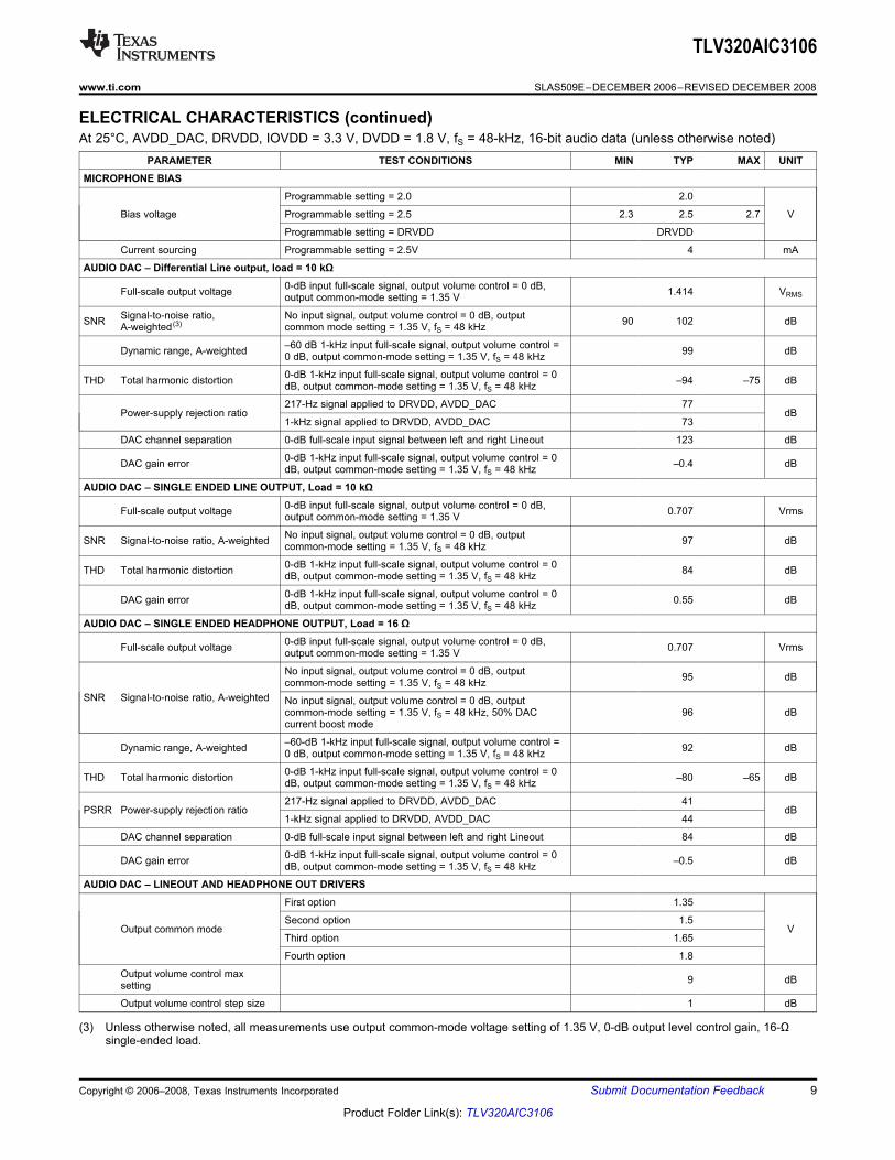
MICROPHONE BIAS
Programmable setting = 2.0 2.0
Bias voltage Programmable setting = 2.5 2.3 2.5 2.7 V
Programmable setting = DRVDD DRVDD
Current sourcing Programmable setting = 2.5V 4 mA
AUDIO DAC – Differential Line output, load = 10 k�
0-dB input full-scale signal, output volume control = 0 dB,Full-scale output voltage 1.414 VRMSoutput common-mode setting = 1.35 V
Signal-to-noise ratio, No input signal, output volume control = 0 dB, outputSNR 90 102 dBA-weighted(3) common mode setting = 1.35 V, fS = 48 kHz
–60 dB 1-kHz input full-scale signal, output volume control =Dynamic range, A-weighted 99 dB0 dB, output common-mode setting = 1.35 V, fS = 48 kHz
0-dB 1-kHz input full-scale signal, output volume control = 0THD Total harmonic distortion –94 –75 dBdB, output common-mode setting = 1.35 V, fS = 48 kHz
217-Hz signal applied to DRVDD, AVDD_DAC 77Power-supply rejection ratio dB
1-kHz signal applied to DRVDD, AVDD_DAC 73
DAC channel separation 0-dB full-scale input signal between left and right Lineout 123 dB
0-dB 1-kHz input full-scale signal, output volume control = 0DAC gain error –0.4 dBdB, output common-mode setting = 1.35 V, fS = 48 kHz
AUDIO DAC – SINGLE ENDED LINE OUTPUT, Load = 10 k�
0-dB input full-scale signal, output volume control = 0 dB,Full-scale output voltage 0.707 Vrmsoutput common-mode setting = 1.35 V
No input signal, output volume control = 0 dB, outputSNR Signal-to-noise ratio, A-weighted 97 dBcommon-mode setting = 1.35 V, fS = 48 kHz
0-dB 1-kHz input full-scale signal, output volume control = 0THD Total harmonic distortion 84 dBdB, output common-mode setting = 1.35 V, fS = 48 kHz
0-dB 1-kHz input full-scale signal, output volume control = 0DAC gain error 0.55 dBdB, output common-mode setting = 1.35 V, fS = 48 kHz
AUDIO DAC – SINGLE ENDED HEADPHONE OUTPUT, Load = 16 �
0-dB input full-scale signal, output volume control = 0 dB,Full-scale output voltage 0.707 Vrmsoutput common-mode setting = 1.35 V
No input signal, output volume control = 0 dB, output 95 dBcommon-mode setting = 1.35 V, fS = 48 kHzSNR Signal-to-noise ratio, A-weighted No input signal, output volume control = 0 dB, output
common-mode setting = 1.35 V, fS = 48 kHz, 50% DAC 96 dBcurrent boost mode
–60-dB 1-kHz input full-scale signal, output volume control =Dynamic range, A-weighted 92 dB0 dB, output common-mode setting = 1.35 V, fS = 48 kHz
0-dB 1-kHz input full-scale signal, output volume control = 0THD Total harmonic distortion –80 –65 dBdB, output common-mode setting = 1.35 V, fS = 48 kHz
217-Hz signal applied to DRVDD, AVDD_DAC 41PSRR Power-supply rejection ratio dB
1-kHz signal applied to DRVDD, AVDD_DAC 44
DAC channel separation 0-dB full-scale input signal between left and right Lineout 84 dB
0-dB 1-kHz input full-scale signal, output volume control = 0DAC gain error –0.5 dBdB, output common-mode setting = 1.35 V, fS = 48 kHz
AUDIO DAC – LINEOUT AND HEADPHONE OUT DRIVERS
First option 1.35
Second option 1.5Output common mode V
Third option 1.65
Fourth option 1.8
Output volume control max 9 dBsetting
Output volume control step size 1 dB
(3) Unless otherwise noted, all measurements use output common-mode voltage setting of 1.35 V, 0-dB output level control gain, 16-�single-ended load.
Copyright © 2006–2008, Texas Instruments Incorporated Submit Documentation Feedback 9
Product Folder Link(s): TLV320AIC3106

TLV320AIC3106
SLAS509E–DECEMBER 2006–REVISED DECEMBER 2008........................................................................................................................................ www.ti.com
ELECTRICAL CHARACTERISTICS (continued)At 25°C, AVDD_DAC, DRVDD, IOVDD = 3.3 V, DVDD = 1.8 V, fS = 48-kHz, 16-bit audio data (unless otherwise noted)
PARAMETER TEST CONDITIONS MIN TYP MAX UNIT
DAC DIGITAL INTERPOLATION – FILTER fS = 48 ksps
Pass band 0 0.45 fS Hz
Pass-band ripple ±0.06 dB
Transition band 0.45 fS 0.55 fS Hz
Stop band 0.55 fS 7.5 fS Hz
Stop-band attenuation 65 dB
Group delay 21/fS s
DIGITAL I/O
0.3 ×VIL Input low level –0.3 VIOVDD
0.7 ×IOVDD > 1.6 V IOVDDVIH Input high level(4) VIOVDD < 1.6 V 1.1
0.1 ×VOL Output low level VIOVDD
0.8 ×VOH Output high level VIOVDD
POWER CONSUMPTION, DRVDD, AVDD_DAC = 3.3 V, DVDD = 1.8 V, IOVDD = 3.3 V
IDRVDD+IAVDD_DAC 0.1RESET held low µA
IDVDD 0.2
IDRVDD+IAVDD_DAC 2.1Mono ADC record, fS = 8 ksps, mAI2S slave, AGC off, no signalIDVDD 0.5
IDRVDD+IAVDD_DAC 4.1Stereo ADC record, fS = 8 ksps, mAI2S slave, AGC off, no signalIDVDD 0.6
IDRVDD+IAVDD_DAC 4.3Stereo ADC record, fS = 48 ksps, mAI2S slave, AGC off, no signalIDVDD 2.5
IDRVDD+IAVDD_DAC Stereo DAC playback to Lineout, 3.5analog mixer bypassed, fS = 48 mA
IDVDD 2.3ksps, I2S slave
IDRVDD+IAVDD_DAC 4.9Stereo DAC playback to Lineout, mAfS = 48 ksps, I2S slave, no signalIDVDD 2.3
IDRVDD+IAVDD_DAC Stereo DAC playback to stereo 6.7single-ended headphone, fS = 48 mA
IDVDD 2.3ksps, I2S slave, no signal
IDRVDD+IAVDD_DAC 3.1Stereo Linein to stereo Lineout, mAno signalIDVDD 0
IDRVDD+IAVDD_DAC 1.4Extra power when PLL enabled mA
IDVDD 0.9
IDRVDD+IAVDD_DAC 28All blocks powered down, µAheadset detedtion enabledIDVDD 2
(4) When IOVDD < 1.6V, minimum VIH is 1.1 V.
10 Submit Documentation Feedback Copyright © 2006–2008, Texas Instruments Incorporated
Product Folder Link(s): TLV320AIC3106
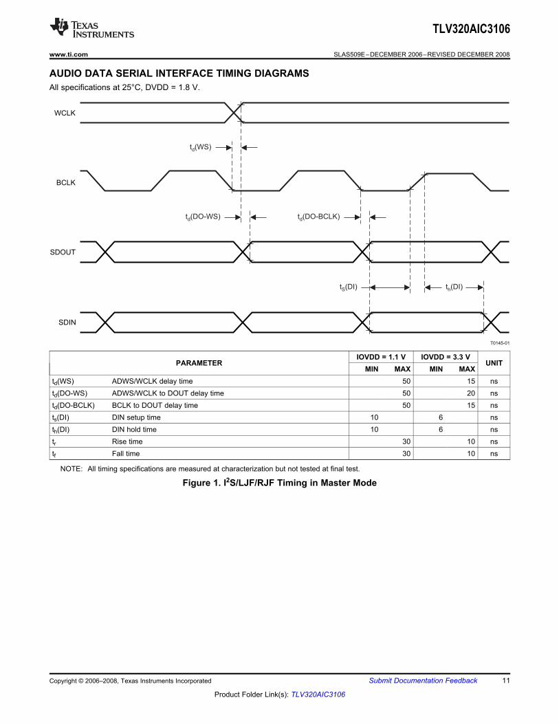
AUDIO DATA SERIAL INTERFACE TIMING DIAGRAMS
T0145-01
WCLK
BCLK
SDOUT
SDIN
t (DO-BCLK)dt (DO-WS)d
t (WS)d
t (DI)S t (DI)h
TLV320AIC3106
www.ti.com ........................................................................................................................................ SLAS509E–DECEMBER 2006–REVISED DECEMBER 2008
All specifications at 25°C, DVDD = 1.8 V.
IOVDD = 1.1 V IOVDD = 3.3 VPARAMETER UNIT
MIN MAX MIN MAXtd(WS) ADWS/WCLK delay time 50 15 nstd(DO-WS) ADWS/WCLK to DOUT delay time 50 20 nstd(DO-BCLK) BCLK to DOUT delay time 50 15 nsts(DI) DIN setup time 10 6 nsth(DI) DIN hold time 10 6 nstr Rise time 30 10 nstf Fall time 30 10 ns
NOTE: All timing specifications are measured at characterization but not tested at final test.
Figure 1. I2S/LJF/RJF Timing in Master Mode
Copyright © 2006–2008, Texas Instruments Incorporated Submit Documentation Feedback 11
Product Folder Link(s): TLV320AIC3106
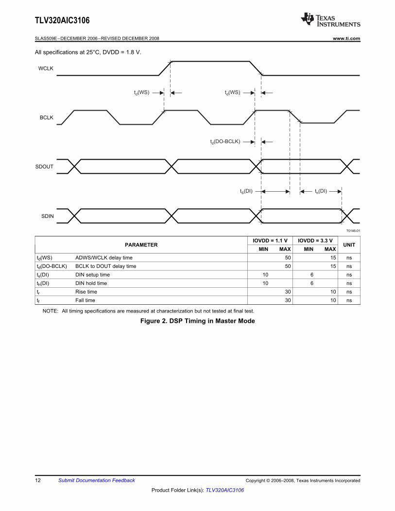
T0146-01
WCLK
BCLK
SDOUT
SDIN
t (DO-BCLK)d
t (WS)d t (WS)d
t (DI)S t (DI)h
TLV320AIC3106
SLAS509E–DECEMBER 2006–REVISED DECEMBER 2008........................................................................................................................................ www.ti.com
All specifications at 25°C, DVDD = 1.8 V.
IOVDD = 1.1 V IOVDD = 3.3 VPARAMETER UNIT
MIN MAX MIN MAXtd(WS) ADWS/WCLK delay time 50 15 nstd(DO-BCLK) BCLK to DOUT delay time 50 15 nsts(DI) DIN setup time 10 6 nsth(DI) DIN hold time 10 6 nstr Rise time 30 10 nstf Fall time 30 10 ns
NOTE: All timing specifications are measured at characterization but not tested at final test.
Figure 2. DSP Timing in Master Mode
12 Submit Documentation Feedback Copyright © 2006–2008, Texas Instruments Incorporated
Product Folder Link(s): TLV320AIC3106
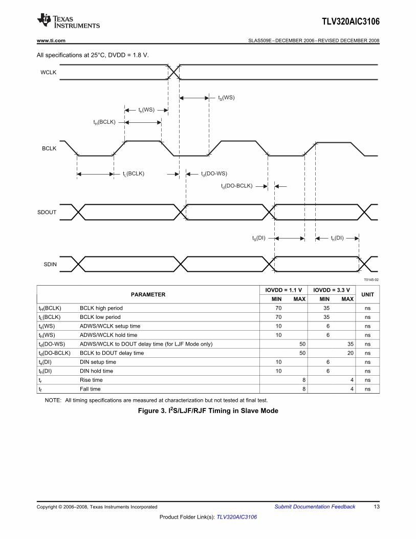
T0145-02
WCLK
BCLK
SDOUT
SDIN
t (WS)h
t (BCLK)H
t (DO-BCLK)d
t (DO-WS)d
t (DI)S
t (BCLK)L
t (DI)h
t (WS)S
TLV320AIC3106
www.ti.com ........................................................................................................................................ SLAS509E–DECEMBER 2006–REVISED DECEMBER 2008
All specifications at 25°C, DVDD = 1.8 V.
IOVDD = 1.1 V IOVDD = 3.3 VPARAMETER UNIT
MIN MAX MIN MAXtH(BCLK) BCLK high period 70 35 nstL(BCLK) BCLK low period 70 35 nsts(WS) ADWS/WCLK setup time 10 6 nsth(WS) ADWS/WCLK hold time 10 6 nstd(DO-WS) ADWS/WCLK to DOUT delay time (for LJF Mode only) 50 35 nstd(DO-BCLK) BCLK to DOUT delay time 50 20 nsts(DI) DIN setup time 10 6 nsth(DI) DIN hold time 10 6 nstr Rise time 8 4 nstf Fall time 8 4 ns
NOTE: All timing specifications are measured at characterization but not tested at final test.
Figure 3. I2S/LJF/RJF Timing in Slave Mode
Copyright © 2006–2008, Texas Instruments Incorporated Submit Documentation Feedback 13
Product Folder Link(s): TLV320AIC3106
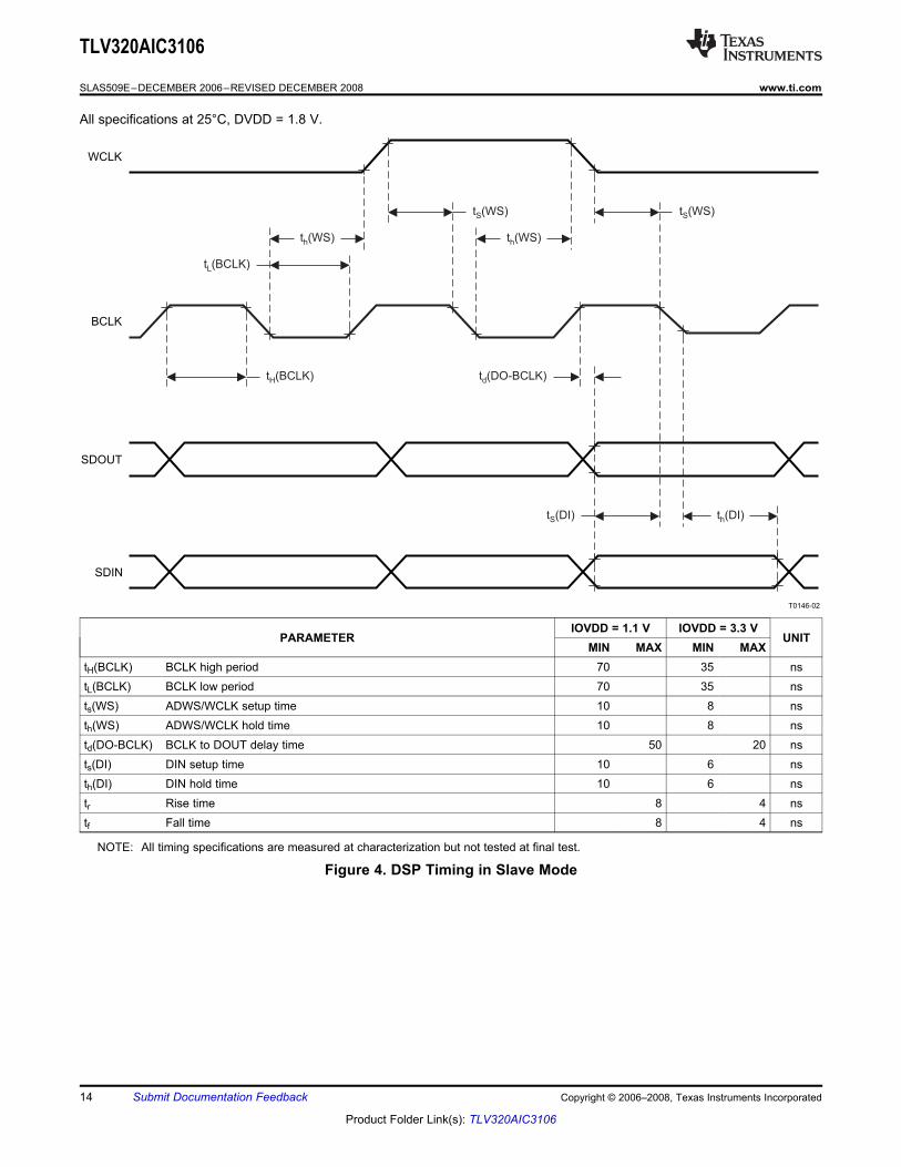
T0146-02
WCLK
BCLK
SDOUT
SDIN
t (WS)h t (WS)h
t (BCLK)L
t (DO-BCLK)d
t (DI)S
t (BCLK)H
t (DI)h
t (WS)S t (WS)S
TLV320AIC3106
SLAS509E–DECEMBER 2006–REVISED DECEMBER 2008........................................................................................................................................ www.ti.com
All specifications at 25°C, DVDD = 1.8 V.
IOVDD = 1.1 V IOVDD = 3.3 VPARAMETER UNIT
MIN MAX MIN MAXtH(BCLK) BCLK high period 70 35 nstL(BCLK) BCLK low period 70 35 nsts(WS) ADWS/WCLK setup time 10 8 nsth(WS) ADWS/WCLK hold time 10 8 nstd(DO-BCLK) BCLK to DOUT delay time 50 20 nsts(DI) DIN setup time 10 6 nsth(DI) DIN hold time 10 6 nstr Rise time 8 4 nstf Fall time 8 4 ns
NOTE: All timing specifications are measured at characterization but not tested at final test.
Figure 4. DSP Timing in Slave Mode
14 Submit Documentation Feedback Copyright © 2006–2008, Texas Instruments Incorporated
Product Folder Link(s): TLV320AIC3106
TYPICAL CHARACTERISTICS
-90
-80
-70
-60
-50
-40
-30
-20
-10
0
0 20 40 60 80 100
Headphone�Out�Power�-�mW
TH
D�-
�To
tal�
Ha
rmo
nic
�Dis
tort
ion
�-�d
B 3.6�VDD_CM�1.8_LDAC
3.3�VDD_CM�1.65_RDAC
3.6�VDD_CM�1.8_RDAC
3.3��VDD_CM1.65_LDAC
2.7��VDD_CM�1.35_LDAC
2.7�VDD_CM�1.35_RDAC
0
5
10
15
20
25
30
35
40
45
0 10 20 30 40 50 60 70
ADC,�PGA -�Setting�-�dB
SN
R�-
�Sig
na
l-To
-No
ise
�-�d
B
LINEIR�Routed�to�RADC�in�Differential�Mode,48�KSPS,�Normal�Supply�and�Temperature,Input�Signal�at�-65�dB
1.5
2
2.5
3
3.5
4
-60 -40 -20 0 20 40 60 80 100
T -�Free- Air�Temperature�-�°CA
MIC
BIA
S�V
OLTA
GE
�-�V
PGM�=�VDD
PGM�=�2�V
PGM�=�2.5�V
AV =�3.3�V,
No�LoadDD
1.5
2
2.5
3
3.5
4
2.7 2.9 3.1 3.3 3.5
V -�Supply�Voltage�-�VDD
MIC
BIA
S-�
VV
OL
TA
GE
No�Load
PGM�=�VDD
PGM�=�2�V
PGM�=�2.5�V
TLV320AIC3106
www.ti.com ........................................................................................................................................ SLAS509E–DECEMBER 2006–REVISED DECEMBER 2008
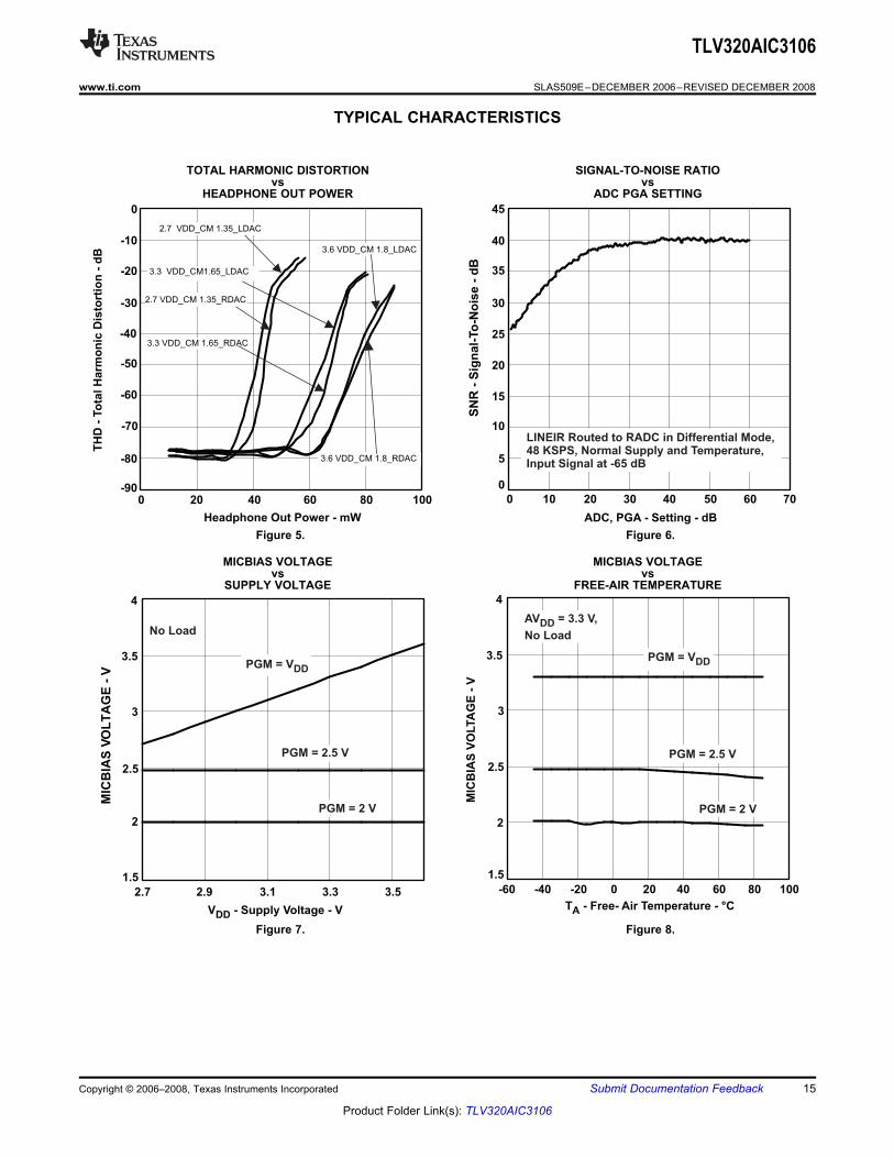
TOTAL HARMONIC DISTORTION SIGNAL-TO-NOISE RATIOvs vs
HEADPHONE OUT POWER ADC PGA SETTING
Figure 5. Figure 6.
MICBIAS VOLTAGE MICBIAS VOLTAGEvs vs
SUPPLY VOLTAGE FREE-AIR TEMPERATURE
Figure 7. Figure 8.
Copyright © 2006–2008, Texas Instruments Incorporated Submit Documentation Feedback 15
Product Folder Link(s): TLV320AIC3106
-160
-140
-120
-100
-80
-60
-40
-20
0
0 1 2 3 4 5 6 7 8 9 10 11 12 13 14 15 16 17 18 19 20
f�-�Frequency�-�kHz
Am
pli
tud
e�-
�dB
Load�=�10�k ,FS�=�48�kHz,�f =�64�kHz,
4096�Samples,AV =�DRV =�3.3�V,
!
s
DD DD
-160
-140
-120
-100
-80
-60
-40
-20
0
0 1 2 3 4 5 6 7 8 9 10 11 12 13 14 15 16 17 18 19 20
f�-�Frequency�-�kHz
Am
plitu
de�-
�dB
Load�=�10�k ,FS�=�48�kHz,�f =�64�kHz,
AV =�DRV =�3.3�V,
!
s
DD DD
-160
-140
-120
-100
-80
-60
-40
-20
0
0 1 2 3 4 5 6 7 8 9 10 11 12 13 14 15 16 17 18 19 20
f�-�Frequency�-�kHz
Am
plitu
de�-
�dB
Load�=�10�k ,FS�=�48�kHz,�f =�64�kHz,
2048�Samples,AV =�DRV =�3.3�V,
!
s
DD DD
TLV320AIC3106
SLAS509E–DECEMBER 2006–REVISED DECEMBER 2008........................................................................................................................................ www.ti.com
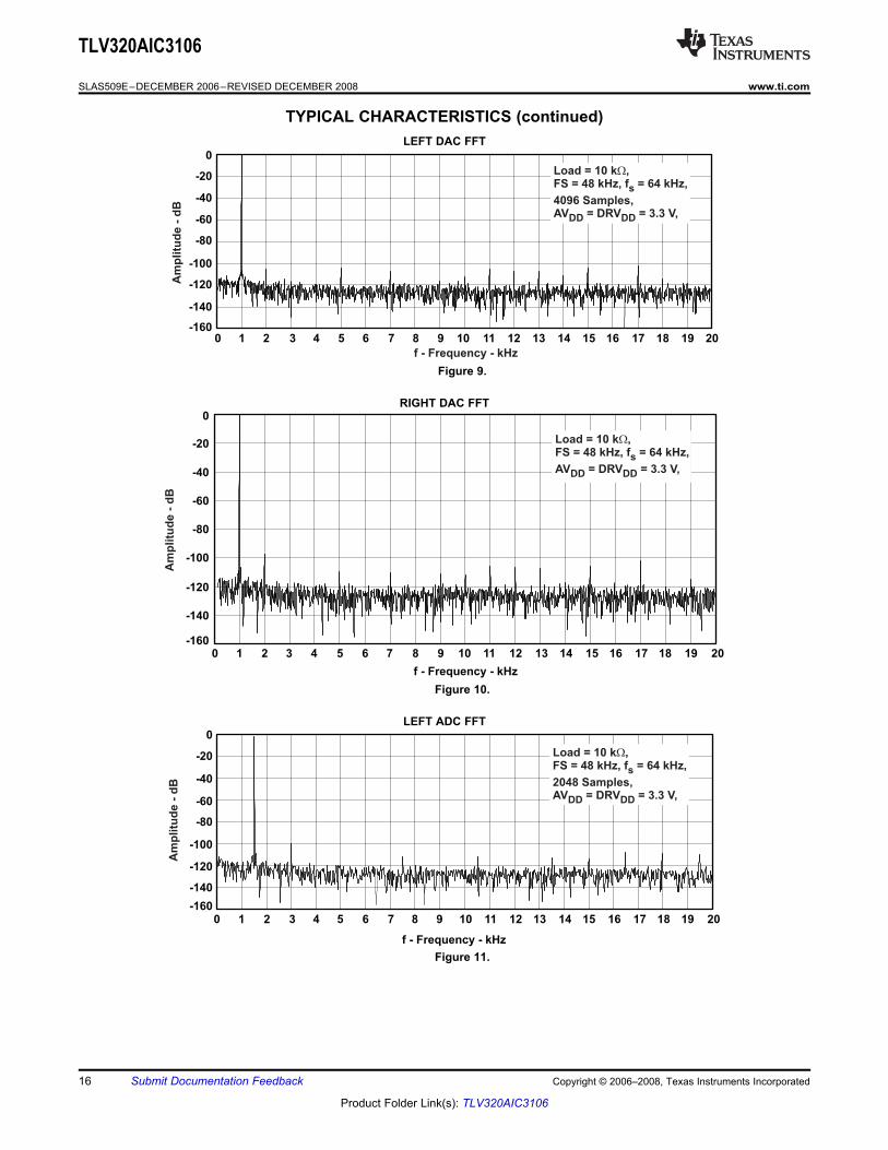
TYPICAL CHARACTERISTICS (continued)LEFT DAC FFT
Figure 9.
RIGHT DAC FFT
Figure 10.
LEFT ADC FFT
Figure 11.
16 Submit Documentation Feedback Copyright © 2006–2008, Texas Instruments Incorporated
Product Folder Link(s): TLV320AIC3106
-160
-140
-120
-100
-80
-60
-40
-20
0
0 1 2 3 4 5 6 7 8 9 10 11 12 13 14 15 16 17 18 19 20
f�-�Frequency�-�kHz
Am
plitu
de�-
�dB
Load�=�10�k ,FS�=�48�kHz,�f =�64�kHz,
2048�Samples,AV =�DRV =�3.3�V,
!
s
DD DD
TLV320AIC3106
www.ti.com ........................................................................................................................................ SLAS509E–DECEMBER 2006–REVISED DECEMBER 2008
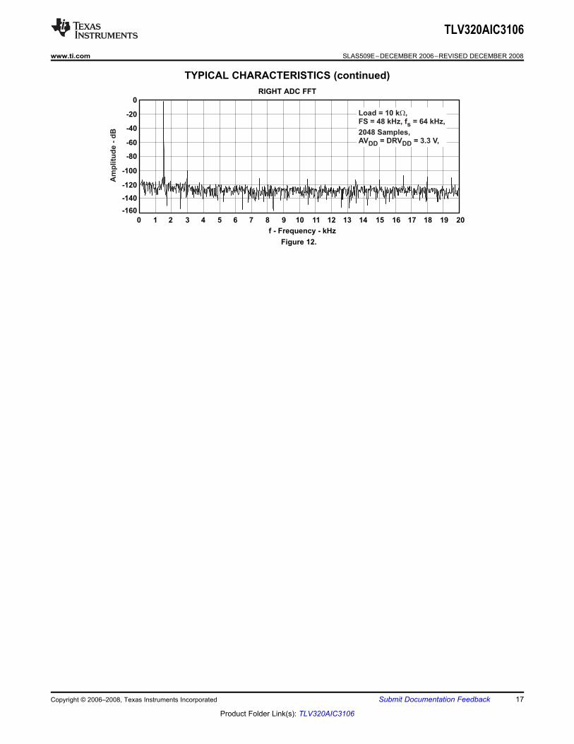
TYPICAL CHARACTERISTICS (continued)RIGHT ADC FFT
Figure 12.
Copyright © 2006–2008, Texas Instruments Incorporated Submit Documentation Feedback 17
Product Folder Link(s): TLV320AIC3106
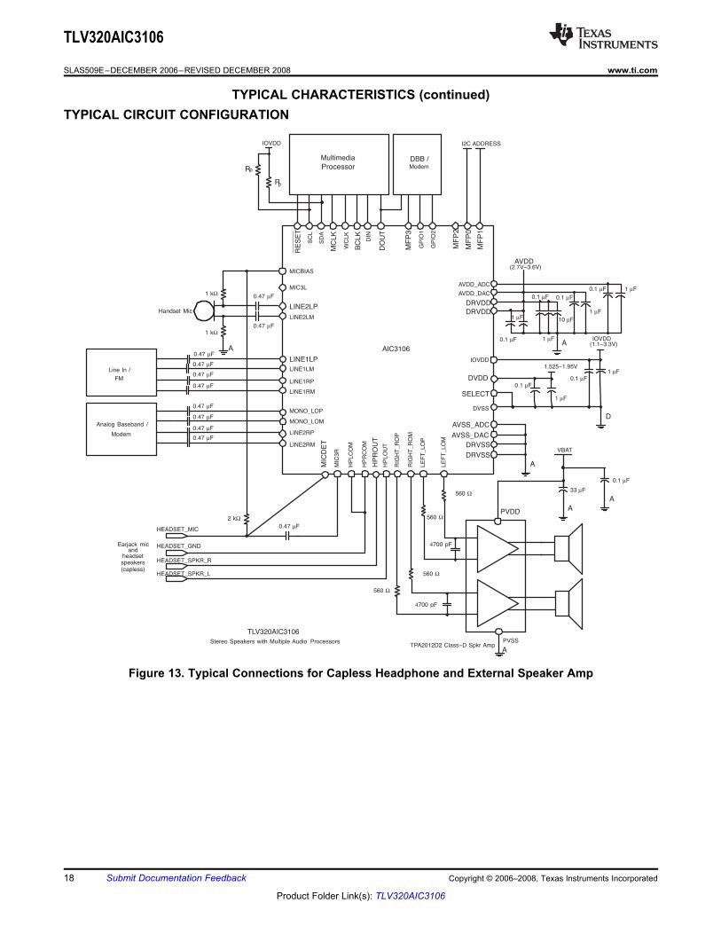
TYPICAL CIRCUIT CONFIGURATION
AIC3106
LINE2LPLINE2LM
LINE1LPLINE1LM
LINE1RPLINE1RM
MIC3L
MICBIAS
A
AVDD_DAC
AVSS_DAC
DRVDD
DRVSS
PVDD
DVSS
IOVDD
DRVDD
DRVSS
AVDD_ADC
AVSS_ADC
A
D
1.525−1.95V
IOVDD(1.1−3.3V)
LEFT
_LO
P
LEFT
_LO
M
RIG
HT_
RO
P
RIG
HT_
RO
M
HPR
OU
T
HPL
CO
M
HPR
CO
M
MIC
DET
A
AVDD(2.7V−3.6V)
TLV320AIC3106Stereo Speakers with Multiple Audio Processors
MIC
3R
HPL
OU
T
HEADSET_MIC
HEADSET_GND
HEADSET_SPKR_R
HEADSET_SPKR_L
A
A
VBAT
PVSS
DVDD
Earjack micand
headsetspeakers(capless)
Handset Mic
Analog Baseband /Modem
MONO_LOPMONO_LOM
LINE2RP
LINE2RM
Line In /FM
MultimediaProcessor
DO
UT
MFP
0
BCLK DIN
MC
LK
GPI
O1
GPI
O2
SCL
SDA
WC
LK
MFP
2
MFP
1
RES
ET
MFP
3
SELECT
DBB /ModemRp
Rp
IOVDD I2C ADDRESS
TPA2012D2 Class−D Spkr Amp
1 kΩ
1 kΩ
0.47 µF
0.47 µF
0.47 µF
0.47 µF2 kΩ
560 Ω
560 Ω
560 Ω
4700 pF
4700 pF
560 Ω
1 µF0.1 µF
0.47 µF
0.47 µF0.47 µF
0.47 µF
0.47 µF
0.47 µF0.47 µF
1 µF
0.1 µF
0.1 µF
1 µF
0.1 µF
10 µF
1 µF
1 µF0.1 µF
1 µF
0.1 µF
33 µFA
0.1 µF
TLV320AIC3106
SLAS509E–DECEMBER 2006–REVISED DECEMBER 2008........................................................................................................................................ www.ti.com
TYPICAL CHARACTERISTICS (continued)
Figure 13. Typical Connections for Capless Headphone and External Speaker Amp
18 Submit Documentation Feedback Copyright © 2006–2008, Texas Instruments Incorporated
Product Folder Link(s): TLV320AIC3106
OVERVIEW
HARDWARE RESET
DIGITAL CONTROL SERIAL INTERFACE
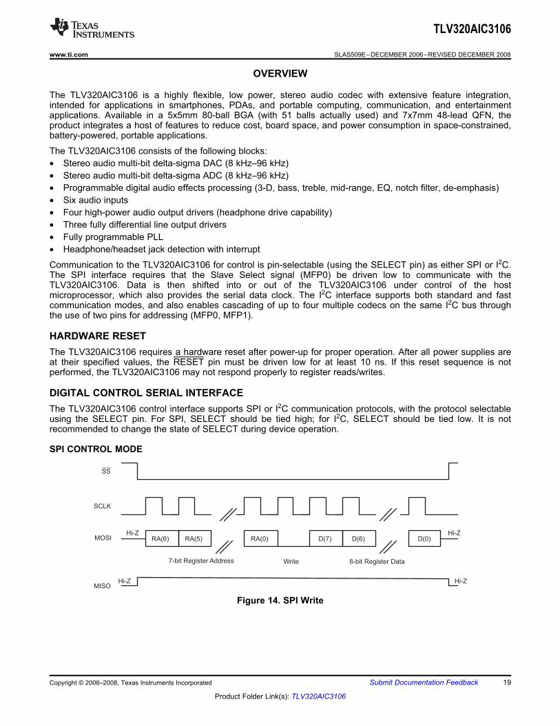
SPI CONTROL MODE
RA(6) RA(5) RA(0) D(7) D(6) D(0)
7-bit�Register Address Write 8-bit�Register�Data
SS
SCLK
MOSI
MISO
Hi-Z Hi-Z
Hi-Z Hi-Z
TLV320AIC3106
www.ti.com ........................................................................................................................................ SLAS509E–DECEMBER 2006–REVISED DECEMBER 2008
The TLV320AIC3106 is a highly flexible, low power, stereo audio codec with extensive feature integration,intended for applications in smartphones, PDAs, and portable computing, communication, and entertainmentapplications. Available in a 5x5mm 80-ball BGA (with 51 balls actually used) and 7x7mm 48-lead QFN, theproduct integrates a host of features to reduce cost, board space, and power consumption in space-constrained,battery-powered, portable applications.
The TLV320AIC3106 consists of the following blocks:• Stereo audio multi-bit delta-sigma DAC (8 kHz–96 kHz)• Stereo audio multi-bit delta-sigma ADC (8 kHz–96 kHz)• Programmable digital audio effects processing (3-D, bass, treble, mid-range, EQ, notch filter, de-emphasis)• Six audio inputs• Four high-power audio output drivers (headphone drive capability)• Three fully differential line output drivers• Fully programmable PLL• Headphone/headset jack detection with interrupt
Communication to the TLV320AIC3106 for control is pin-selectable (using the SELECT pin) as either SPI or I2C.The SPI interface requires that the Slave Select signal (MFP0) be driven low to communicate with theTLV320AIC3106. Data is then shifted into or out of the TLV320AIC3106 under control of the hostmicroprocessor, which also provides the serial data clock. The I2C interface supports both standard and fastcommunication modes, and also enables cascading of up to four multiple codecs on the same I2C bus throughthe use of two pins for addressing (MFP0, MFP1).
The TLV320AIC3106 requires a hardware reset after power-up for proper operation. After all power supplies areat their specified values, the RESET pin must be driven low for at least 10 ns. If this reset sequence is notperformed, the TLV320AIC3106 may not respond properly to register reads/writes.
The TLV320AIC3106 control interface supports SPI or I2C communication protocols, with the protocol selectableusing the SELECT pin. For SPI, SELECT should be tied high; for I2C, SELECT should be tied low. It is notrecommended to change the state of SELECT during device operation.
Figure 14. SPI Write
Copyright © 2006–2008, Texas Instruments Incorporated Submit Documentation Feedback 19
Product Folder Link(s): TLV320AIC3106

RA(6) RA(5) RA(0) Don’t�Care
7-bit�Register Address Read 8-bit�Register�Data
SS
SCLK
MOSI
MISO
Hi-Z Hi-Z
D(7) D(6) D(0)Hi-Z Hi-Z
SPI COMMUNICATION PROTOCOL
TLV320AIC3106
SLAS509E–DECEMBER 2006–REVISED DECEMBER 2008........................................................................................................................................ www.ti.com
Figure 15. SPI Read
In the SPI control mode, the TLV320AIC3106 uses the pins MFP0=SSB, MFP1=SCLK, MFP2=MISO,MFP3=MOSI as a standard SPI port with clock polarity setting of 0 (typical microprocessor SPI control bit CPOL= 0). The SPI port allows full-duplex, synchronous, serial communication between a host processor (the master)and peripheral devices (slaves). The SPI master (in this case, the host processor) generates the synchronizingclock (driven onto SCLK) and initiates transmissions. The SPI slave devices (such as the TLV320AIC3106)depend on a master to start and synchronize transmissions.
A transmission begins when initiated by an SPI master. The byte from the SPI master begins shifting in on theslave MOSI pin under the control of the master serial clock (driven onto SCLK). As the byte shifts in on the MOSIpin, a byte shifts out on the MISO pin to the master shift register.
The TLV320AIC3106 interface is designed so that with a clock phase bit setting of 1 (typical microprocessor SPIcontrol bit CPHA = 1), the master begins driving its MOSI pin and the slave begins driving its MISO pin on thefirst serial clock edge. The SSB pin can remain low between transmissions; however, the TLV320AIC3106 onlyinterprets the first 8 bits transmitted after the falling edge of SSB as a command byte, and the next 8 bits as adata byte only if writing to a register. Reserved register bits should be written to their default values.
The TLV320AIC3106 is entirely controlled by registers. Reading and writing these registers is accomplished bythe use of an 8-bit command, which is sent to the MOSI pin of the part prior to the data for that register. Thecommand is constructed as shown in Table X. The first 7 bits specify the register address which is being writtenor read, from 0 to 127 (decimal). The command word ends with an R/W bit, which specifies the direction of dataflow on the serial bus. In the case of a register write, the R/W bit should be set to 0. A second byte of data issent to the MOSI pin and contains the data to be written to the register.
Reading of registers is accomplished in similar fashion. The 8-bit command word sends the 7-bit registeraddress, followed by R/W bit = 1 to signify a register read is occurring,. The 8-bit register data is then clocked outof the part on the MISO pin during the second 8 SCLK clocks in the frame.
Command WordBit 7 Bit 6 Bit 5 Bit 4 Bit 3 Bit 2 Bit 1 Bit 0ADDR6 ADDR5 ADDR4 ADDR3 ADDR2 ADDR1 ADDR0 R/W
The register map of the TLV320AIC3106 actually consists of multiple pages of registers, with each pagecontaining 128 registers. The register at address zero on each page is used as a page-control register, andwriting to this register determines the active page for the device. All subsequent read/write operations will accessthe page that is active at the time, unless a register write is performed to change the active page. Only twopages of registers are implemented in this product, with the active page defaulting to page 0 upon device reset.
For example, at device reset, the active page defaults to page 0, and thus all register read/write operations foraddresses 1 to 127 will access registers in page 0. If registers on page 1 must be accessed, the user must writethe 8-bit sequence 0x01 to register 0, the page control register, to change the active page from page 0 to page 1.
20 Submit Documentation Feedback Copyright © 2006–2008, Texas Instruments Incorporated
Product Folder Link(s): TLV320AIC3106
CONTINUOUS READ / WRITE OPERATION
I2C CONTROL MODE
TLV320AIC3106
www.ti.com ........................................................................................................................................ SLAS509E–DECEMBER 2006–REVISED DECEMBER 2008
After this write, it is recommended the user also read back the page control register, to safely ensure the changein page control has occurred properly. Future read/write operations to addresses 1 to 127 will now accessregisters in page 1. When page 0 registers must be accessed again, the user writes the 8-bit sequence 0x00 toregister 0, the page control register, to change the active page back to page 0. After a recommended read of thepage control register, all further read/write operations to addresses 1 to 127 will now access page 0 registersagain.
Limitation on Register WritingWhen writing registers in SPI mode related to the audio output drivers mux, mix, gain configuration, etc., do notuse the auto-increment mode. In addition, between two successive writes to these registers, the host shouldkeep MFP0 (SPI chip select) high for at least 6.25us, to ensure that the register writes have occurred properly.
The TLV320AIC3106 includes the ability to read/write registers continuously, without needing to provide anaddress for every register accessed. In SPI mode, a continuous write is executed by transitioning MFP0 (SPIchip select) low to start the frame, sending the first 8-bit command word to read/write a particular register, andthen sending multiple bytes of register data, intended for the addressed register and those following. Acontinuous read is done similarly, with multiple bytes read in from the addressed register and the followingregisters on the page. When the MFP0 (SPI chip select) pin is transitioned high again, the frame ends, as doesthe continuous read/write operation. A new frame must begin again with a new command word, to start the nextbus transaction.
Note that this continuous read/write operation does not continue past a page boundary. The user should notattempt to read/write past the end of a page, since this may result in undesirable operation.
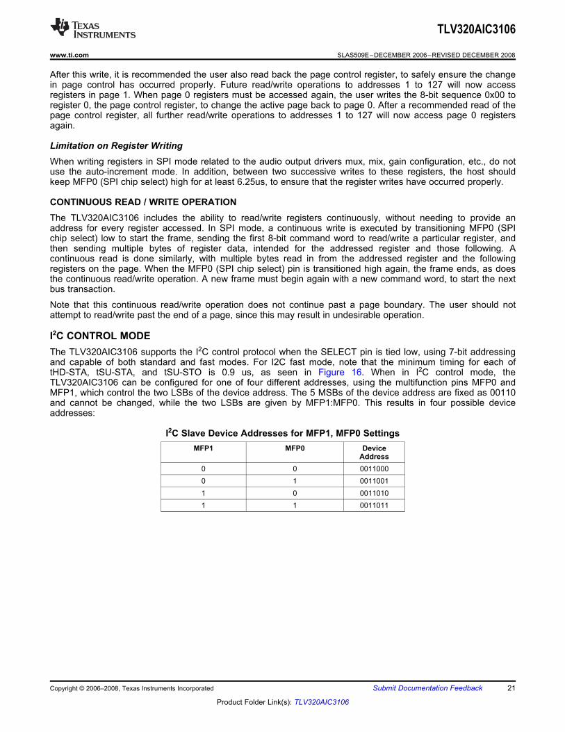
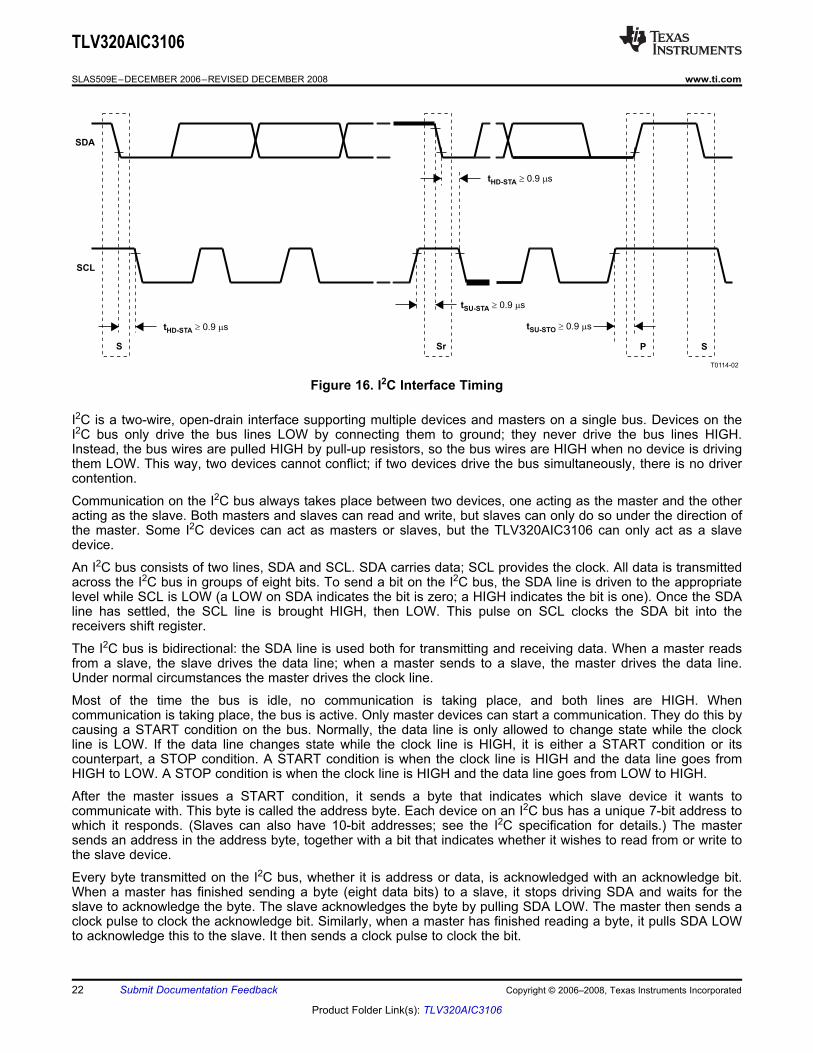
The TLV320AIC3106 supports the I2C control protocol when the SELECT pin is tied low, using 7-bit addressingand capable of both standard and fast modes. For I2C fast mode, note that the minimum timing for each oftHD-STA, tSU-STA, and tSU-STO is 0.9 us, as seen in Figure 16. When in I2C control mode, theTLV320AIC3106 can be configured for one of four different addresses, using the multifunction pins MFP0 andMFP1, which control the two LSBs of the device address. The 5 MSBs of the device address are fixed as 00110and cannot be changed, while the two LSBs are given by MFP1:MFP0. This results in four possible deviceaddresses:
I2C Slave Device Addresses for MFP1, MFP0 SettingsMFP1 MFP0 Device
Address0 0 00110000 1 00110011 0 00110101 1 0011011
Copyright © 2006–2008, Texas Instruments Incorporated Submit Documentation Feedback 21
Product Folder Link(s): TLV320AIC3106
SDA
SCL
tHD-STA 0.9 s! "
tSU-STO 0.9 s! "
P S
tSU-STA 0.9 s! "
Sr
tHD-STA 0.9 s! "
S
T0114-02
TLV320AIC3106
SLAS509E–DECEMBER 2006–REVISED DECEMBER 2008........................................................................................................................................ www.ti.com
Figure 16. I2C Interface Timing
I2C is a two-wire, open-drain interface supporting multiple devices and masters on a single bus. Devices on theI2C bus only drive the bus lines LOW by connecting them to ground; they never drive the bus lines HIGH.Instead, the bus wires are pulled HIGH by pull-up resistors, so the bus wires are HIGH when no device is drivingthem LOW. This way, two devices cannot conflict; if two devices drive the bus simultaneously, there is no drivercontention.
Communication on the I2C bus always takes place between two devices, one acting as the master and the otheracting as the slave. Both masters and slaves can read and write, but slaves can only do so under the direction ofthe master. Some I2C devices can act as masters or slaves, but the TLV320AIC3106 can only act as a slavedevice.
An I2C bus consists of two lines, SDA and SCL. SDA carries data; SCL provides the clock. All data is transmittedacross the I2C bus in groups of eight bits. To send a bit on the I2C bus, the SDA line is driven to the appropriatelevel while SCL is LOW (a LOW on SDA indicates the bit is zero; a HIGH indicates the bit is one). Once the SDAline has settled, the SCL line is brought HIGH, then LOW. This pulse on SCL clocks the SDA bit into thereceivers shift register.
The I2C bus is bidirectional: the SDA line is used both for transmitting and receiving data. When a master readsfrom a slave, the slave drives the data line; when a master sends to a slave, the master drives the data line.Under normal circumstances the master drives the clock line.
Most of the time the bus is idle, no communication is taking place, and both lines are HIGH. Whencommunication is taking place, the bus is active. Only master devices can start a communication. They do this bycausing a START condition on the bus. Normally, the data line is only allowed to change state while the clockline is LOW. If the data line changes state while the clock line is HIGH, it is either a START condition or itscounterpart, a STOP condition. A START condition is when the clock line is HIGH and the data line goes fromHIGH to LOW. A STOP condition is when the clock line is HIGH and the data line goes from LOW to HIGH.
After the master issues a START condition, it sends a byte that indicates which slave device it wants tocommunicate with. This byte is called the address byte. Each device on an I2C bus has a unique 7-bit address towhich it responds. (Slaves can also have 10-bit addresses; see the I2C specification for details.) The mastersends an address in the address byte, together with a bit that indicates whether it wishes to read from or write tothe slave device.
Every byte transmitted on the I2C bus, whether it is address or data, is acknowledged with an acknowledge bit.When a master has finished sending a byte (eight data bits) to a slave, it stops driving SDA and waits for theslave to acknowledge the byte. The slave acknowledges the byte by pulling SDA LOW. The master then sends aclock pulse to clock the acknowledge bit. Similarly, when a master has finished reading a byte, it pulls SDA LOWto acknowledge this to the slave. It then sends a clock pulse to clock the bit.
22 Submit Documentation Feedback Copyright © 2006–2008, Texas Instruments Incorporated
Product Folder Link(s): TLV320AIC3106
DA(6) DA(0) RA(7) RA(0) D(7) D(0)
Start(M)
7-bit Device Address(M)
Write(M)
SlaveAck(S)
8-bit Register Address(M)
SlaveAck(S)
8-bit Register Data(M)
Stop(M)
SlaveAck(S)
SDA
SCL
(M) => SDA Controlled by Master(S) => SDA Controlled by Slave
DA(6) DA(0) RA(7) RA(0)
Start(M)
7-bit Device Address(M)
Write(M)
SlaveAck(S)
8-bit Register Address(M)
SlaveAck(S)
SDA
SCL
DA(6) DA(0)
7-bit Device Address(M)
Read(M)
SlaveAck(S)
D(7) D(0)
8-bit Register Data(S)
Stop(M)
MasterNo Ack
(M)
RepeatStart(M)
(M) => SDA Controlled by Master(S) => SDA Controlled by Slave
I2C BUS DEBUG IN A GLITCHED SYSTEM
DIGITAL AUDIO DATA SERIAL INTERFACE
TLV320AIC3106
www.ti.com ........................................................................................................................................ SLAS509E–DECEMBER 2006–REVISED DECEMBER 2008
A not-acknowledge is performed by simply leaving SDA HIGH during an acknowledge cycle. If a device is notpresent on the bus, and the master attempts to address it, it will receive a notíacknowledge because no deviceis present at that address to pull the line LOW.
When a master has finished communicating with a slave, it may issue a STOP condition. When a STOPcondition is issued, the bus becomes idle again. A master may also issue another START condition. When aSTART condition is issued while the bus is active, it is called a repeated START condition.
The TLV320AIC3106 also responds to and acknowledges a General Call, which consists of the master issuing acommand with a slave address byte of 00H.
Figure 17. I2C Write
Figure 18. I2C Read
In the case of an I2C register write, if the master does not issue a STOP condition, then the device entersauto-increment mode. So in the next eight clocks, the data on SDA is treated as data for the next incrementalregister.
Similarly, in the case of an I2C register read, after the device has sent out the 8-bit data from the addressedregister, if the master issues an ACKNOWLEDGE, the slave takes over control of SDA bus and transmit for thenext 8 clocks the data of the next incremental register.
Occasionally, some systems may encounter noise or glitches on the I2C bus. In the unlikely event that thisaffects bus performance, then it can be useful to use the I2C Debug register. This feature terminates the I2C buserror allowing this I2C device and system to resume communications. The I2C bus error detector is enabled bydefault. The TLV320AIC3106 I2C error detector status can be read from Page 0, Register 107, bit D0. If desired,the detector can be disabled by writing to Page 0, Register 107, bit D2.
Audio data is transferred between the host processor and the TLV320AIC3106 via the digital audio data serialinterface, or audio bus. The audio bus on this device is very flexible, including left or right justified data options,support for I2S or PCM protocols, programmable data length options, a TDM mode for multichannel operation,very flexible master/slave configurability for each bus clock line, and the ability to communicate with multipledevices within a system directly.
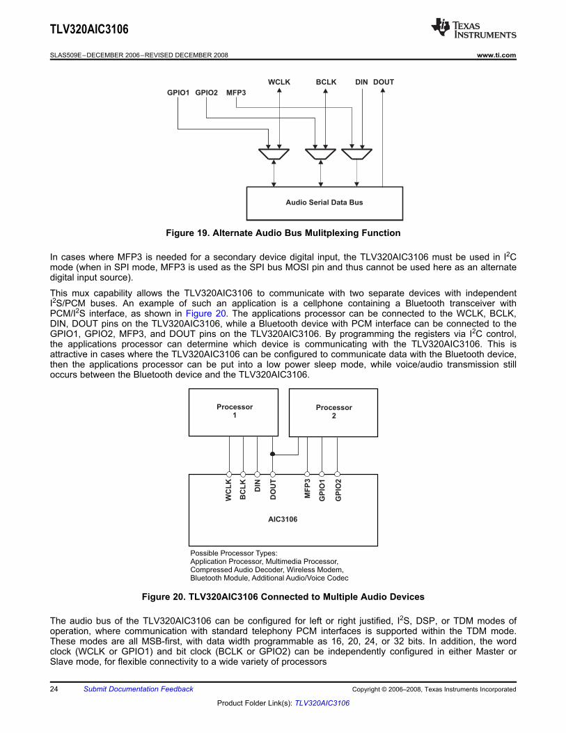
The data serial interface uses two sets of pins for communication between external devices, with the particularpin used controlled through register programming. This configuration is shown in Figure 19 below.
Copyright © 2006–2008, Texas Instruments Incorporated Submit Documentation Feedback 23
Product Folder Link(s): TLV320AIC3106
Audio�Serial�Data�Bus
DOUT
GPIO1 GPIO2 MFP3
WCLK BCLK DIN
Possible�Processor Types:Application�Processor,�Multimedia�Processor,Compressed Audio�Decoder,�Wireless�Modem,Bluetooth�Module, Additional Audio/Voice�Codec
Processor
2
Processor
1
GP
IO2
WC
LK
BC
LK
DIN
DO
UT
MF
P3
GP
IO1
AIC3106
TLV320AIC3106
SLAS509E–DECEMBER 2006–REVISED DECEMBER 2008........................................................................................................................................ www.ti.com
Figure 19. Alternate Audio Bus Mulitplexing Function
In cases where MFP3 is needed for a secondary device digital input, the TLV320AIC3106 must be used in I2Cmode (when in SPI mode, MFP3 is used as the SPI bus MOSI pin and thus cannot be used here as an alternatedigital input source).
This mux capability allows the TLV320AIC3106 to communicate with two separate devices with independentI2S/PCM buses. An example of such an application is a cellphone containing a Bluetooth transceiver withPCM/I2S interface, as shown in Figure 20. The applications processor can be connected to the WCLK, BCLK,DIN, DOUT pins on the TLV320AIC3106, while a Bluetooth device with PCM interface can be connected to theGPIO1, GPIO2, MFP3, and DOUT pins on the TLV320AIC3106. By programming the registers via I2C control,the applications processor can determine which device is communicating with the TLV320AIC3106. This isattractive in cases where the TLV320AIC3106 can be configured to communicate data with the Bluetooth device,then the applications processor can be put into a low power sleep mode, while voice/audio transmission stilloccurs between the Bluetooth device and the TLV320AIC3106.
Figure 20. TLV320AIC3106 Connected to Multiple Audio Devices
The audio bus of the TLV320AIC3106 can be configured for left or right justified, I2S, DSP, or TDM modes ofoperation, where communication with standard telephony PCM interfaces is supported within the TDM mode.These modes are all MSB-first, with data width programmable as 16, 20, 24, or 32 bits. In addition, the wordclock (WCLK or GPIO1) and bit clock (BCLK or GPIO2) can be independently configured in either Master orSlave mode, for flexible connectivity to a wide variety of processors
24 Submit Documentation Feedback Copyright © 2006–2008, Texas Instruments Incorporated
Product Folder Link(s): TLV320AIC3106

RIGHT-JUSTIFIED MODE
BCLK
WCLK
SDIN/SDOUT
1 00 1 0
1/fs
LSBMSB
Left�Channel Right�Channel
2 2n!1 n!3n!2 n!1 n!3n!2
LEFT-JUSTIFIED MODE
TLV320AIC3106
www.ti.com ........................................................................................................................................ SLAS509E–DECEMBER 2006–REVISED DECEMBER 2008
The word clock (WCLK or GPIO1) is used to define the beginning of a frame, and may be programmed as eithera pulse or a square-wave signal. The frequency of this clock corresponds to the maximum of the selected ADCand DAC sampling frequencies.
The bit clock (BCLK or GPIO2) is used to clock in and out the digital audio data across the serial bus. When inMaster mode, this signal can be programmed in two further modes: continuous transfer mode, and 256-clockmode. In continuous transfer mode, only the minimal number of bit clocks needed to transfer the audio data aregenerated, so in general the number of bit clocks per frame will be two times the data width. For example, if datawidth is chosen as 16 bits, then 32 bit clocks will be generated per frame. If the bit clock signal in master modewill be used by a PLL in another device, it is recommended that the 16-bit or 32-bit data width selections beused. These cases result in a low jitter bit clock signal being generated, having frequencies of 32 × fS or 64 × fS.In the cases of 20-bit and 24-bt data width in master mode, the bit clocks generated in each frame will not all beof equal period, due to the device not having a clean 40 × fS or 48 × fS clock signal readily available. Theaverage frequency of the bit clock signal is still accurate in these cases (being 40 × fS or 48 × fS), but theresulting clock signal has higher jitter than in the 16-bit and 32-bit cases.
In 256-clock mode, a constant 256 bit clocks per frame are generated, independent of the data width chosen.The TLV320AIC3106 further includes programmability to 3-state the DOUT line during all bit clocks when validdata is not being sent. By combining this capability with the ability to program at what bit clock in a frame theaudio data will begin, time-division multiplexing (TDM) can be accomplished, resulting in multiple codecs able touse a single audio serial data bus.
When the audio serial data bus is powered down while configured in master mode, the pins associated with theinterface will be put into a 3-state output condition.
In right-justified mode, the LSB of the left channel is valid on the rising edge of the bit clock preceding the fallingedge of word clock. Similarly, the LSB of the right channel is valid on the rising edge of the bit clock precedingthe rising edge of the word clock.
Figure 21. Right-Justified Serial Bus Mode Operation
In left-justified mode, the MSB of the right channel is valid on the rising edge of the bit clock following the fallingedge of the word clock. Similarly the MSB of the left channel is valid on the rising edge of the bit clock followingthe rising edge of the word clock.
Copyright © 2006–2008, Texas Instruments Incorporated Submit Documentation Feedback 25
Product Folder Link(s): TLV320AIC3106

n-1 n-2 n-3 n-1 n-2 n-3
I2S MODE
n-1 n-2 n-3 n-1 n-2 n-3
DSP MODE
TLV320AIC3106
SLAS509E–DECEMBER 2006–REVISED DECEMBER 2008........................................................................................................................................ www.ti.com
Figure 22. Left-Justified Serial Data Bus Mode Operation
In I2S mode, the MSB of the left channel is valid on the second rising edge of the bit clock after the falling edgeof the word clock. Similarly the MSB of the right channel is valid on the second rising edge of the bit clock afterthe rising edge of the word clock.
Figure 23. I2S Serial Data Bus Mode Operation
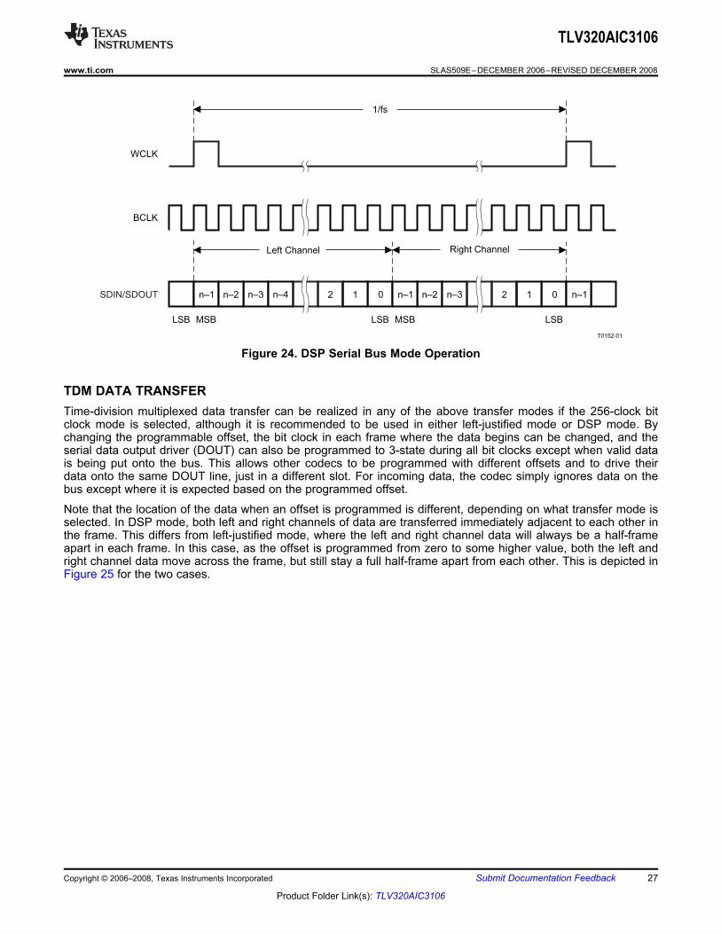
In DSP mode, the rising edge of the word clock starts the data transfer with the left channel data first andimmediately followed by the right channel data. Each data bit is valid on the falling edge of the bit clock.
26 Submit Documentation Feedback Copyright © 2006–2008, Texas Instruments Incorporated
Product Folder Link(s): TLV320AIC3106
BCLK
WCLK
0 0
T0152-01
1/fs
LSB LSBLSB MSB MSB
Left�Channel Right�Channel
1 12 2SDIN/SDOUT n–1 n–1n–1n–2 n–3 n–3n–4 n–2
TDM DATA TRANSFER
TLV320AIC3106
www.ti.com ........................................................................................................................................ SLAS509E–DECEMBER 2006–REVISED DECEMBER 2008
Figure 24. DSP Serial Bus Mode Operation
Time-division multiplexed data transfer can be realized in any of the above transfer modes if the 256-clock bitclock mode is selected, although it is recommended to be used in either left-justified mode or DSP mode. Bychanging the programmable offset, the bit clock in each frame where the data begins can be changed, and theserial data output driver (DOUT) can also be programmed to 3-state during all bit clocks except when valid datais being put onto the bus. This allows other codecs to be programmed with different offsets and to drive theirdata onto the same DOUT line, just in a different slot. For incoming data, the codec simply ignores data on thebus except where it is expected based on the programmed offset.
Note that the location of the data when an offset is programmed is different, depending on what transfer mode isselected. In DSP mode, both left and right channels of data are transferred immediately adjacent to each other inthe frame. This differs from left-justified mode, where the left and right channel data will always be a half-frameapart in each frame. In this case, as the offset is programmed from zero to some higher value, both the left andright channel data move across the frame, but still stay a full half-frame apart from each other. This is depicted inFigure 25 for the two cases.
Copyright © 2006–2008, Texas Instruments Incorporated Submit Documentation Feedback 27
Product Folder Link(s): TLV320AIC3106

N-1 N-2 1 0 N-1 N-2 1 0
wordclock
bit clock
datain/out
Right�Channel�Data
Right�Channel�Data
Left�Channel�Data
Left�Channel�Data
N-1 N-2 1 0 N-1 N-2 1 0
wordclock
bit clock
datain/out
DSP Mode
Left�Justified�Mode
offset
offset
offset
AUDIO DATA CONVERTERS
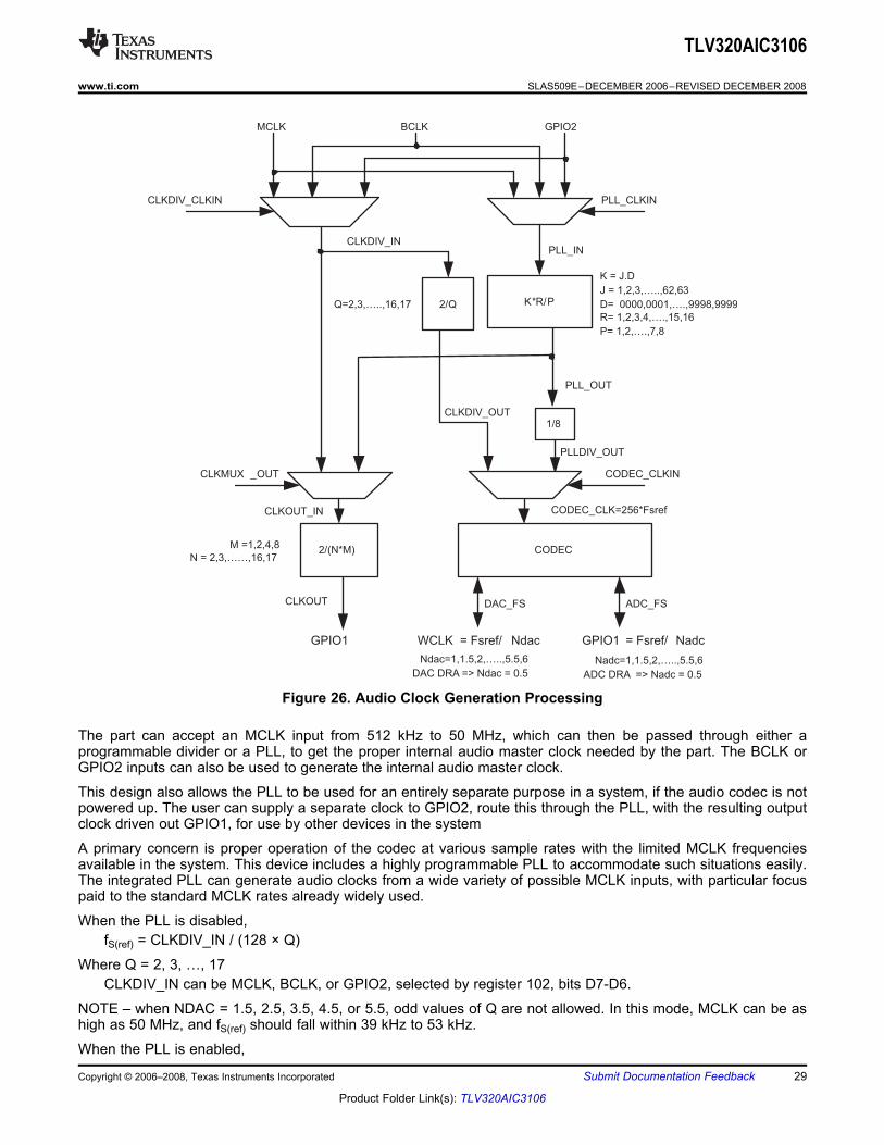
AUDIO CLOCK GENERATION
TLV320AIC3106
SLAS509E–DECEMBER 2006–REVISED DECEMBER 2008........................................................................................................................................ www.ti.com
Figure 25. DSP Mode and Left Justified Modes, Showing theEffect of a Programmed Data Word Offset
The TLV320AIC3106 supports the following standard audio sampling rates: 8 kHz, 11.025 kHz, 12 kHz, 16 kHz,22.05 kHz, 24 kHz, 32 kHz, 44.1 kHz, 48 kHz, 88.2 kHz, and 96 kHz. The converters can also operate atdifferent sampling rates in various combinations, which are described further below.
The data converters are based on the concept of an fS(ref) rate that is used internal to the part, and it is related tothe actual sampling rates of the converters through a series of ratios. For typical sampling rates, fS(ref) will beeither 44.1 kHz or 48 kHz, although it can realistically be set over a wider range of rates up to 53 kHz, withadditional restrictions applying if the PLL is used. This concept is used to set the sampling rates of the ADC andDAC, and also to enable high quality playback of low sampling rate data, without high frequency audible noisebeing generated.
The sampling rate of the ADC and DAC can be set to fS(ref)/NDAC or 2×fS(ref)/NDAC, with NDAC being 1, 1.5, 2,2.5, 3, 3.5, 4, 4.5, 5, 5.5, or 6.
While only one fS(ref) can be used at a time in the part, the ADC and DAC sampling rates can differ from eachother by using different NADC and NDAC divider ratios for each. For example, with fS(ref)=44.1-kHz, the DACsampling rate can be set to 44.1-kHz by using NDAC=1, while the ADC sampling rate can be set to 8.018-kHz byusing NADC=5.5.
When the ADCs and DACs are operating at different sampling rates, an additional word clock is required, toprovide information regarding where data begins for the ADC versus the DAC. In this case, the standard bit clocksignal (which can be supplied through the BCLK pin or through GPIO2) is used to transfer both ADC and DACdata, the standard word clock signal is used to identify the start of the DAC data, and a separate ADC word clocksignal (denoted ADWK) is used. This clock can be supplied or generated from GPIO1 at the same time the DACword clock is supplied or generated from WCLK.
The audio converters in the TLV320AIC3106 need an internal audio master clock at a frequency of 256 × fS(ref),which can be obtained in a variety of manners from an external clock signal applied to the device.
A more detailed diagram of the audio clock section of the TLV320AIC3106 is shown in Figure 26.
28 Submit Documentation Feedback Copyright © 2006–2008, Texas Instruments Incorporated
Product Folder Link(s): TLV320AIC3106
K*R/P2/Q
GPIO2
PLL_CLKIN
CODEC
CODEC_CLKIN
PLL_OUT
K�=�J.D
J�=�1,2,3,…..,62,63
D=��0000,0001,….,9998,9999R=�1,2,3,4,….,15,16
P=�1,2,….,7,8
Q=2,3,…..,16,17
MCLK BCLK
CLKDIV_INPLL_IN
WCLK =�Fsref/ Ndac GPIO1 =�Fsref/ Nadc
ADC_FSDAC_FS
Ndac=1,1.5,2,…..,5.5,6
DAC�DRA =>�Ndac�=�0.5Nadc=1,1.5,2,…..,5.5,6
ADC�DRA =>�Nadc�=�0.5
CODEC_CLK=256*Fsref
CLKDIV_OUT1/8
PLLDIV_OUT
CLKDIV_CLKIN
2/(N*M)
CLKMUX _OUT
GPIO1
M�=1,2,4,8N�=�2,3,……,16,17
CLKOUT
CLKOUT_IN
TLV320AIC3106
www.ti.com ........................................................................................................................................ SLAS509E–DECEMBER 2006–REVISED DECEMBER 2008
Figure 26. Audio Clock Generation Processing
The part can accept an MCLK input from 512 kHz to 50 MHz, which can then be passed through either aprogrammable divider or a PLL, to get the proper internal audio master clock needed by the part. The BCLK orGPIO2 inputs can also be used to generate the internal audio master clock.
This design also allows the PLL to be used for an entirely separate purpose in a system, if the audio codec is notpowered up. The user can supply a separate clock to GPIO2, route this through the PLL, with the resulting outputclock driven out GPIO1, for use by other devices in the system
A primary concern is proper operation of the codec at various sample rates with the limited MCLK frequenciesavailable in the system. This device includes a highly programmable PLL to accommodate such situations easily.The integrated PLL can generate audio clocks from a wide variety of possible MCLK inputs, with particular focuspaid to the standard MCLK rates already widely used.
When the PLL is disabled,fS(ref) = CLKDIV_IN / (128 × Q)
Where Q = 2, 3, …, 17CLKDIV_IN can be MCLK, BCLK, or GPIO2, selected by register 102, bits D7-D6.
NOTE – when NDAC = 1.5, 2.5, 3.5, 4.5, or 5.5, odd values of Q are not allowed. In this mode, MCLK can be ashigh as 50 MHz, and fS(ref) should fall within 39 kHz to 53 kHz.
When the PLL is enabled,
Copyright © 2006–2008, Texas Instruments Incorporated Submit Documentation Feedback 29
Product Folder Link(s): TLV320AIC3106
TLV320AIC3106
SLAS509E–DECEMBER 2006–REVISED DECEMBER 2008........................................................................................................................................ www.ti.com
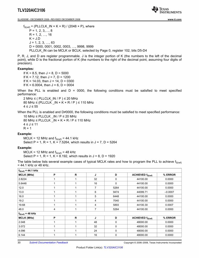
fS(ref) = (PLLCLK_IN × K × R) / (2048 × P), whereP = 1, 2, 3,…, 8R = 1, 2, …, 16K = J.DJ = 1, 2, 3, …, 63D = 0000, 0001, 0002, 0003, …, 9998, 9999PLLCLK_IN can be MCLK or BCLK, selected by Page 0, register 102, bits D5-D4
P, R, J, and D are register programmable. J is the integer portion of K (the numbers to the left of the decimalpoint), while D is the fractional portion of K (the numbers to the right of the decimal point, assuming four digits ofprecision).
Examples:If K = 8.5, then J = 8, D = 5000If K = 7.12, then J = 7, D = 1200If K = 14.03, then J = 14, D = 0300If K = 6.0004, then J = 6, D = 0004
When the PLL is enabled and D = 0000, the following conditions must be satisfied to meet specifiedperformance:
2 MHz � ( PLLCLK_IN / P ) � 20 MHz80 MHz � (PLLCLK _IN × K × R / P ) � 110 MHz4 � J � 55
When the PLL is enabled and D�0000, the following conditions must be satisfied to meet specified performance:10 MHz � PLLCLK _IN / P � 20 MHz80 MHz � PLLCLK _IN × K × R / P � 110 MHz4 � J � 11R = 1
Example:MCLK = 12 MHz and fS(ref) = 44.1 kHzSelect P = 1, R = 1, K = 7.5264, which results in J = 7, D = 5264
Example:MCLK = 12 MHz and fS(ref) = 48 kHzSelect P = 1, R = 1, K = 8.192, which results in J = 8, D = 1920
The table below lists several example cases of typical MCLK rates and how to program the PLL to achieve fS(ref)= 44.1 kHz or 48 kHz.fS(ref) = 44.1 kHzMCLK (MHz) P R J D ACHIEVED fS(ref) % ERROR2.8224 1 1 32 0 44100.00 0.00005.6448 1 1 16 0 44100.00 0.000012.0 1 1 7 5264 44100.00 0.000013.0 1 1 6 9474 44099.71 –0.000716.0 1 1 5 6448 44100.00 0.000019.2 1 1 4 7040 44100.00 0.000019.68 1 1 4 5893 44100.30 0.000748.0 4 1 7 5264 44100.00 0.0000fS(ref) = 48 kHzMCLK (MHz) P R J D ACHIEVED fS(ref) % ERROR2.048 1 1 48 0 48000.00 0.00003.072 1 1 32 0 48000.00 0.00004.096 1 1 24 0 48000.00 0.00006.144 1 1 16 0 48000.00 0.0000
30 Submit Documentation Feedback Copyright © 2006–2008, Texas Instruments Incorporated
Product Folder Link(s): TLV320AIC3106
STEREO AUDIO ADC
TLV320AIC3106
www.ti.com ........................................................................................................................................ SLAS509E–DECEMBER 2006–REVISED DECEMBER 2008
8.192 1 1 12 0 48000.00 0.000012.0 1 1 8 1920 48000.00 0.000013.0 1 1 7 5618 47999.71 –0.000616.0 1 1 6 1440 48000.00 0.000019.2 1 1 5 1200 48000.00 0.000019.68 1 1 4 9951 47999.79 –0.000448.0 4 1 8 1920 48000.00 0.0000
The TLV320AIC3106 can also output a separate clock on the GPIO1 pin. If the PLL is being used for the audiodata converter clock, the M and N settings can be used to provide a divided version of the PLL output. If the PLLis not being used for the audio data converter clock, the PLL can still be enabled to provide a completelyindependent clock output on GPIO1. The formula for the GPIO1 clock output when PLL is enabled andCLKMUX_OUT is 0 is:
GPIO1 = (PLLCLK_IN× 2 × K × R) / (M × N × P)
When CLKMUX_OUT is 1, regardless of whether PLL is enabled or disabled, the input to the clock output dividercan be selected as MCLK, BCLK, or GPIO2. Is this case, the formula for the GPIO1 clock is:
GPIO1 = (CLKDIV_IN × 2) / (M × N), whereM = 1, 2, 4, 8N = 2, 3, …, 17CLKDIV_IN can be BCLK, MCLK, or GPIO2, selected by page 0, register 102, bits D7-D6
The TLV320AIC3106 includes a stereo audio ADC, which uses a delta-sigma modulator with 128-timesoversampling in single-rate mode, followed by a digital decimation filter. The ADC supports sampling rates from 8kHz to 48 kHz in single-rate mode, and up to 96 kHz in dual-rate mode. Whenever the ADC or DAC is inoperation, the device requires that an audio master clock be provided and appropriate audio clock generation beset up within the device.
In order to provide optimal system power dissipation, the stereo ADC can be powered one channel at a time, tosupport the case where only mono record capability is required. In addition, both channels can be fully poweredor entirely powered down.
The integrated digital decimation filter removes high-frequency content and downsamples the audio data from aninitial sampling rate of 128 fS to the final output sampling rate of fS. The decimation filter provides a linear phaseoutput response with a group delay of 17/fS. The –3-dB bandwidth of the decimation filter extends to 0.45 fS andscales with the sample rate (fS). The filter has minimum 75-dB attenuation over the stop band from 0.55 fS to 64fS. Independent digital high-pass filters are also included with each ADC channel, with a corner frequency thatcan be independently set.
Because of the oversampling nature of the audio ADC and the integrated digital decimation filtering,requirements for analog antialiasing filtering are very relaxed. The TLV320AIC3106 integrates a second-orderanalog antialiasing filter with 20-dB attenuation at 1 MHz. This filter, combined with the digital decimation filter,provides sufficient antialiasing filtering without requiring additional external components.
The ADC is preceded by a programmable gain amplifier (PGA), which allows analog gain control from 0 dB to59.5 dB in steps of 0.5 dB. The PGA gain changes are implemented with an internal soft-stepping algorithm thatonly changes the actual volume level by one 0.5-dB step every one or two ADC output samples, depending onthe register programming (see page 0, registers 19 and 22). This soft-stepping ensures that volume controlchanges occur smoothly with no audible artifacts. On reset, the PGA gain defaults to a mute condition, and onpower down, the PGA soft-steps the volume to mute before shutting down. A read-only flag is set whenever thegain applied by PGA equals the desired value set by the register. The soft-stepping control can also be disabledby programming a register bit. When soft stepping is enabled, the audio master clock must be applied to the partafter the ADC power-down register is written to ensure the soft-stepping to mute has completed. When the ADCpower-down flag is no longer set, the audio master clock can be shut down.
Copyright © 2006–2008, Texas Instruments Incorporated Submit Documentation Feedback 31
Product Folder Link(s): TLV320AIC3106
STEREO AUDIO ADC HIGH-PASS FILTER
H(z) ! N0" N1# z$1
32, 768$ D1# z$1 (1)
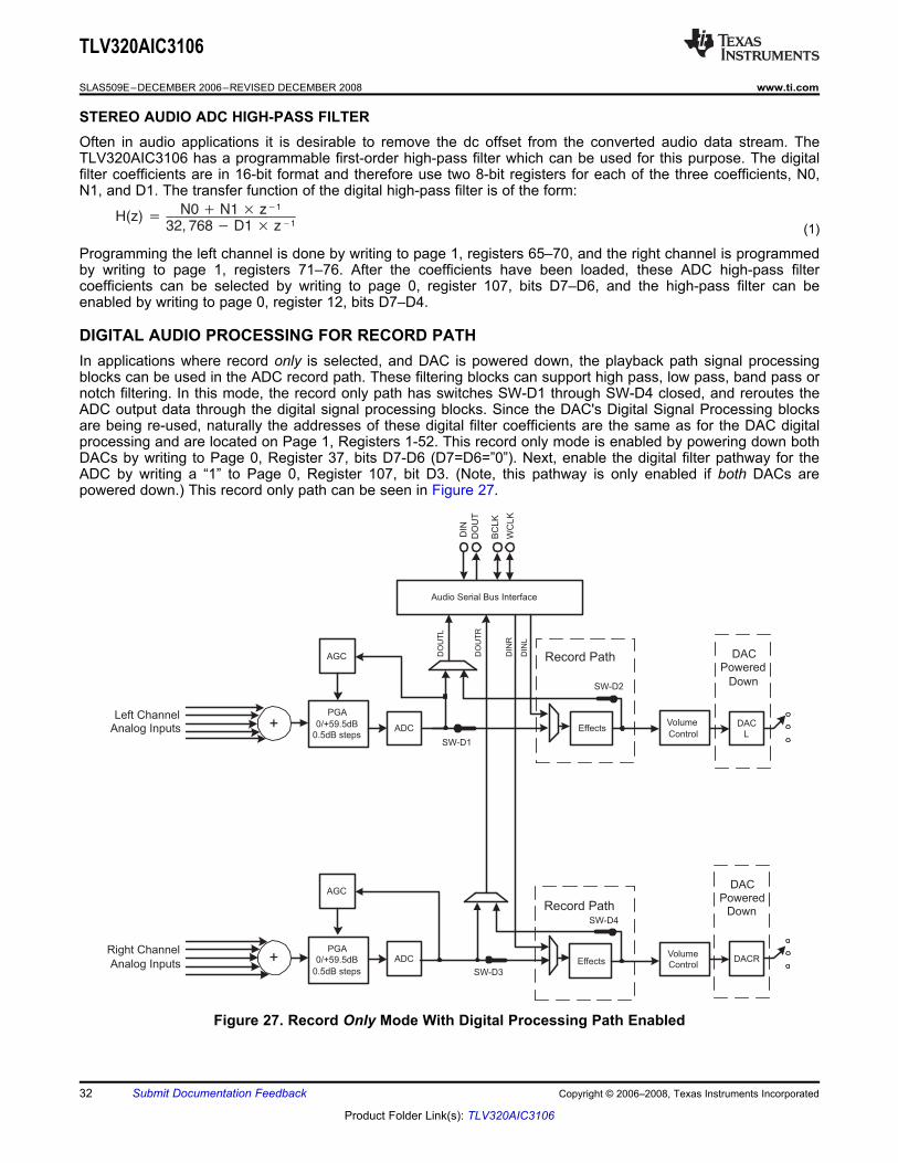
DIGITAL AUDIO PROCESSING FOR RECORD PATH
Audio�Serial�Bus�Interface
PGA
0/+59.5dB0.5dB�steps
ADC+ DACL
Volume
Control
DIN
DO
UT
BC
LK
WC
LK
DIN
L
DIN
R
DO
UT
L
DO
UT
R
ADCPGA
0/+59.5dB
0.5dB�steps
+ DACRVolumeControlEffects
AGC
AGC
Record�Path
Record�Path
DACPowered
Down
DACPowered
Down
Effects
SW-D1
SW-D2
SW-D3
SW-D4
Left�ChannelAnalog�Inputs
Right�ChannelAnalog�Inputs
TLV320AIC3106
SLAS509E–DECEMBER 2006–REVISED DECEMBER 2008........................................................................................................................................ www.ti.com
Often in audio applications it is desirable to remove the dc offset from the converted audio data stream. TheTLV320AIC3106 has a programmable first-order high-pass filter which can be used for this purpose. The digitalfilter coefficients are in 16-bit format and therefore use two 8-bit registers for each of the three coefficients, N0,N1, and D1. The transfer function of the digital high-pass filter is of the form:
Programming the left channel is done by writing to page 1, registers 65–70, and the right channel is programmedby writing to page 1, registers 71–76. After the coefficients have been loaded, these ADC high-pass filtercoefficients can be selected by writing to page 0, register 107, bits D7–D6, and the high-pass filter can beenabled by writing to page 0, register 12, bits D7–D4.
In applications where record only is selected, and DAC is powered down, the playback path signal processingblocks can be used in the ADC record path. These filtering blocks can support high pass, low pass, band pass ornotch filtering. In this mode, the record only path has switches SW-D1 through SW-D4 closed, and reroutes theADC output data through the digital signal processing blocks. Since the DAC's Digital Signal Processing blocksare being re-used, naturally the addresses of these digital filter coefficients are the same as for the DAC digitalprocessing and are located on Page 1, Registers 1-52. This record only mode is enabled by powering down bothDACs by writing to Page 0, Register 37, bits D7-D6 (D7=D6=”0”). Next, enable the digital filter pathway for theADC by writing a “1” to Page 0, Register 107, bit D3. (Note, this pathway is only enabled if both DACs arepowered down.) This record only path can be seen in Figure 27.
Figure 27. Record Only Mode With Digital Processing Path Enabled
32 Submit Documentation Feedback Copyright © 2006–2008, Texas Instruments Incorporated
Product Folder Link(s): TLV320AIC3106
AUTOMATIC GAIN CONTROL (AGC)
TLV320AIC3106
www.ti.com ........................................................................................................................................ SLAS509E–DECEMBER 2006–REVISED DECEMBER 2008
An automatic gain control (AGC) circuit is included with the ADC and can be used to maintain nominally constantoutput signal amplitude when recording speech signals (it can be fully disabled if not desired). This circuitryautomatically adjusts the PGA gain as the input signal becomes overly loud or very weak, such as when aperson speaking into a microphone moves closer or farther from the microphone. The AGC algorithm has severalprogrammable settings, including target gain, attack and decay time constants, noise threshold, and maximumPGA gain applicable that allow the algorithm to be fine tuned for any particular application. The algorithm usesthe absolute average of the signal (which is the average of the absolute value of the signal) as a measure of thenominal amplitude of the output signal.
Note that completely independent AGC circuitry is included with each ADC channel with entirely independentcontrol over the algorithm from one channel to the next. This is attractive in cases where two microphones areused in a system, but may have different placement in the end equipment and require different dynamicperformance for optimal system operation.
Target level represents the nominal output level at which the AGC attempts to hold the ADC output signal level.The TLV320AIC3106 allows programming of eight different target levels, which can be programmed from –5.5dB to –24 dB relative to a full-scale signal. Since the device reacts to the signal absolute average and not topeak levels, it is recommended that the target level be set with enough margin to avoid clipping at the occurrenceof loud sounds.
Attack time determines how quickly the AGC circuitry reduces the PGA gain when the input signal is too loud. Itcan be varied from 7 ms to 1,408 ms. The extended Right Channel Attack time can be programmed by writing toPage 0, Registers 103, and Left Channel is programmed by writing to Page 0, Register 105.
Decay time determines how quickly the PGA gain is increased when the input signal is too low. It can be variedin the range from 0.05 s to 22.4 s. The extended Right Channel Decay time can be programmed by writing toPage 0, Registers 104, and Left Channel is programmed by writing to Page 0, Register 106.
The actual AGC decay time maximum is based on a counter length, so the maximum decay time will scale withthe clock set up that is used. The table below shows the relationship of the NADC ratio to the maximum timeavailable for the AGC decay. In practice, these maximum times are extremely long for audio applications andshould not limit any practical AGC decay time that is needed by the system.
Table 1. AGC Decay Time RestrictionNADC RATIO MAXIMUM DECAY TIME (seconds)
1.0 4.01.5 5.62.0 8.02.5 9.63.0 11.23.5 11.24.0 16.04.5 16.05.0 19.25.5 22.46.0 22.4
Noise gate threshold determines the level below which if the input speech average value falls, AGC considers itas a silence and hence brings down the gain to 0 dB in steps of 0.5 dB every FS and sets the noise thresholdflag. The gain stays at 0 dB unless the input speech signal average rises above the noise threshold setting. Thisensures that noise does not get gained up in the absence of speech. Noise threshold level in the AGC algorithmis programmable from –30 dB to –90 dB relative to full scale. A disable noise gate feature is also available. Thisoperation includes programmable debounce and hysteresis functionality to avoid the AGC gain from cyclingbetween high gain and 0 dB when signals are near the noise threshold level. When the noise threshold flag isset, the status of gain applied by the AGC and the saturation flag should be ignored.
Copyright © 2006–2008, Texas Instruments Incorporated Submit Documentation Feedback 33
Product Folder Link(s): TLV320AIC3106

Decay Time
TargetLevel
InputSignal
OutputSignal
AGCGain
AttackTime
STEREO AUDIO DAC
TLV320AIC3106
SLAS509E–DECEMBER 2006–REVISED DECEMBER 2008........................................................................................................................................ www.ti.com
Maximum PGA gain applicable allows the user to restrict the maximum PGA gain that can be applied by theAGC algorithm. This can be used for limiting PGA gain in situations where environmental noise is greater thanprogrammed noise threshold. It can be programmed from 0 dB to 59.5 dB in steps of 0.5 dB.
Figure 28. Typical Operation of the AGC Algorithm During Speech Recording
Note that the time constants here are correct when the ADC is not in double-rate audio mode. The timeconstants are achieved using the fS(ref) value programmed in the control registers. However, if the fS(ref) is set inthe registers to, for example, 48 kHz, but the actual audio clock or PLL programming actually results in a differentfS(ref) in practice, then the time constants would not be correct.
The actual AGC decay time maximum is based on a counter length, so the maximum decay time scales with theclock set up that is used. Table 1 shows the relationship of the NADC ratio to the maximum time available for theAGC decay. In practice, these maximum times are extremely long for audio applications and should not limit anypractical AGC decay time that is needed by the system.
The TLV320AIC3106 includes a stereo audio DAC supporting sampling rates from 8 kHz to 96 kHz. Eachchannel of the stereo audio DAC consists of a digital audio processing block, a digital interpolation filter, multi-bitdigital delta-sigma modulator, and an analog reconstruction filter. The DAC is designed to provide enhancedperformance at low sampling rates through increased oversampling and image filtering, thereby keepingquantization noise generated within the delta-sigma modulator and signal images strongly suppressed within theaudio band to beyond 20 kHz. This is realized by keeping the upsampled rate constant at 128 × fS(ref) andchanging the oversampling ratio as the input sample rate is changed. For an fS(ref) of 48 kHz, the digitaldelta-sigma modulator always operates at a rate of 6.144 MHz. This ensures that quantization noise generatedwithin the delta-sigma modulator stays low within the frequency band below 20 kHz at all sample rates. Similarly,for an fS(ref) rate of 44.1 kHz, the digital delta-sigma modulator always operates at a rate of 5.6448 MHz.
The following restrictions apply in the case when the PLL is powered down and double-rate audio mode isenabled in the DAC.
Allowed Q values = 4, 8, 9, 12, 16Q values where equivalent fS(ref) can be achieved by turning on PLLQ = 5, 6, 7 (set P = 5 / 6 / 7 and K = 16.0 and PLL enabled)Q = 10, 14 (set P = 5, 7 and K = 8.0 and PLL enabled)
34 Submit Documentation Feedback Copyright © 2006–2008, Texas Instruments Incorporated
Product Folder Link(s): TLV320AIC3106
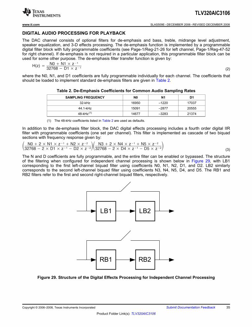
DIGITAL AUDIO PROCESSING FOR PLAYBACK
H(z) ! N0" N1# z$1
32768$ D1# z$1 (2)
! N0" 2# N1# z$1" N2# z$2
32768$ 2# D1# z$1$ D2# z$2%! N3" 2# N4# z$1" N5# z$2
32768$ 2# D4# z$1$ D5# z$2%
(3)
LB1 LB2
RB1 RB2
TLV320AIC3106
www.ti.com ........................................................................................................................................ SLAS509E–DECEMBER 2006–REVISED DECEMBER 2008
The DAC channel consists of optional filters for de-emphasis and bass, treble, midrange level adjustment,speaker equalization, and 3-D effects processing. The de-emphasis function is implemented by a programmabledigital filter block with fully programmable coefficients (see Page-1/Reg-21-26 for left channel, Page-1/Reg-47-52for right channel). If de-emphasis is not required in a particular application, this programmable filter block can beused for some other purpose. The de-emphasis filter transfer function is given by:
where the N0, N1, and D1 coefficients are fully programmable individually for each channel. The coefficients thatshould be loaded to implement standard de-emphasis filters are given in Table 2.
Table 2. De-Emphasis Coefficients for Common Audio Sampling RatesSAMPLING FREQUENCY N0 N1 D1
32-kHz 16950 –1220 1703744.1-kHz 15091 –2877 2055548-kHz(1) 14677 –3283 21374
(1) The 48-kHz coefficients listed in Table 2 are used as defaults.
In addition to the de-emphasis filter block, the DAC digital effects processing includes a fourth order digital IIRfilter with programmable coefficients (one set per channel). This filter is implemented as cascade of two biquadsections with frequency response given by:
The N and D coefficients are fully programmable, and the entire filter can be enabled or bypassed. The structureof the filtering when configured for independent channel processing is shown below in Figure 29, with LB1corresponding to the first left-channel biquad filter using coefficients N0, N1, N2, D1, and D2. LB2 similarlycorresponds to the second left-channel biquad filter using coefficients N3, N4, N5, D4, and D5. The RB1 andRB2 filters refer to the first and second right-channel biquad filters, respectively.
Figure 29. Structure of the Digital Effects Processing for Independent Channel Processing
Copyright © 2006–2008, Texas Instruments Incorporated Submit Documentation Feedback 35
Product Folder Link(s): TLV320AIC3106
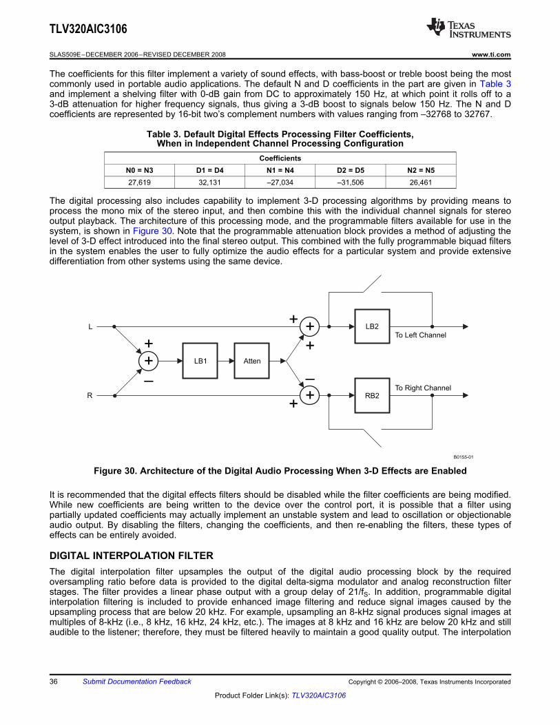
B0155-01
LB1
RB2
Atten
LB2L
+
+
+
+
+
––
+
+R
To�Left�Channel
To�Right�Channel
DIGITAL INTERPOLATION FILTER
TLV320AIC3106
SLAS509E–DECEMBER 2006–REVISED DECEMBER 2008........................................................................................................................................ www.ti.com
The coefficients for this filter implement a variety of sound effects, with bass-boost or treble boost being the mostcommonly used in portable audio applications. The default N and D coefficients in the part are given in Table 3and implement a shelving filter with 0-dB gain from DC to approximately 150 Hz, at which point it rolls off to a3-dB attenuation for higher frequency signals, thus giving a 3-dB boost to signals below 150 Hz. The N and Dcoefficients are represented by 16-bit two’s complement numbers with values ranging from –32768 to 32767.
Table 3. Default Digital Effects Processing Filter Coefficients,When in Independent Channel Processing Configuration
CoefficientsN0 = N3 D1 = D4 N1 = N4 D2 = D5 N2 = N527,619 32,131 –27,034 –31,506 26,461
The digital processing also includes capability to implement 3-D processing algorithms by providing means toprocess the mono mix of the stereo input, and then combine this with the individual channel signals for stereooutput playback. The architecture of this processing mode, and the programmable filters available for use in thesystem, is shown in Figure 30. Note that the programmable attenuation block provides a method of adjusting thelevel of 3-D effect introduced into the final stereo output. This combined with the fully programmable biquad filtersin the system enables the user to fully optimize the audio effects for a particular system and provide extensivedifferentiation from other systems using the same device.
Figure 30. Architecture of the Digital Audio Processing When 3-D Effects are Enabled
It is recommended that the digital effects filters should be disabled while the filter coefficients are being modified.While new coefficients are being written to the device over the control port, it is possible that a filter usingpartially updated coefficients may actually implement an unstable system and lead to oscillation or objectionableaudio output. By disabling the filters, changing the coefficients, and then re-enabling the filters, these types ofeffects can be entirely avoided.
The digital interpolation filter upsamples the output of the digital audio processing block by the requiredoversampling ratio before data is provided to the digital delta-sigma modulator and analog reconstruction filterstages. The filter provides a linear phase output with a group delay of 21/fS. In addition, programmable digitalinterpolation filtering is included to provide enhanced image filtering and reduce signal images caused by theupsampling process that are below 20 kHz. For example, upsampling an 8-kHz signal produces signal images atmultiples of 8-kHz (i.e., 8 kHz, 16 kHz, 24 kHz, etc.). The images at 8 kHz and 16 kHz are below 20 kHz and stillaudible to the listener; therefore, they must be filtered heavily to maintain a good quality output. The interpolation
36 Submit Documentation Feedback Copyright © 2006–2008, Texas Instruments Incorporated
Product Folder Link(s): TLV320AIC3106
DELTA-SIGMA AUDIO DAC
AUDIO DAC DIGITAL VOLUME CONTROL
INCREASING DAC DYNAMIC RANGE
ANALOG OUTPUT COMMON-MODE ADJUSTMENT
TLV320AIC3106
www.ti.com ........................................................................................................................................ SLAS509E–DECEMBER 2006–REVISED DECEMBER 2008
filter is designed to maintain at least 65-dB rejection of images that land below 7.455 fS. In order to utilize theprogrammable interpolation capability, the fS(ref) should be programmed to a higher rate (restricted to be in therange of 39 kHz to 53 kHz when the PLL is in use), and the actual fS is set using the NDAC divider. For example,if fS = 8 kHz is required, then fS(ref) can be set to 48 kHz, and the DAC fS set to fS(ref)/6. This ensures that allimages of the 8-kHz data are sufficiently attenuated well beyond a 20-kHz audible frequency range.
The stereo audio DAC incorporates a third order multi-bit delta-sigma modulator followed by an analogreconstruction filter. The DAC provides high-resolution, low-noise performance, using oversampling and noiseshaping techniques. The analog reconstruction filter design consists of a 6-tap analog FIR filter followed by acontinuous time RC filter. The analog FIR operates at a rate of 128 × fS(ref) (6.144 MHz when fS(ref) = 48 kHz,5.6448 MHz when fS(ref) = 44.1 kHz). Note that the DAC analog performance may be degraded by excessiveclock jitter on the MCLK input. Therefore, care must be taken to keep jitter on this clock to a minimum.
The audio DAC includes a digital volume control block which implements a programmable digital gain. Thevolume level can be varied from 0 dB to –63.5 dB in 0.5-dB steps, in addition to a mute bit, independently foreach channel. The volume level of both channels can also be changed simultaneously by the master volumecontrol. Gain changes are implemented with a soft-stepping algorithm, which only changes the actual volume byone step per input sample, either up or down, until the desired volume is reached. The rate of soft-stepping canbe slowed to one step per two input samples through a register bit.
Because of soft-stepping, the host does not know when the DAC has been actually muted. This may beimportant if the host wishes to mute the DAC before making a significant change, such as changing samplerates. In order to help with this situation, the device provides a flag back to the host via a read-only register bitthat alerts the host when the part has completed the soft-stepping and the actual volume has reached thedesired volume level. The soft-stepping feature can be disabled through register programming. If soft-stepping isenabled, the MCLK signal should be kept applied to the device until the DAC power-down flag is set. When thisflag is set, the internal soft-stepping process and power down sequence is complete, and the MCLK can then bestopped if desired.
The TLV320AIC3106 also includes functionality to detect when the user switches on or off the de-emphasis ordigital audio processing functions, to first (1) soft-mute the DAC volume control, (2) change the operation of thedigital effects processing, and (3) soft-unmute the part. This avoids any possible pop/clicks in the audio outputdue to instantaneous changes in the filtering. A similar algorithm is used when first powering up or down theDAC. The circuit begins operation at power up with the volume control muted, then soft-steps it up to the desiredvolume level. At power down, the logic first soft-steps the volume down to a mute level, then powers down thecircuitry.
The TLV320AIC3106 allows trading off dynamic range with power consumption. The DAC dynamic range can beincreased by writing to Page 0, Register 109 bits D7-D6. The lowest DAC current setting is the default, and thedynamic range is displayed in the datasheet table. Increasing the current can increase the DAC dynamic rangeby up to 1.5dB.
The output common-mode voltage and output range of the analog output are determined by an internal bandgapreference, in contrast to other codecs that may use a divided version of the supply. This scheme is used toreduce the coupling of noise that may be on the supply (such as 217-Hz noise in a GSM cellphone) into theaudio signal path.
However, due to the possible wide variation in analog supply range (2.7 V – 3.6 V), an output common-modevoltage setting of 1.35 V, which would be used for a 2.7 V supply case, will be overly conservative if the supply isactually much larger, such as 3.3 V or 3.6 V. In order to optimize device operation, the TLV320AIC3106 includes
Copyright © 2006–2008, Texas Instruments Incorporated Submit Documentation Feedback 37
Product Folder Link(s): TLV320AIC3106
AUDIO DAC POWER CONTROL
AUDIO ANALOG INPUTS
TLV320AIC3106
SLAS509E–DECEMBER 2006–REVISED DECEMBER 2008........................................................................................................................................ www.ti.com
a programmable output common-mode level, which can be set by register programming to a level mostappropriate to the actual supply range used by a particular customer. The output common-mode level can bevaried among four different values, ranging from 1.35 V (most appropriate for low supply ranges, near 2.7 V) to1.8 V (most appropriate for high supply ranges, near 3.6 V). Note that there is also some limitation on the rangeof DVDD voltage as well in determining which setting is most appropriate.
Table 4. Appropriate SettingsCM SETTING RECOMMENDED AVDD_DAC, RECOMMENDED DVDD
DRVDD1.35 2.7 V – 3.6 V 1.65 V – 1.95 V1.50 3.0 V – 3.6 V 1.65 V – 1.95 V1.65 V 3.3 V – 3.6 V 1.8 V – 1.95 V1.8 V 3.6 V 1.95 V
The stereo DAC can be fully powered up or down, and in addition, the analog circuitry in each DAC channel canbe powered up or down independently. This provides power savings when only a mono playback stream isneeded.
The TLV320AIC3106 includes ten analog audio input pins, which can be configured as up to four fully-differentialpair plus one single-ended pair of audio inputs, or up to six single-ended audio inputs. . These pins connectthrough series resistors and switches to the virtual ground terminals of two fully differential opamps (one perADC/PGA channel). By selecting to turn on only one set of switches per opamp at a time, the inputs can beeffectively muxed to each ADC PGA channel.
By selecting to turn on multiple sets of switches per opamp at a time, mixing can also be achieved. Mixing ofmultiple inputs can easily lead to PGA outputs that exceed the range of the internal opamps, resulting insaturation and clipping of the mixed output signal. Whenever mixing is being implemented, the user should takeadequate precautions to avoid such a saturation case from occurring. In general, the mixed signal should notexceed 2 Vpp (single-ended) or 4 Vpp (differential).
In most mixing applications, there is also a general need to adjust the levels of the individual signals beingmixed. For example, if a soft signal and a large signal are to be mixed and played together, the soft signalgenerally should be amplified to a level comparable to the large signal before mixing. In order to accommodatethis need, the TLV320AIC3106 includes input level control on each of the individual inputs before they are mixedor muxed into the ADC PGAs, with gain programmable from 0 dB to –12 dB in 1.5 dB steps. Note that this inputlevel control is not intended to be a volume control, but instead used occasionally for level setting. Soft-steppingof the input level control settings is implemented in this device, with the speed and functionality following thesettings used by the ADC PGA for soft-stepping.
The TLV320AIC3106 supports the ability to mix up to three fully-differential analog inputs into each ADC PGAchannel. Figure 31 shows the mixing configuration for the left channel, which can mix the signalsLINE1LP-LINE1LM, LINE2LP-LINE2LM, and LINE1RP-LINE1RM
38 Submit Documentation Feedback Copyright © 2006–2008, Texas Instruments Incorporated
Product Folder Link(s): TLV320AIC3106

GAIN=0,−1.5,−3,..,−12dB,MUTE
LINE1LP
LINE1LM
LINE2LP
LINE2LM
LINE1RP
LINE1RM
TO LEFT ADCPGA
GAIN=0,−1.5,−3,..,−12dB, MUTE
GAIN=0,−1.5,−3,..,−12dB,MUTE
TLV320AIC3106
www.ti.com ........................................................................................................................................ SLAS509E–DECEMBER 2006–REVISED DECEMBER 2008
Figure 31. Left Channel Fully-Differential Analog Input Mixing Configuration
Three fully-differential analog inputs can similarly be mixed into the right ADC PGA as well, consisting ofLINE1RP-LINE1RM, LINE2RP-LINE2RM, and LINE1LP-LINE1LM. Note that it is not necessary to mix all threefully-differential signals if this is not desired – unnecessary inputs can simply be muted using the input levelcontrol registers.
Copyright © 2006–2008, Texas Instruments Incorporated Submit Documentation Feedback 39
Product Folder Link(s): TLV320AIC3106
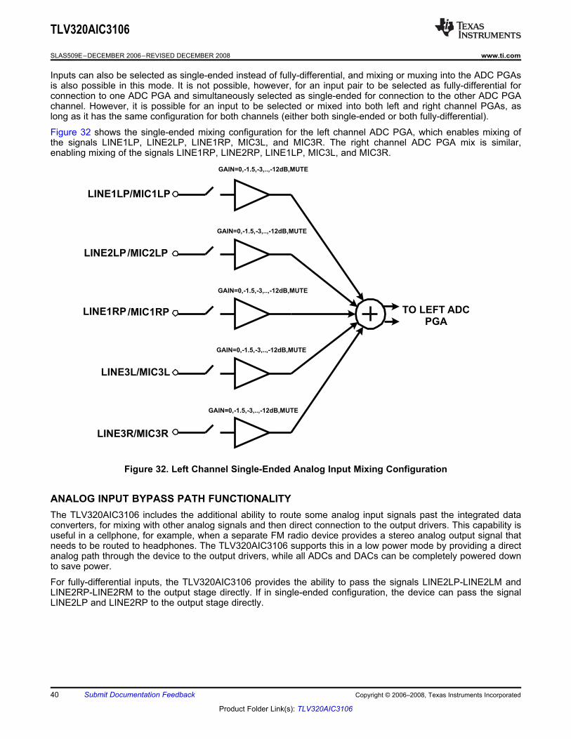
GAIN=0,-1.5,-3,..,-12dB,MUTE
LINE1LP/MIC1LP
LINE2LP/MIC2LP
LINE1RP/MIC1RP
LINE3L/MIC3L
LINE3R/MIC3R
GAIN=0,-1.5,-3,..,-12dB,MUTE
GAIN=0,-1.5,-3,..,-12dB,MUTE
GAIN=0,-1.5,-3,..,-12dB,MUTE
GAIN=0,-1.5,-3,..,-12dB,MUTE
TO�LEFT ADCPGA
ANALOG INPUT BYPASS PATH FUNCTIONALITY
TLV320AIC3106
SLAS509E–DECEMBER 2006–REVISED DECEMBER 2008........................................................................................................................................ www.ti.com
Inputs can also be selected as single-ended instead of fully-differential, and mixing or muxing into the ADC PGAsis also possible in this mode. It is not possible, however, for an input pair to be selected as fully-differential forconnection to one ADC PGA and simultaneously selected as single-ended for connection to the other ADC PGAchannel. However, it is possible for an input to be selected or mixed into both left and right channel PGAs, aslong as it has the same configuration for both channels (either both single-ended or both fully-differential).
Figure 32 shows the single-ended mixing configuration for the left channel ADC PGA, which enables mixing ofthe signals LINE1LP, LINE2LP, LINE1RP, MIC3L, and MIC3R. The right channel ADC PGA mix is similar,enabling mixing of the signals LINE1RP, LINE2RP, LINE1LP, MIC3L, and MIC3R.
Figure 32. Left Channel Single-Ended Analog Input Mixing Configuration
The TLV320AIC3106 includes the additional ability to route some analog input signals past the integrated dataconverters, for mixing with other analog signals and then direct connection to the output drivers. This capability isuseful in a cellphone, for example, when a separate FM radio device provides a stereo analog output signal thatneeds to be routed to headphones. The TLV320AIC3106 supports this in a low power mode by providing a directanalog path through the device to the output drivers, while all ADCs and DACs can be completely powered downto save power.
For fully-differential inputs, the TLV320AIC3106 provides the ability to pass the signals LINE2LP-LINE2LM andLINE2RP-LINE2RM to the output stage directly. If in single-ended configuration, the device can pass the signalLINE2LP and LINE2RP to the output stage directly.
40 Submit Documentation Feedback Copyright © 2006–2008, Texas Instruments Incorporated
Product Folder Link(s): TLV320AIC3106
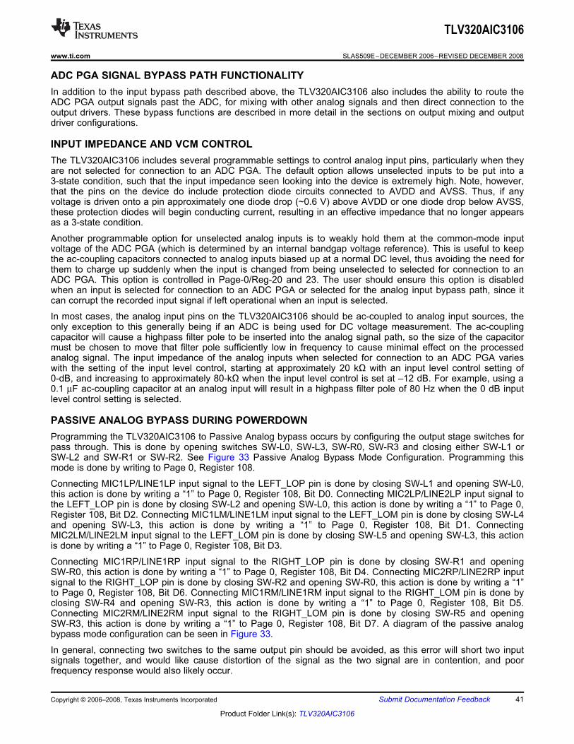
ADC PGA SIGNAL BYPASS PATH FUNCTIONALITY
INPUT IMPEDANCE AND VCM CONTROL
PASSIVE ANALOG BYPASS DURING POWERDOWN
TLV320AIC3106
www.ti.com ........................................................................................................................................ SLAS509E–DECEMBER 2006–REVISED DECEMBER 2008
In addition to the input bypass path described above, the TLV320AIC3106 also includes the ability to route theADC PGA output signals past the ADC, for mixing with other analog signals and then direct connection to theoutput drivers. These bypass functions are described in more detail in the sections on output mixing and outputdriver configurations.
The TLV320AIC3106 includes several programmable settings to control analog input pins, particularly when theyare not selected for connection to an ADC PGA. The default option allows unselected inputs to be put into a3-state condition, such that the input impedance seen looking into the device is extremely high. Note, however,that the pins on the device do include protection diode circuits connected to AVDD and AVSS. Thus, if anyvoltage is driven onto a pin approximately one diode drop (~0.6 V) above AVDD or one diode drop below AVSS,these protection diodes will begin conducting current, resulting in an effective impedance that no longer appearsas a 3-state condition.
Another programmable option for unselected analog inputs is to weakly hold them at the common-mode inputvoltage of the ADC PGA (which is determined by an internal bandgap voltage reference). This is useful to keepthe ac-coupling capacitors connected to analog inputs biased up at a normal DC level, thus avoiding the need forthem to charge up suddenly when the input is changed from being unselected to selected for connection to anADC PGA. This option is controlled in Page-0/Reg-20 and 23. The user should ensure this option is disabledwhen an input is selected for connection to an ADC PGA or selected for the analog input bypass path, since itcan corrupt the recorded input signal if left operational when an input is selected.
In most cases, the analog input pins on the TLV320AIC3106 should be ac-coupled to analog input sources, theonly exception to this generally being if an ADC is being used for DC voltage measurement. The ac-couplingcapacitor will cause a highpass filter pole to be inserted into the analog signal path, so the size of the capacitormust be chosen to move that filter pole sufficiently low in frequency to cause minimal effect on the processedanalog signal. The input impedance of the analog inputs when selected for connection to an ADC PGA varieswith the setting of the input level control, starting at approximately 20 k� with an input level control setting of0-dB, and increasing to approximately 80-k� when the input level control is set at –12 dB. For example, using a0.1 µF ac-coupling capacitor at an analog input will result in a highpass filter pole of 80 Hz when the 0 dB inputlevel control setting is selected.
Programming the TLV320AIC3106 to Passive Analog bypass occurs by configuring the output stage switches forpass through. This is done by opening switches SW-L0, SW-L3, SW-R0, SW-R3 and closing either SW-L1 orSW-L2 and SW-R1 or SW-R2. See Figure 33 Passive Analog Bypass Mode Configuration. Programming thismode is done by writing to Page 0, Register 108.
Connecting MIC1LP/LINE1LP input signal to the LEFT_LOP pin is done by closing SW-L1 and opening SW-L0,this action is done by writing a “1” to Page 0, Register 108, Bit D0. Connecting MIC2LP/LINE2LP input signal tothe LEFT_LOP pin is done by closing SW-L2 and opening SW-L0, this action is done by writing a “1” to Page 0,Register 108, Bit D2. Connecting MIC1LM/LINE1LM input signal to the LEFT_LOM pin is done by closing SW-L4and opening SW-L3, this action is done by writing a “1” to Page 0, Register 108, Bit D1. ConnectingMIC2LM/LINE2LM input signal to the LEFT_LOM pin is done by closing SW-L5 and opening SW-L3, this actionis done by writing a “1” to Page 0, Register 108, Bit D3.
Connecting MIC1RP/LINE1RP input signal to the RIGHT_LOP pin is done by closing SW-R1 and openingSW-R0, this action is done by writing a “1” to Page 0, Register 108, Bit D4. Connecting MIC2RP/LINE2RP inputsignal to the RIGHT_LOP pin is done by closing SW-R2 and opening SW-R0, this action is done by writing a “1”to Page 0, Register 108, Bit D6. Connecting MIC1RM/LINE1RM input signal to the RIGHT_LOM pin is done byclosing SW-R4 and opening SW-R3, this action is done by writing a “1” to Page 0, Register 108, Bit D5.Connecting MIC2RM/LINE2RM input signal to the RIGHT_LOM pin is done by closing SW-R5 and openingSW-R3, this action is done by writing a “1” to Page 0, Register 108, Bit D7. A diagram of the passive analogbypass mode configuration can be seen in Figure 33.
In general, connecting two switches to the same output pin should be avoided, as this error will short two inputsignals together, and would like cause distortion of the signal as the two signal are in contention, and poorfrequency response would also likely occur.
Copyright © 2006–2008, Texas Instruments Incorporated Submit Documentation Feedback 41
Product Folder Link(s): TLV320AIC3106
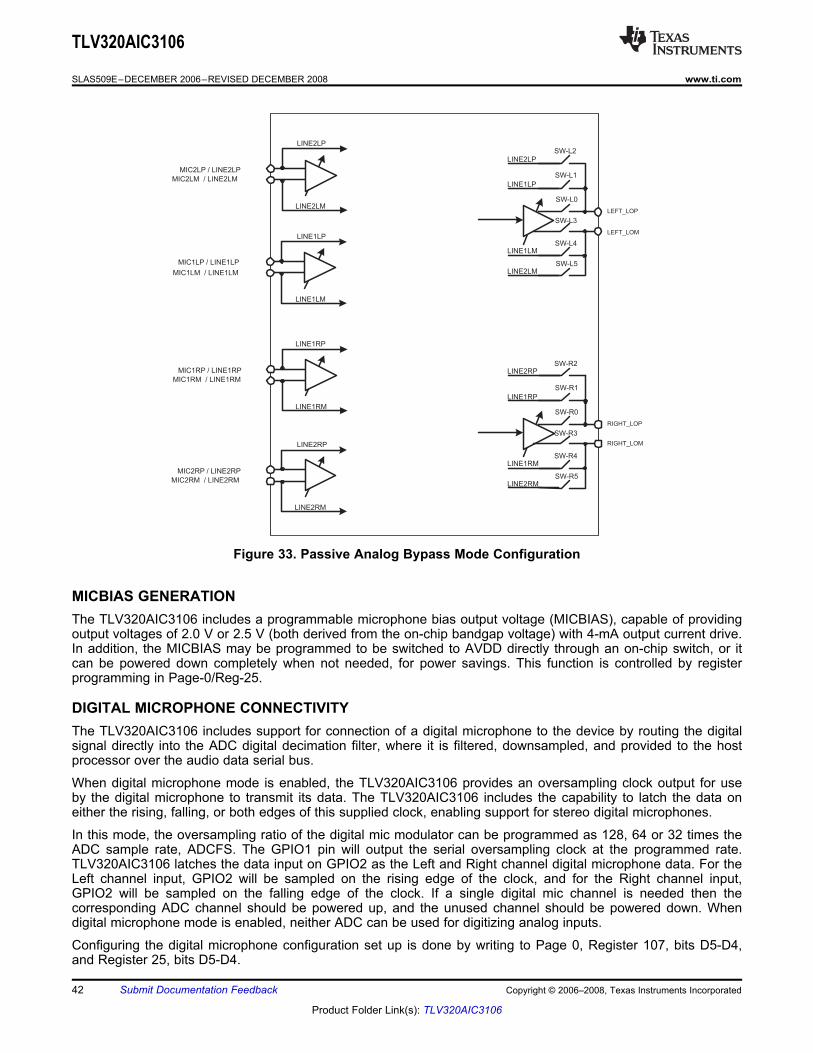
MIC2RM��/�LINE2RM
MIC2RP /�LINE2RP
LINE2RP
LINE2RM
MIC1RM��/�LINE1RM
MIC1RP /�LINE1RP
LINE1RP
LINE1RM
MIC1LM��/�LINE1LM
MIC1LP /�LINE1LP
LINE1LP
LINE1LM
MIC2LM��/�LINE2LM
MIC2LP /�LINE2LP
LINE2LP
LINE2LM
LINE1LP
LINE2LM
LINE2LP
LINE1LM
SW-L0
SW-L3
SW-L1
SW-L2
SW-L4
SW-L5
LINE1RP
LINE2RM
LINE2RP
LINE1RM
SW-R0
SW-R3
SW-R1
SW-R2
SW-R4
SW-R5
RIGHT_LOP
RIGHT_LOM
LEFT_LOP
LEFT_LOM
MICBIAS GENERATION
DIGITAL MICROPHONE CONNECTIVITY
TLV320AIC3106
SLAS509E–DECEMBER 2006–REVISED DECEMBER 2008........................................................................................................................................ www.ti.com
Figure 33. Passive Analog Bypass Mode Configuration
The TLV320AIC3106 includes a programmable microphone bias output voltage (MICBIAS), capable of providingoutput voltages of 2.0 V or 2.5 V (both derived from the on-chip bandgap voltage) with 4-mA output current drive.In addition, the MICBIAS may be programmed to be switched to AVDD directly through an on-chip switch, or itcan be powered down completely when not needed, for power savings. This function is controlled by registerprogramming in Page-0/Reg-25.
The TLV320AIC3106 includes support for connection of a digital microphone to the device by routing the digitalsignal directly into the ADC digital decimation filter, where it is filtered, downsampled, and provided to the hostprocessor over the audio data serial bus.
When digital microphone mode is enabled, the TLV320AIC3106 provides an oversampling clock output for useby the digital microphone to transmit its data. The TLV320AIC3106 includes the capability to latch the data oneither the rising, falling, or both edges of this supplied clock, enabling support for stereo digital microphones.
In this mode, the oversampling ratio of the digital mic modulator can be programmed as 128, 64 or 32 times theADC sample rate, ADCFS. The GPIO1 pin will output the serial oversampling clock at the programmed rate.TLV320AIC3106 latches the data input on GPIO2 as the Left and Right channel digital microphone data. For theLeft channel input, GPIO2 will be sampled on the rising edge of the clock, and for the Right channel input,GPIO2 will be sampled on the falling edge of the clock. If a single digital mic channel is needed then thecorresponding ADC channel should be powered up, and the unused channel should be powered down. Whendigital microphone mode is enabled, neither ADC can be used for digitizing analog inputs.
Configuring the digital microphone configuration set up is done by writing to Page 0, Register 107, bits D5-D4,and Register 25, bits D5-D4.
42 Submit Documentation Feedback Copyright © 2006–2008, Texas Instruments Incorporated
Product Folder Link(s): TLV320AIC3106
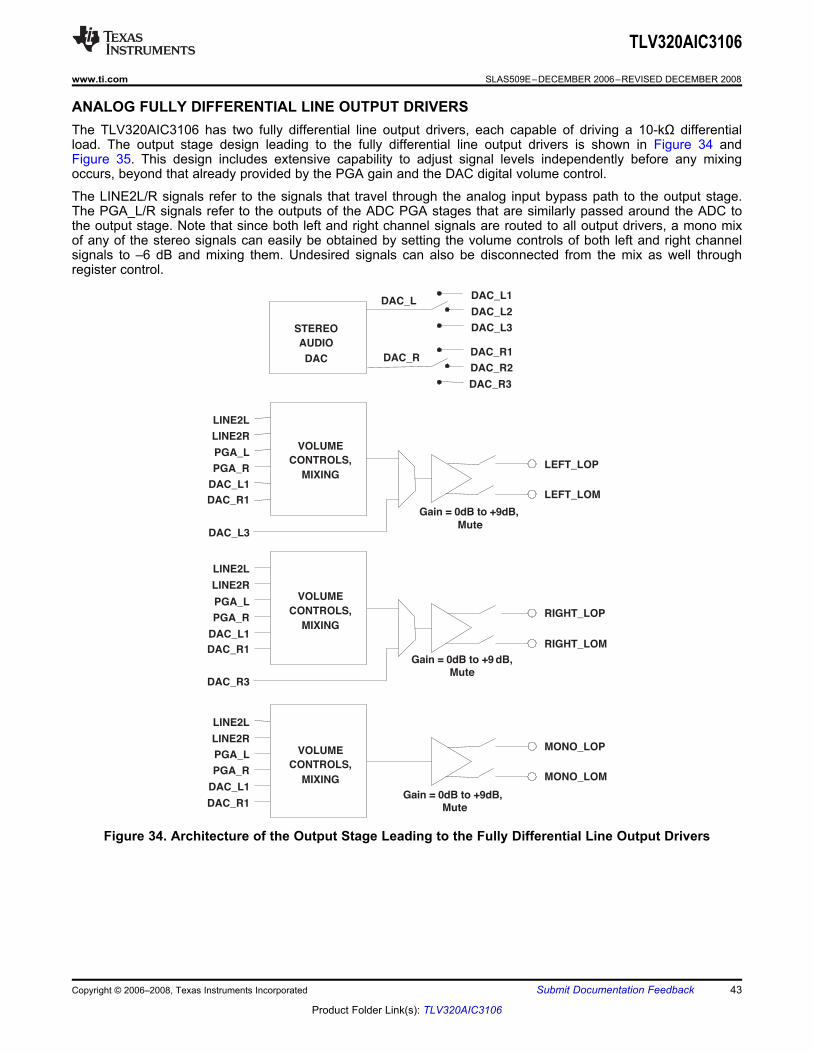
ANALOG FULLY DIFFERENTIAL LINE OUTPUT DRIVERS
VOLUMECONTROLS,
MIXING
LINE2LLINE2RPGA_LPGA_R
DAC_L1DAC_R1
DAC_L3
LEFT_LOP
LEFT_LOMGain = 0dB to +9dB,
Mute
LINE2LLINE2RPGA_LPGA_R
DAC_L1DAC_R1
DAC_R3
RIGHT_LOP
RIGHT_LOMGain = 0dB to +9 dB,
Mute
LINE2LLINE2RPGA_LPGA_R
DAC_L1DAC_R1
MONO_LOP
MONO_LOMGain = 0dB to +9dB,
Mute
DAC_L DAC_L1DAC_L2DAC_L3
DAC_R DAC_R1DAC_R2DAC_R3
STEREOAUDIODAC
VOLUMECONTROLS,
MIXING
VOLUMECONTROLS,
MIXING
TLV320AIC3106
www.ti.com ........................................................................................................................................ SLAS509E–DECEMBER 2006–REVISED DECEMBER 2008
The TLV320AIC3106 has two fully differential line output drivers, each capable of driving a 10-k� differentialload. The output stage design leading to the fully differential line output drivers is shown in Figure 34 andFigure 35. This design includes extensive capability to adjust signal levels independently before any mixingoccurs, beyond that already provided by the PGA gain and the DAC digital volume control.
The LINE2L/R signals refer to the signals that travel through the analog input bypass path to the output stage.The PGA_L/R signals refer to the outputs of the ADC PGA stages that are similarly passed around the ADC tothe output stage. Note that since both left and right channel signals are routed to all output drivers, a mono mixof any of the stereo signals can easily be obtained by setting the volume controls of both left and right channelsignals to –6 dB and mixing them. Undesired signals can also be disconnected from the mix as well throughregister control.
Figure 34. Architecture of the Output Stage Leading to the Fully Differential Line Output Drivers
Copyright © 2006–2008, Texas Instruments Incorporated Submit Documentation Feedback 43
Product Folder Link(s): TLV320AIC3106

0dB�to -78dB
0dB�to -78dB
0dB�to -78dB
0dB�to -78dB
0dB�to -78dB
0dB�to -78dB
+
LINE2L/MIC2L
LINE2R/MIC2R
PGA_L
PGA_R
DAC_L1
DAC_R1
ANALOG HIGH POWER OUTPUT DRIVERS
TLV320AIC3106
SLAS509E–DECEMBER 2006–REVISED DECEMBER 2008........................................................................................................................................ www.ti.com
Figure 35. Detail of the Volume Control and Mixing Function Shown in Figure 29 and Figure 17
The DAC_L/R signals are the outputs of the stereo audio DAC, which can be steered by register control basedon the requirements of the system. If mixing of the DAC audio with other signals is not required, and the DACoutput is only needed at the stereo line outputs, then it is recommended to use the routing through pathDAC_L3/R3 to the fully differential stereo line outputs. This results not only in higher quality output performance,but also in lower power operation, since the analog volume controls and mixing blocks ahead of these driverscan be powered down.
If instead the DAC analog output must be routed to multiple output drivers simultaneously (such as toLEFT_LOP/M, RIGHT_LOP/M, and MONO_LOP/M) or must be mixed with other analog signals, then the DACoutputs should be switched through the DAC_L1/R1 path. This option provides the maximum flexibility for routingof the DAC analog signals to the output drivers
The TLV320AIC3106 includes an output level control on each output driver with limited gain adjustment from 0dB to 9 dB. The output driver circuitry in this device are designed to provide a low distortion output while playingfullscale stereo DAC signals at a 0dB gain setting. However, a higher amplitude output can be obtained at thecost of increased signal distortion at the output. This output level control allows the user to make this tradeoffbased on the requirements of the end equipment. Note that this output level control is not intended to be used asa standard output volume control. It is expected to be used only sparingly for level setting, i.e., adjustment of thefullscale output range of the device.
Each differential line output driver can be powered down independently of the others when it is not needed in thesystem. When placed into powerdown through register programming, the driver output pins will be placed into a3-stated, high-impedance state.
The TLV320AIC3106 includes four high power output drivers with extensive flexibility in their usage. Theseoutput drivers are individually capable of driving 30 mW each into a 16-� load in single-ended configuration, andthey can be used in pairs connected in bridge-terminated load (BTL) configuration between two driver outputs.
The high power output drivers can be configured in a variety of ways, including:1. driving up to two fully differential output signals2. driving up to four single-ended output signals3. driving two single-ended output signals, with one or two of the remaining drivers driving a fixed VCM level,for a pseudo-differential stereo output
44 Submit Documentation Feedback Copyright © 2006–2008, Texas Instruments Incorporated
Product Folder Link(s): TLV320AIC3106
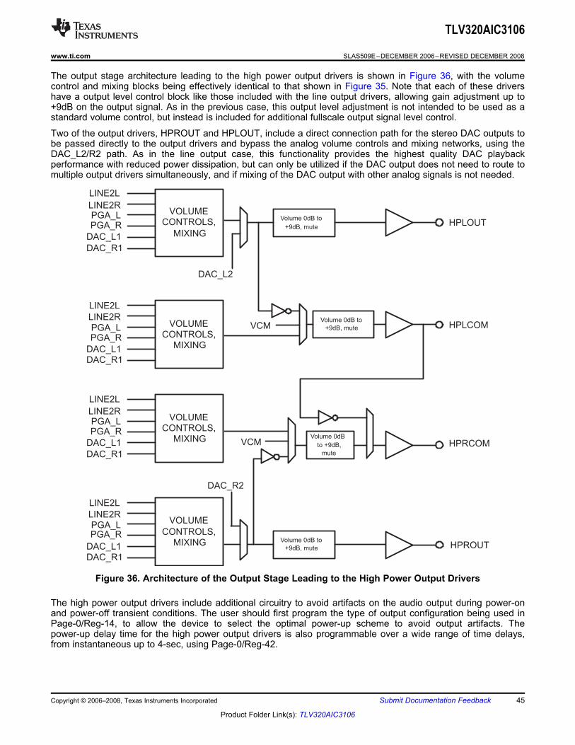
Volume�0dB�to
+9dB,�mute
Volume�0dB�to
+9dB,�muteVCM
Volume�0dB�to
+9dB,�mute
Volume�0dB
to�+9dB,
mute
VCM
HPLOUT
HPLCOM
HPROUT
HPRCOM
DAC_L2
LINE2L
LINE2RPGA_L
DAC_L1DAC_R1
VOLUMECONTROLS,
MIXINGPGA_R
DAC_R2
LINE2LLINE2RPGA_L
DAC_L1DAC_R1
VOLUMECONTROLS,
MIXINGPGA_R
LINE2L
LINE2RPGA_L
DAC_L1DAC_R1
VOLUMECONTROLS,
MIXINGPGA_R
LINE2LLINE2RPGA_L
DAC_L1DAC_R1
VOLUMECONTROLS,
MIXINGPGA_R
TLV320AIC3106
www.ti.com ........................................................................................................................................ SLAS509E–DECEMBER 2006–REVISED DECEMBER 2008
The output stage architecture leading to the high power output drivers is shown in Figure 36, with the volumecontrol and mixing blocks being effectively identical to that shown in Figure 35. Note that each of these drivershave a output level control block like those included with the line output drivers, allowing gain adjustment up to+9dB on the output signal. As in the previous case, this output level adjustment is not intended to be used as astandard volume control, but instead is included for additional fullscale output signal level control.
Two of the output drivers, HPROUT and HPLOUT, include a direct connection path for the stereo DAC outputs tobe passed directly to the output drivers and bypass the analog volume controls and mixing networks, using theDAC_L2/R2 path. As in the line output case, this functionality provides the highest quality DAC playbackperformance with reduced power dissipation, but can only be utilized if the DAC output does not need to route tomultiple output drivers simultaneously, and if mixing of the DAC output with other analog signals is not needed.
Figure 36. Architecture of the Output Stage Leading to the High Power Output Drivers
The high power output drivers include additional circuitry to avoid artifacts on the audio output during power-onand power-off transient conditions. The user should first program the type of output configuration being used inPage-0/Reg-14, to allow the device to select the optimal power-up scheme to avoid output artifacts. Thepower-up delay time for the high power output drivers is also programmable over a wide range of time delays,from instantaneous up to 4-sec, using Page-0/Reg-42.
Copyright © 2006–2008, Texas Instruments Incorporated Submit Documentation Feedback 45
Product Folder Link(s): TLV320AIC3106
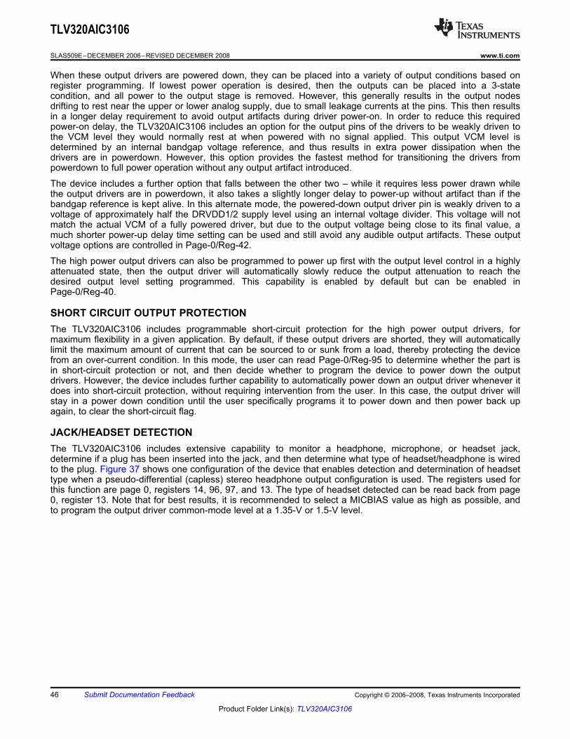
SHORT CIRCUIT OUTPUT PROTECTION
JACK/HEADSET DETECTION
TLV320AIC3106
SLAS509E–DECEMBER 2006–REVISED DECEMBER 2008........................................................................................................................................ www.ti.com
When these output drivers are powered down, they can be placed into a variety of output conditions based onregister programming. If lowest power operation is desired, then the outputs can be placed into a 3-statecondition, and all power to the output stage is removed. However, this generally results in the output nodesdrifting to rest near the upper or lower analog supply, due to small leakage currents at the pins. This then resultsin a longer delay requirement to avoid output artifacts during driver power-on. In order to reduce this requiredpower-on delay, the TLV320AIC3106 includes an option for the output pins of the drivers to be weakly driven tothe VCM level they would normally rest at when powered with no signal applied. This output VCM level isdetermined by an internal bandgap voltage reference, and thus results in extra power dissipation when thedrivers are in powerdown. However, this option provides the fastest method for transitioning the drivers frompowerdown to full power operation without any output artifact introduced.
The device includes a further option that falls between the other two – while it requires less power drawn whilethe output drivers are in powerdown, it also takes a slightly longer delay to power-up without artifact than if thebandgap reference is kept alive. In this alternate mode, the powered-down output driver pin is weakly driven to avoltage of approximately half the DRVDD1/2 supply level using an internal voltage divider. This voltage will notmatch the actual VCM of a fully powered driver, but due to the output voltage being close to its final value, amuch shorter power-up delay time setting can be used and still avoid any audible output artifacts. These outputvoltage options are controlled in Page-0/Reg-42.
The high power output drivers can also be programmed to power up first with the output level control in a highlyattenuated state, then the output driver will automatically slowly reduce the output attenuation to reach thedesired output level setting programmed. This capability is enabled by default but can be enabled inPage-0/Reg-40.
The TLV320AIC3106 includes programmable short-circuit protection for the high power output drivers, formaximum flexibility in a given application. By default, if these output drivers are shorted, they will automaticallylimit the maximum amount of current that can be sourced to or sunk from a load, thereby protecting the devicefrom an over-current condition. In this mode, the user can read Page-0/Reg-95 to determine whether the part isin short-circuit protection or not, and then decide whether to program the device to power down the outputdrivers. However, the device includes further capability to automatically power down an output driver whenever itdoes into short-circuit protection, without requiring intervention from the user. In this case, the output driver willstay in a power down condition until the user specifically programs it to power down and then power back upagain, to clear the short-circuit flag.
The TLV320AIC3106 includes extensive capability to monitor a headphone, microphone, or headset jack,determine if a plug has been inserted into the jack, and then determine what type of headset/headphone is wiredto the plug. Figure 37 shows one configuration of the device that enables detection and determination of headsettype when a pseudo-differential (capless) stereo headphone output configuration is used. The registers used forthis function are page 0, registers 14, 96, 97, and 13. The type of headset detected can be read back from page0, register 13. Note that for best results, it is recommended to select a MICBIAS value as high as possible, andto program the output driver common-mode level at a 1.35-V or 1.5-V level.
46 Submit Documentation Feedback Copyright © 2006–2008, Texas Instruments Incorporated
Product Folder Link(s): TLV320AIC3106
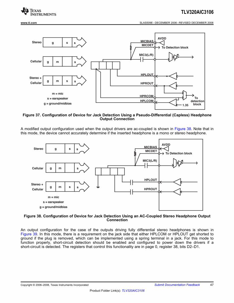
MICBIAS
MIC3(L/R)
HPLOUT
HPROUT
Todetection
block
HPRCOMHPLCOM
1.35
MICDETTo Detection block
s
sg m
sg m s
sgStereo
Cellular
Stereo +Cellular
m = mics = earspeaker
g = ground/midbias
AVDD
MICBIAS
MIC3(L/R)
HPLOUT
HPROUT
MICDETTo Detection block
s
sg m
sg m s
sgStereo
Cellular
Stereo +Cellular
m = mics = earspeaker
g = ground/midbias
AVDD
TLV320AIC3106
www.ti.com ........................................................................................................................................ SLAS509E–DECEMBER 2006–REVISED DECEMBER 2008
Figure 37. Configuration of Device for Jack Detection Using a Pseudo-Differential (Capless) HeadphoneOutput Connection
A modified output configuration used when the output drivers are ac-coupled is shown in Figure 38. Note that inthis mode, the device cannot accurately determine if the inserted headphone is a mono or stereo headphone.
Figure 38. Configuration of Device for Jack Detection Using an AC-Coupled Stereo Headphone OutputConnection
An output configuration for the case of the outputs driving fully differential stereo headphones is shown inFigure 39. In this mode, there is a requirement on the jack side that either HPLCOM or HPLOUT get shorted toground if the plug is removed, which can be implemented using a spring terminal in a jack. For this mode tofunction properly, short-circuit detection should be enabled and configured to power down the drivers if ashort-circuit is detected. The registers that control this functionality are in page 0, register 38, bits D2–D1.
Copyright © 2006–2008, Texas Instruments Incorporated Submit Documentation Feedback 47
Product Folder Link(s): TLV320AIC3106

To Detection block
HPLOUT
HPLCOM
HPROUT
HPRCOM
MICDETThis switch closes when
jack is removed
GENERAL-PURPOSE I/O
CONTROL REGISTERS
TLV320AIC3106
SLAS509E–DECEMBER 2006–REVISED DECEMBER 2008........................................................................................................................................ www.ti.com
Figure 39. Configuration of Device for Jack Detection Using a Fully Differential Stereo Headphone OutputConnection
TLV320AIC3106 has two dedicated pins for general-purpose I/O. These pins can be used to read status ofexternal signals through register read when configured as general-purpose input. When configured asgeneral-purpose output , these pins can also drive logic high or low. Besides these standard GPIO functions,these pins can also be used in a variety of ways, such as output for internal clocks and interrupt signals. TheTLV320AIC3106 generates a variety of interrupts of use to the host processor such interrupts on jack detection,button press, short-circuit detection, and AGC noise detection. All these interrupts can be routed individually tothe GPIO pins or can be combined by a logical OR. In case of a combined interrupt, the user can read aninternal status register to find the actual cause of interrupt. When configured as interrupt, the TLV320AIC3106also offers the flexibility of generating a single pulse or a train of pulses until the interrupt status register is readby the user.
The control registers for the TLV320AIC3106 are described in detail below. All registers are 8 bit in width, withD7 referring to the most significant bit of each register, and D0 referring to the least significant bit.
Page 0 / Register 0: Page Select RegisterREAD/ RESETBIT(1) DESCRIPTIONWRITE VALUE
D7–D1 X 0000 000 Reserved, write only zeros to these register bitsD0 R/W 0 Page Select Bit
Writing zero to this bit sets Page-0 as the active page for following register accesses. Writing a one to thisbit sets Page-1 as the active page for following register accesses. It is recommended that the user readthis register bit back after each write, to ensure that the proper page is being accessed for future registerread/writes.
(1) When resetting registers related to routing and volume controls of output drivers, it is recommended to reset them by writing directly tothe registers instead of using software reset.
48 Submit Documentation Feedback Copyright © 2006–2008, Texas Instruments Incorporated
Product Folder Link(s): TLV320AIC3106
TLV320AIC3106
www.ti.com ........................................................................................................................................ SLAS509E–DECEMBER 2006–REVISED DECEMBER 2008
Page 0 / Register 1: Software Reset RegisterREAD/ RESETBIT DESCRIPTIONWRITE VALUE
D7 W 0 Software Reset Bit0 : Don’t Care1 : Self clearing software reset
D6–D0 W 000 0000 Reserved; don’t write
Page 0 / Register 2: Codec Sample Rate Select RegisterREAD/ RESETBIT DESCRIPTIONWRITE VALUE
D7–D4 R/W 0000 ADC Sample Rate Select0000: ADC fS = fS(ref)/10001: ADC fS = fS(ref)/1.50010: ADC fS = fS(ref)/20011: ADC fS = fS(ref)/2.50100: ADC fS = fS(ref)/30101: ADC fS = fS(ref)/3.50110: ADC fS = fS(ref)/40111: ADC fS = fS(ref)/4.51000: ADC fS = fS(ref)/51001: ADC fS = fS(ref)/5.51010: ADC fS = fS(ref)/61011–1111: Reserved, do not write these sequences.
D3–D0 R/W 0000 DAC Sample Rate Select0000 : DAC fS = fS(ref)/10001 : DAC fS = fS(ref)/1.50010 : DAC fS = fS(ref)/20011 : DAC fS = fS(ref)/2.50100 : DAC fS = fS(ref)/30101 : DAC fS = fS(ref)/3.50110 : DAC fS = fS(ref)/40111 : DAC fS = fS(ref)/4.51000 : DAC fS = fS(ref)/51001: DAC fS = fS(ref)/5.51010: DAC fS = fS(ref) / 61011–1111 : Reserved, do not write these sequences.
Page 0 / Register 3: PLL Programming Register AREAD/ RESETBIT DESCRIPTIONWRITE VALUE
D7 R/W 0 PLL Control Bit0: PLL is disabled1: PLL is enabled
D6–D3 R/W 0010 PLL Q Value0000: Q = 160001 : Q = 170010 : Q = 20011 : Q = 30100 : Q = 4…1110: Q = 141111: Q = 15
D2–D0 R/W 000 PLL P Value000: P = 8001: P = 1010: P = 2011: P = 3100: P = 4101: P = 5110: P = 6111: P = 7
Copyright © 2006–2008, Texas Instruments Incorporated Submit Documentation Feedback 49
Product Folder Link(s): TLV320AIC3106
TLV320AIC3106
SLAS509E–DECEMBER 2006–REVISED DECEMBER 2008........................................................................................................................................ www.ti.com
Page 0 / Register 4: PLL Programming Register BREAD/ RESETBIT DESCRIPTIONWRITE VALUE
D7–D2 R/W 0000 01 PLL J Value0000 00: Reserved, do not write this sequence0000 01: J = 10000 10: J = 20000 11: J = 3…1111 10: J = 621111 11: J = 63
D1–D0 R/W 00 Reserved, write only zeros to these bits
Page 0 / Register 5: PLL Programming Register C(1)READ/ RESETBIT DESCRIPTIONWRITE VALUE
D7–D0 R/W 0000 0000 PLL D value – Eight most significant bits of a 14-bit unsigned integer valid values for D are from zero to9999, represented by a 14-bit integer located in Page-0/Reg-5-6. Values should not be written into theseregisters that would result in a D value outside the valid range.
(1) Note that whenever the D value is changed, register 5 should be written, immediately followed by register 6. Even if only the MSB orLSB of the value changes, both registers should be written.
Page 0 / Register 6: PLL Programming Register DREAD/ RESETBIT DESCRIPTIONWRITE VALUE
D7–D2 R/W 0000 0000 PLL D value – Six least significant bits of a 14-bit unsigned integer valid values for D are from zero to9999, represented by a 14-bit integer located in Page-0/Reg-5-6. Values should not be written into theseregisters that would result in a D value outside the valid range.
D1–D0 R 00 Reserved, write only zeros to these bits.
Page 0 / Register 7: Codec Datapath Setup RegisterREAD/ RESETBIT DESCRIPTIONWRITE VALUE
D7 R/W 0 fS(ref) settingThis register setting controls timers related to the AGC time constants.0: fS(ref) = 48 kHz1: fS(ref) = 44.1 kHz
D6 R/W 0 ADC Dual rate control0: ADC dual rate mode is disabled1: ADC dual rate mode is enabledNote: ADC Dual Rate Mode must match DAC Dual Rate Mode
D5 R/W 0 DAC Dual Rate Control0: DAC dual rate mode is disabled1: DAC dual rate mode is enabled
D4–D3 R/W 00 Left DAC Datapath Control00: Left DAC datapath is off (muted)01: Left DAC datapath plays left channel input data10: Left DAC datapath plays right channel input data11: Left DAC datapath plays mono mix of left and right channel input data
D2–D1 R/W 00 Right DAC Datapath Control00: Right DAC datapath is off (muted)01: Right DAC datapath plays right channel input data10: Right DAC datapath plays left channel input data11: Right DAC datapath plays mono mix of left and right channel input data
D0 R/W 0 Reserved. Only write zero to this register.
50 Submit Documentation Feedback Copyright © 2006–2008, Texas Instruments Incorporated
Product Folder Link(s): TLV320AIC3106
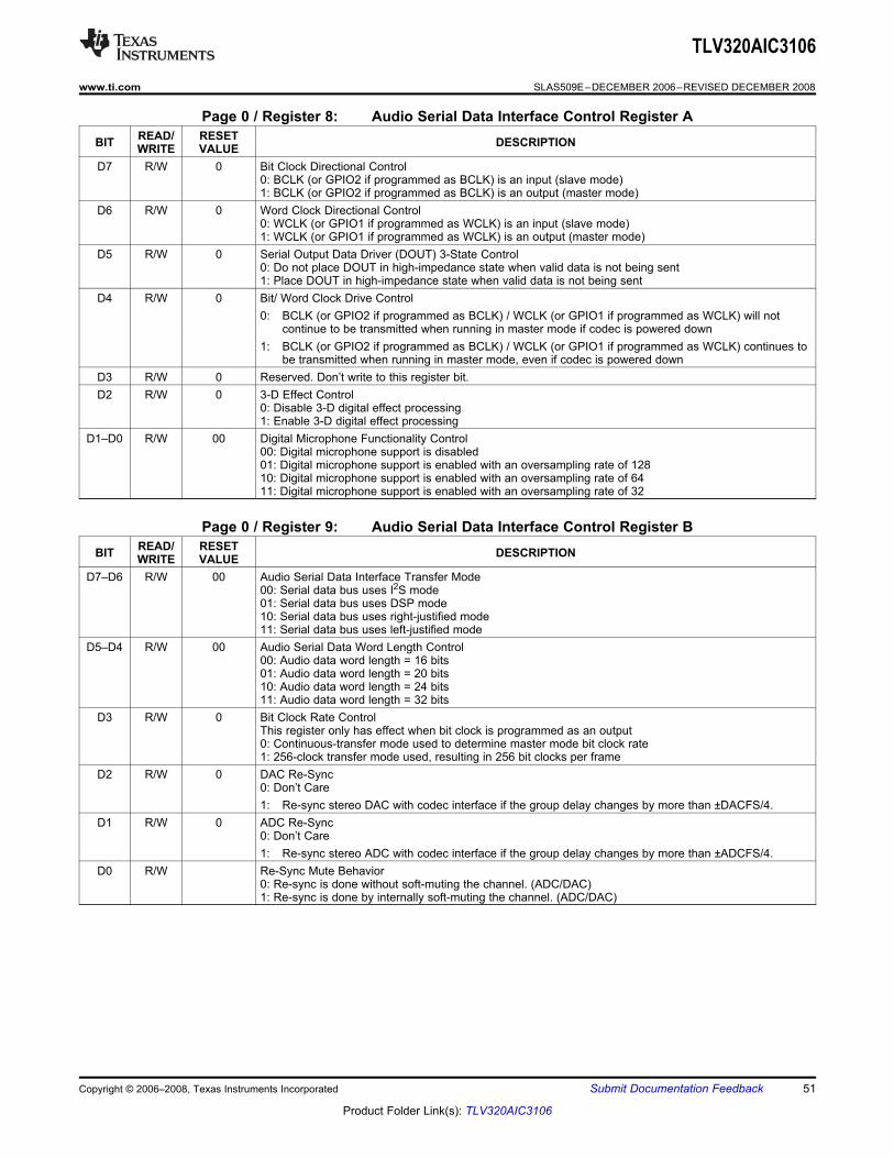
TLV320AIC3106
www.ti.com ........................................................................................................................................ SLAS509E–DECEMBER 2006–REVISED DECEMBER 2008
Page 0 / Register 8: Audio Serial Data Interface Control Register AREAD/ RESETBIT DESCRIPTIONWRITE VALUE
D7 R/W 0 Bit Clock Directional Control0: BCLK (or GPIO2 if programmed as BCLK) is an input (slave mode)1: BCLK (or GPIO2 if programmed as BCLK) is an output (master mode)
D6 R/W 0 Word Clock Directional Control0: WCLK (or GPIO1 if programmed as WCLK) is an input (slave mode)1: WCLK (or GPIO1 if programmed as WCLK) is an output (master mode)
D5 R/W 0 Serial Output Data Driver (DOUT) 3-State Control0: Do not place DOUT in high-impedance state when valid data is not being sent1: Place DOUT in high-impedance state when valid data is not being sent
D4 R/W 0 Bit/ Word Clock Drive Control0: BCLK (or GPIO2 if programmed as BCLK) / WCLK (or GPIO1 if programmed as WCLK) will not
continue to be transmitted when running in master mode if codec is powered down1: BCLK (or GPIO2 if programmed as BCLK) / WCLK (or GPIO1 if programmed as WCLK) continues to
be transmitted when running in master mode, even if codec is powered downD3 R/W 0 Reserved. Don’t write to this register bit.D2 R/W 0 3-D Effect Control
0: Disable 3-D digital effect processing1: Enable 3-D digital effect processing
D1–D0 R/W 00 Digital Microphone Functionality Control00: Digital microphone support is disabled01: Digital microphone support is enabled with an oversampling rate of 12810: Digital microphone support is enabled with an oversampling rate of 6411: Digital microphone support is enabled with an oversampling rate of 32
Page 0 / Register 9: Audio Serial Data Interface Control Register BREAD/ RESETBIT DESCRIPTIONWRITE VALUE
D7–D6 R/W 00 Audio Serial Data Interface Transfer Mode00: Serial data bus uses I2S mode01: Serial data bus uses DSP mode10: Serial data bus uses right-justified mode11: Serial data bus uses left-justified mode
D5–D4 R/W 00 Audio Serial Data Word Length Control00: Audio data word length = 16 bits01: Audio data word length = 20 bits10: Audio data word length = 24 bits11: Audio data word length = 32 bits
D3 R/W 0 Bit Clock Rate ControlThis register only has effect when bit clock is programmed as an output0: Continuous-transfer mode used to determine master mode bit clock rate1: 256-clock transfer mode used, resulting in 256 bit clocks per frame
D2 R/W 0 DAC Re-Sync0: Don’t Care1: Re-sync stereo DAC with codec interface if the group delay changes by more than ±DACFS/4.
D1 R/W 0 ADC Re-Sync0: Don’t Care1: Re-sync stereo ADC with codec interface if the group delay changes by more than ±ADCFS/4.
D0 R/W Re-Sync Mute Behavior0: Re-sync is done without soft-muting the channel. (ADC/DAC)1: Re-sync is done by internally soft-muting the channel. (ADC/DAC)
Copyright © 2006–2008, Texas Instruments Incorporated Submit Documentation Feedback 51
Product Folder Link(s): TLV320AIC3106

TLV320AIC3106
SLAS509E–DECEMBER 2006–REVISED DECEMBER 2008........................................................................................................................................ www.ti.com
Page 0 / Register 10: Audio Serial Data Interface Control Register CREAD/ RESETBIT DESCRIPTIONWRITE VALUE
D7–D0 R/W 0000 0000 Audio Serial Data Word Offset ControlThis register determines where valid data is placed or expected in each frame, by controlling the offsetfrom beginning of the frame where valid data begins. The offset is measured from the rising edge of wordclock when in DSP mode.0000 0000: Data offset = 0 bit clocks0000 0001: Data offset = 1 bit clock0000 0010: Data offset = 2 bit clocks…Note: In continuous transfer mode the maximum offset is 17 for I2S/LJF/RJF modes and 16 for DSPmode. In 256-clock mode, the maximum offset is 242 for I2S/LJF/RJF and 241 for DSP modes.1111 1110: Data offset = 254 bit clocks1111 1111: Data offset = 255 bit clocks
Page 0 / Register 11: Audio Codec Overflow Flag RegisterREAD/ RESETBIT DESCRIPTIONWRITE VALUE
D7 R 0 Left ADC Overflow FlagThis is a sticky bit, so will stay set if an overflow occurs, even if the overflow condition is removed. Theregister bit reset to 0 after it is read.0: No overflow has occurred1: An overflow has occurred
D6 R 0 Right ADC Overflow FlagThis is a sticky bit, so will stay set if an overflow occurs, even if the overflow condition is removed. Theregister bit reset to 0 after it is read.0: No overflow has occurred1: An overflow has occurred
D5 R 0 Left DAC Overflow FlagThis is a sticky bit, so will stay set if an overflow occurs, even if the overflow condition is removed. Theregister bit reset to 0 after it is read.0: No overflow has occurred1: An overflow has occurred
D4 R 0 Right DAC Overflow FlagThis is a sticky bit, so will stay set if an overflow occurs, even if the overflow condition is removed. Theregister bit reset to 0 after it is read.0: No overflow has occurred1: An overflow has occurred
D3–D0 R/W 0001 PLL R Value0000: R = 160001 : R = 10010 : R = 20011 : R = 30100 : R = 4…1110: R = 141111: R = 15
52 Submit Documentation Feedback Copyright © 2006–2008, Texas Instruments Incorporated
Product Folder Link(s): TLV320AIC3106
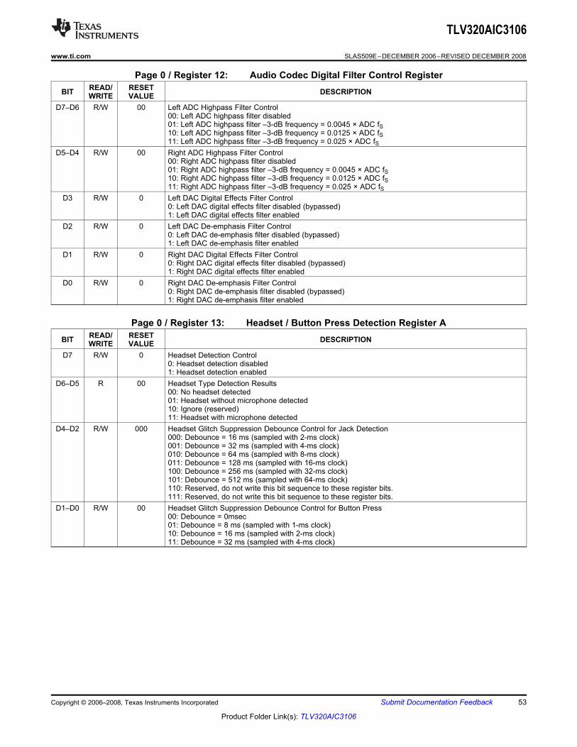
TLV320AIC3106
www.ti.com ........................................................................................................................................ SLAS509E–DECEMBER 2006–REVISED DECEMBER 2008
Page 0 / Register 12: Audio Codec Digital Filter Control RegisterREAD/ RESETBIT DESCRIPTIONWRITE VALUE
D7–D6 R/W 00 Left ADC Highpass Filter Control00: Left ADC highpass filter disabled01: Left ADC highpass filter –3-dB frequency = 0.0045 × ADC fS10: Left ADC highpass filter –3-dB frequency = 0.0125 × ADC fS11: Left ADC highpass filter –3-dB frequency = 0.025 × ADC fS
D5–D4 R/W 00 Right ADC Highpass Filter Control00: Right ADC highpass filter disabled01: Right ADC highpass filter –3-dB frequency = 0.0045 × ADC fS10: Right ADC highpass filter –3-dB frequency = 0.0125 × ADC fS11: Right ADC highpass filter –3-dB frequency = 0.025 × ADC fS
D3 R/W 0 Left DAC Digital Effects Filter Control0: Left DAC digital effects filter disabled (bypassed)1: Left DAC digital effects filter enabled
D2 R/W 0 Left DAC De-emphasis Filter Control0: Left DAC de-emphasis filter disabled (bypassed)1: Left DAC de-emphasis filter enabled
D1 R/W 0 Right DAC Digital Effects Filter Control0: Right DAC digital effects filter disabled (bypassed)1: Right DAC digital effects filter enabled
D0 R/W 0 Right DAC De-emphasis Filter Control0: Right DAC de-emphasis filter disabled (bypassed)1: Right DAC de-emphasis filter enabled
Page 0 / Register 13: Headset / Button Press Detection Register AREAD/ RESETBIT DESCRIPTIONWRITE VALUE
D7 R/W 0 Headset Detection Control0: Headset detection disabled1: Headset detection enabled
D6–D5 R 00 Headset Type Detection Results00: No headset detected01: Headset without microphone detected10: Ignore (reserved)11: Headset with microphone detected
D4–D2 R/W 000 Headset Glitch Suppression Debounce Control for Jack Detection000: Debounce = 16 ms (sampled with 2-ms clock)001: Debounce = 32 ms (sampled with 4-ms clock)010: Debounce = 64 ms (sampled with 8-ms clock)011: Debounce = 128 ms (sampled with 16-ms clock)100: Debounce = 256 ms (sampled with 32-ms clock)101: Debounce = 512 ms (sampled with 64-ms clock)110: Reserved, do not write this bit sequence to these register bits.111: Reserved, do not write this bit sequence to these register bits.
D1–D0 R/W 00 Headset Glitch Suppression Debounce Control for Button Press00: Debounce = 0msec01: Debounce = 8 ms (sampled with 1-ms clock)10: Debounce = 16 ms (sampled with 2-ms clock)11: Debounce = 32 ms (sampled with 4-ms clock)
Copyright © 2006–2008, Texas Instruments Incorporated Submit Documentation Feedback 53
Product Folder Link(s): TLV320AIC3106
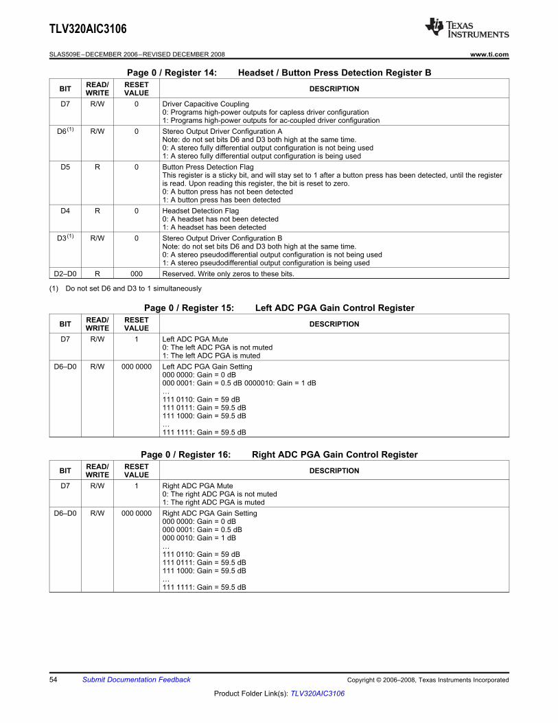
TLV320AIC3106
SLAS509E–DECEMBER 2006–REVISED DECEMBER 2008........................................................................................................................................ www.ti.com
Page 0 / Register 14: Headset / Button Press Detection Register BREAD/ RESETBIT DESCRIPTIONWRITE VALUE
D7 R/W 0 Driver Capacitive Coupling0: Programs high-power outputs for capless driver configuration1: Programs high-power outputs for ac-coupled driver configuration
D6(1) R/W 0 Stereo Output Driver Configuration ANote: do not set bits D6 and D3 both high at the same time.0: A stereo fully differential output configuration is not being used1: A stereo fully differential output configuration is being used
D5 R 0 Button Press Detection FlagThis register is a sticky bit, and will stay set to 1 after a button press has been detected, until the registeris read. Upon reading this register, the bit is reset to zero.0: A button press has not been detected1: A button press has been detected
D4 R 0 Headset Detection Flag0: A headset has not been detected1: A headset has been detected
D3(1) R/W 0 Stereo Output Driver Configuration BNote: do not set bits D6 and D3 both high at the same time.0: A stereo pseudodifferential output configuration is not being used1: A stereo pseudodifferential output configuration is being used
D2–D0 R 000 Reserved. Write only zeros to these bits.
(1) Do not set D6 and D3 to 1 simultaneously
Page 0 / Register 15: Left ADC PGA Gain Control RegisterREAD/ RESETBIT DESCRIPTIONWRITE VALUE
D7 R/W 1 Left ADC PGA Mute0: The left ADC PGA is not muted1: The left ADC PGA is muted
D6–D0 R/W 000 0000 Left ADC PGA Gain Setting000 0000: Gain = 0 dB000 0001: Gain = 0.5 dB 0000010: Gain = 1 dB…111 0110: Gain = 59 dB111 0111: Gain = 59.5 dB111 1000: Gain = 59.5 dB…111 1111: Gain = 59.5 dB
Page 0 / Register 16: Right ADC PGA Gain Control RegisterREAD/ RESETBIT DESCRIPTIONWRITE VALUE
D7 R/W 1 Right ADC PGA Mute0: The right ADC PGA is not muted1: The right ADC PGA is muted
D6–D0 R/W 000 0000 Right ADC PGA Gain Setting000 0000: Gain = 0 dB000 0001: Gain = 0.5 dB000 0010: Gain = 1 dB…111 0110: Gain = 59 dB111 0111: Gain = 59.5 dB111 1000: Gain = 59.5 dB…111 1111: Gain = 59.5 dB
54 Submit Documentation Feedback Copyright © 2006–2008, Texas Instruments Incorporated
Product Folder Link(s): TLV320AIC3106
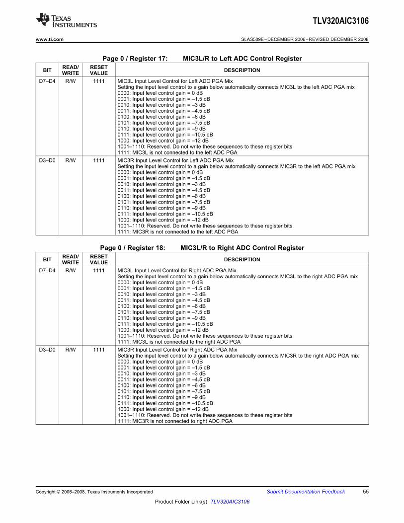
TLV320AIC3106
www.ti.com ........................................................................................................................................ SLAS509E–DECEMBER 2006–REVISED DECEMBER 2008
Page 0 / Register 17: MIC3L/R to Left ADC Control RegisterREAD/ RESETBIT DESCRIPTIONWRITE VALUE
D7–D4 R/W 1111 MIC3L Input Level Control for Left ADC PGA MixSetting the input level control to a gain below automatically connects MIC3L to the left ADC PGA mix0000: Input level control gain = 0 dB0001: Input level control gain = –1.5 dB0010: Input level control gain = –3 dB0011: Input level control gain = –4.5 dB0100: Input level control gain = –6 dB0101: Input level control gain = –7.5 dB0110: Input level control gain = –9 dB0111: Input level control gain = –10.5 dB1000: Input level control gain = –12 dB1001–1110: Reserved. Do not write these sequences to these register bits1111: MIC3L is not connected to the left ADC PGA
D3–D0 R/W 1111 MIC3R Input Level Control for Left ADC PGA MixSetting the input level control to a gain below automatically connects MIC3R to the left ADC PGA mix0000: Input level control gain = 0 dB0001: Input level control gain = –1.5 dB0010: Input level control gain = –3 dB0011: Input level control gain = –4.5 dB0100: Input level control gain = –6 dB0101: Input level control gain = –7.5 dB0110: Input level control gain = –9 dB0111: Input level control gain = –10.5 dB1000: Input level control gain = –12 dB1001–1110: Reserved. Do not write these sequences to these register bits1111: MIC3R is not connected to the left ADC PGA
Page 0 / Register 18: MIC3L/R to Right ADC Control RegisterREAD/ RESETBIT DESCRIPTIONWRITE VALUE
D7–D4 R/W 1111 MIC3L Input Level Control for Right ADC PGA MixSetting the input level control to a gain below automatically connects MIC3L to the right ADC PGA mix0000: Input level control gain = 0 dB0001: Input level control gain = –1.5 dB0010: Input level control gain = –3 dB0011: Input level control gain = –4.5 dB0100: Input level control gain = –6 dB0101: Input level control gain = –7.5 dB0110: Input level control gain = –9 dB0111: Input level control gain = –10.5 dB1000: Input level control gain = –12 dB1001–1110: Reserved. Do not write these sequences to these register bits1111: MIC3L is not connected to the right ADC PGA
D3–D0 R/W 1111 MIC3R Input Level Control for Right ADC PGA MixSetting the input level control to a gain below automatically connects MIC3R to the right ADC PGA mix0000: Input level control gain = 0 dB0001: Input level control gain = –1.5 dB0010: Input level control gain = –3 dB0011: Input level control gain = –4.5 dB0100: Input level control gain = –6 dB0101: Input level control gain = –7.5 dB0110: Input level control gain = –9 dB0111: Input level control gain = –10.5 dB1000: Input level control gain = –12 dB1001–1110: Reserved. Do not write these sequences to these register bits1111: MIC3R is not connected to right ADC PGA
Copyright © 2006–2008, Texas Instruments Incorporated Submit Documentation Feedback 55
Product Folder Link(s): TLV320AIC3106
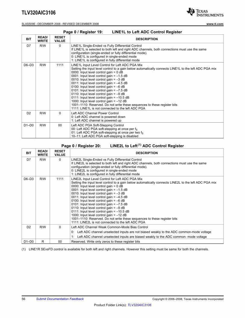
TLV320AIC3106
SLAS509E–DECEMBER 2006–REVISED DECEMBER 2008........................................................................................................................................ www.ti.com
Page 0 / Register 19: LINE1L to Left ADC Control RegisterREAD/ RESETBIT DESCRIPTIONWRITE VALUE
D7 R/W 0 LINE1L Single-Ended vs Fully Differential ControlIf LINE1L is selected to both left and right ADC channels, both connections must use the sameconfiguration (single-ended or fully differential mode).0: LINE1L is configured in single-ended mode1: LINE1L is configured in fully differential mode
D6–D3 R/W 1111 LINE1L Input Level Control for Left ADC PGA MixSetting the input level control to a gain below automatically connects LINE1L to the left ADC PGA mix0000: Input level control gain = 0 dB0001: Input level control gain = –1.5 dB0010: Input level control gain = –3 dB0011: Input level control gain = –4.5 dB0100: Input level control gain = –6 dB0101: Input level control gain = –7.5 dB0110: Input level control gain = –9 dB0111: Input level control gain = –10.5 dB1000: Input level control gain = –12 dB1001–1110: Reserved. Do not write these sequences to these register bits1111: LINE1L is not connected to the left ADC PGA
D2 R/W 0 Left ADC Channel Power Control0: Left ADC channel is powered down1: Left ADC channel is powered up
D1–D0 R/W 00 Left ADC PGA Soft-Stepping Control00: Left ADC PGA soft-stepping at once per fS01: Left ADC PGA soft-stepping at once per two fS10–11: Left ADC PGA soft-stepping is disabled
Page 0 / Register 20: LINE2L to Left(1) ADC Control RegisterREAD/ RESETBIT DESCRIPTIONWRITE VALUE
D7 R/W 0 LINE2L Single-Ended vs Fully Differential ControlIf LINE2L is selected to both left and right ADC channels, both connections must use the sameconfiguration (single-ended or fully differential mode).0: LINE2L is configured in single-ended mode1: LINE2L is configured in fully differential mode
D6–D3 R/W 1111 LINE2L Input Level Control for Left ADC PGA MixSetting the input level control to a gain below automatically connects LINE2L to the left ADC PGA mix0000: Input level control gain = 0 dB0001: Input level control gain = –1.5 dB0010: Input level control gain = –3 dB0011: Input level control gain = –4.5 dB0100: Input level control gain = –6 dB0101: Input level control gain = –7.5 dB0110: Input level control gain = –9 dB0111: Input level control gain = –10.5 dB1000: Input level control gain = –12 dB1001–1110: Reserved. Do not write these sequences to these register bits1111: LINE2L is not connected to the left ADC PGA
D2 R/W 0 Left ADC Channel Weak Common-Mode Bias Control0: Left ADC channel unselected inputs are not biased weakly to the ADC common-mode voltage1: Left ADC channel unselected inputs are biased weakly to the ADC common- mode voltage
D1–D0 R 00 Reserved. Write only zeros to these register bits
(1) LINE1R SEvsFD control is available for both left and right channels. However this setting must be same for both the channels.
56 Submit Documentation Feedback Copyright © 2006–2008, Texas Instruments Incorporated
Product Folder Link(s): TLV320AIC3106
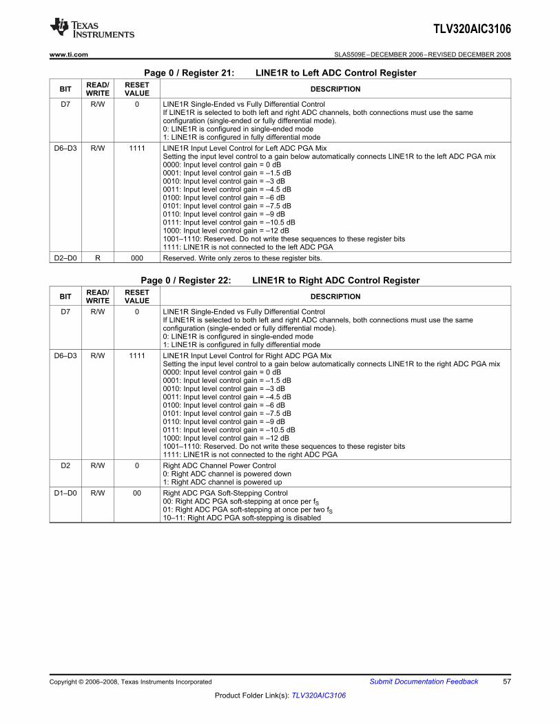
TLV320AIC3106
www.ti.com ........................................................................................................................................ SLAS509E–DECEMBER 2006–REVISED DECEMBER 2008
Page 0 / Register 21: LINE1R to Left ADC Control RegisterREAD/ RESETBIT DESCRIPTIONWRITE VALUE
D7 R/W 0 LINE1R Single-Ended vs Fully Differential ControlIf LINE1R is selected to both left and right ADC channels, both connections must use the sameconfiguration (single-ended or fully differential mode).0: LINE1R is configured in single-ended mode1: LINE1R is configured in fully differential mode
D6–D3 R/W 1111 LINE1R Input Level Control for Left ADC PGA MixSetting the input level control to a gain below automatically connects LINE1R to the left ADC PGA mix0000: Input level control gain = 0 dB0001: Input level control gain = –1.5 dB0010: Input level control gain = –3 dB0011: Input level control gain = –4.5 dB0100: Input level control gain = –6 dB0101: Input level control gain = –7.5 dB0110: Input level control gain = –9 dB0111: Input level control gain = –10.5 dB1000: Input level control gain = –12 dB1001–1110: Reserved. Do not write these sequences to these register bits1111: LINE1R is not connected to the left ADC PGA
D2–D0 R 000 Reserved. Write only zeros to these register bits.
Page 0 / Register 22: LINE1R to Right ADC Control RegisterREAD/ RESETBIT DESCRIPTIONWRITE VALUE
D7 R/W 0 LINE1R Single-Ended vs Fully Differential ControlIf LINE1R is selected to both left and right ADC channels, both connections must use the sameconfiguration (single-ended or fully differential mode).0: LINE1R is configured in single-ended mode1: LINE1R is configured in fully differential mode
D6–D3 R/W 1111 LINE1R Input Level Control for Right ADC PGA MixSetting the input level control to a gain below automatically connects LINE1R to the right ADC PGA mix0000: Input level control gain = 0 dB0001: Input level control gain = –1.5 dB0010: Input level control gain = –3 dB0011: Input level control gain = –4.5 dB0100: Input level control gain = –6 dB0101: Input level control gain = –7.5 dB0110: Input level control gain = –9 dB0111: Input level control gain = –10.5 dB1000: Input level control gain = –12 dB1001–1110: Reserved. Do not write these sequences to these register bits1111: LINE1R is not connected to the right ADC PGA
D2 R/W 0 Right ADC Channel Power Control0: Right ADC channel is powered down1: Right ADC channel is powered up
D1–D0 R/W 00 Right ADC PGA Soft-Stepping Control00: Right ADC PGA soft-stepping at once per fS01: Right ADC PGA soft-stepping at once per two fS10–11: Right ADC PGA soft-stepping is disabled
Copyright © 2006–2008, Texas Instruments Incorporated Submit Documentation Feedback 57
Product Folder Link(s): TLV320AIC3106
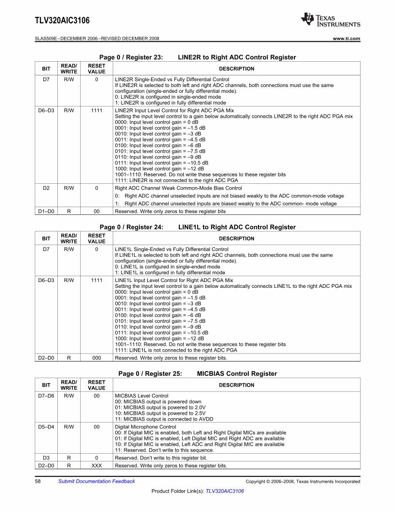
TLV320AIC3106
SLAS509E–DECEMBER 2006–REVISED DECEMBER 2008........................................................................................................................................ www.ti.com
Page 0 / Register 23: LINE2R to Right ADC Control RegisterREAD/ RESETBIT DESCRIPTIONWRITE VALUE
D7 R/W 0 LINE2R Single-Ended vs Fully Differential ControlIf LINE2R is selected to both left and right ADC channels, both connections must use the sameconfiguration (single-ended or fully differential mode).0: LINE2R is configured in single-ended mode1: LINE2R is configured in fully differential mode
D6–D3 R/W 1111 LINE2R Input Level Control for Right ADC PGA MixSetting the input level control to a gain below automatically connects LINE2R to the right ADC PGA mix0000: Input level control gain = 0 dB0001: Input level control gain = –1.5 dB0010: Input level control gain = –3 dB0011: Input level control gain = –4.5 dB0100: Input level control gain = –6 dB0101: Input level control gain = –7.5 dB0110: Input level control gain = –9 dB0111: Input level control gain = –10.5 dB1000: Input level control gain = –12 dB1001–1110: Reserved. Do not write these sequences to these register bits1111: LINE2R is not connected to the right ADC PGA
D2 R/W 0 Right ADC Channel Weak Common-Mode Bias Control0: Right ADC channel unselected inputs are not biased weakly to the ADC common-mode voltage1: Right ADC channel unselected inputs are biased weakly to the ADC common- mode voltage
D1–D0 R 00 Reserved. Write only zeros to these register bits
Page 0 / Register 24: LINE1L to Right ADC Control RegisterREAD/ RESETBIT DESCRIPTIONWRITE VALUE
D7 R/W 0 LINE1L Single-Ended vs Fully Differential ControlIf LINE1L is selected to both left and right ADC channels, both connections must use the sameconfiguration (single-ended or fully differential mode).0: LINE1L is configured in single-ended mode1: LINE1L is configured in fully differential mode
D6–D3 R/W 1111 LINE1L Input Level Control for Right ADC PGA MixSetting the input level control to a gain below automatically connects LINE1L to the right ADC PGA mix0000: Input level control gain = 0 dB0001: Input level control gain = –1.5 dB0010: Input level control gain = –3 dB0011: Input level control gain = –4.5 dB0100: Input level control gain = –6 dB0101: Input level control gain = –7.5 dB0110: Input level control gain = –9 dB0111: Input level control gain = –10.5 dB1000: Input level control gain = –12 dB1001–1110: Reserved. Do not write these sequences to these register bits1111: LINE1L is not connected to the right ADC PGA
D2–D0 R 000 Reserved. Write only zeros to these register bits.
Page 0 / Register 25: MICBIAS Control RegisterREAD/ RESETBIT DESCRIPTIONWRITE VALUE
D7–D6 R/W 00 MICBIAS Level Control00: MICBIAS output is powered down01: MICBIAS output is powered to 2.0V10: MICBIAS output is powered to 2.5V11: MICBIAS output is connected to AVDD
D5–D4 R/W 00 Digital Microphone Control00: If Digital MIC is enabled, both Left and Right Digital MICs are available01: If Digital MIC is enabled, Left Digital MIC and Right ADC are available10: If Digital MIC is enabled, Left ADC and Right Digital MIC are available11: Reserved. Don’t write to this sequence.
D3 R 0 Reserved. Don’t write to this register bit.D2–D0 R XXX Reserved. Write only zeros to these register bits.
58 Submit Documentation Feedback Copyright © 2006–2008, Texas Instruments Incorporated
Product Folder Link(s): TLV320AIC3106

TLV320AIC3106
www.ti.com ........................................................................................................................................ SLAS509E–DECEMBER 2006–REVISED DECEMBER 2008
Page 0 / Register 26: Left AGC Control Register AREAD/ RESETBIT DESCRIPTIONWRITE VALUE
D7 R/W 0 Left AGC Enable0: Left AGC is disabled1: Left AGC is enabled
D6–D4 R/W 000 Left AGC Target Level000: Left AGC target level = –5.5 dB001: Left AGC target level = –8 dB010: Left AGC target level = –10 dB011: Left AGC target level = –12 dB100: Left AGC target level = –14 dB101: Left AGC target level = –17 dB110: Left AGC target level = –20 dB111: Left AGC target level = –24 dB
D3–D2 R/W 00 Left AGC Attack TimeThese time constants(1) will not be accurate when double rate audio mode is enabled.00: Left AGC attack time = 8 ms01: Left AGC attack time = 11 ms10: Left AGC attack time = 16 ms11: Left AGC attack time = 20 ms
D1–D0 R/W 00 Left AGC Decay TimeThese time constants(1) will not be accurate when double rate audio mode is enabled.00: Left AGC decay time = 100 ms01: Left AGC decay time = 200 ms10: Left AGC decay time = 400 ms11: Left AGC decay time = 500 ms
(1) Time constants are valid when DRA is not enabled. The values would change if DRA is enabled.
Page 0 / Register 27: Left AGC Control Register BREAD/ RESETBIT DESCRIPTIONWRITE VALUE
D7–D1 R/W 1111 111 Left AGC Maximum Gain Allowed0000 000: Maximum gain = 0 dB0000 001: Maximum gain = 0.5 dB0000 010: Maximum gain = 1 dB…1110 110: Maximum gain = 59 dB1110 111–1111 111: Maximum gain = 59.5 dB
D0 R/W 0 Reserved. Write only zero to this register bit.
Page 0 / Register 28: Left AGC Control Register CREAD/ RESETBIT DESCRIPTIONWRITE VALUE
D7–D6 R/W 00 Noise Gate Hysteresis Level Control00: Hysteresis = 1 dB01: Hysteresis = 2 dB10: Hysteresis = 3 dB11: Hysteresis is disabled
D5–D1 R/W 00 000 Left AGC Noise Threshold Control00 000: Left AGC Noise/Silence Detection disabled00 001: Left AGC noise threshold = –30 dB00 010: Left AGC noise threshold = –32 dB00 011: Left AGC noise threshold = –34 dB…11 101: Left AGC noise threshold = –86 dB11 110: Left AGC noise threshold = –88 dB11 111: Left AGC noise threshold = –90 dB
D0 R/W 0 Left AGC Clip Stepping Control0: Left AGC clip stepping disabled1: Left AGC clip stepping enabled
Copyright © 2006–2008, Texas Instruments Incorporated Submit Documentation Feedback 59
Product Folder Link(s): TLV320AIC3106
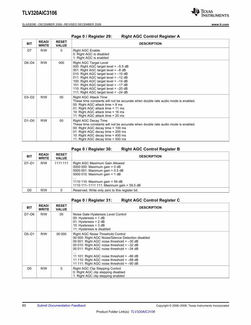
TLV320AIC3106
SLAS509E–DECEMBER 2006–REVISED DECEMBER 2008........................................................................................................................................ www.ti.com
Page 0 / Register 29: Right AGC Control Register AREAD/ RESETBIT DESCRIPTIONWRITE VALUE
D7 R/W 0 Right AGC Enable0: Right AGC is disabled1: Right AGC is enabled
D6–D4 R/W 000 Right AGC Target Level000: Right AGC target level = –5.5 dB001: Right AGC target level = –8 dB010: Right AGC target level = –10 dB011: Right AGC target level = –12 dB100: Right AGC target level = –14 dB101: Right AGC target level = –17 dB110: Right AGC target level = –20 dB111: Right AGC target level = –24 dB
D3–D2 R/W 00 Right AGC Attack TimeThese time constants will not be accurate when double rate audio mode is enabled.00: Right AGC attack time = 8 ms01: Right AGC attack time = 11 ms10: Right AGC attack time = 16 ms11: Right AGC attack time = 20 ms
D1–D0 R/W 00 Right AGC Decay TimeThese time constants will not be accurate when double rate audio mode is enabled.00: Right AGC decay time = 100 ms01: Right AGC decay time = 200 ms10: Right AGC decay time = 400 ms11: Right AGC decay time = 500 ms
Page 0 / Register 30: Right AGC Control Register BREAD/ RESETBIT DESCRIPTIONWRITE VALUE
D7–D1 R/W 1111 111 Right AGC Maximum Gain Allowed0000 000: Maximum gain = 0 dB0000 001: Maximum gain = 0.5 dB0000 010: Maximum gain = 1 dB…1110 110: Maximum gain = 59 dB1110 111–1111 111: Maximum gain = 59.5 dB
D0 R/W 0 Reserved. Write only zero to this register bit.
Page 0 / Register 31: Right AGC Control Register CREAD/ RESETBIT DESCRIPTIONWRITE VALUE
D7–D6 R/W 00 Noise Gate Hysteresis Level Control00: Hysteresis = 1 dB01: Hysteresis = 2 dB10: Hysteresis = 3 dB11: Hysteresis is disabled
D5–D1 R/W 00 000 Right AGC Noise Threshold Control00 000: Right AGC Noise/Silence Detection disabled00 001: Right AGC noise threshold = –30 dB00 010: Right AGC noise threshold = –32 dB00 011: Right AGC noise threshold = –34 dB…11 101: Right AGC noise threshold = –86 dB11 110: Right AGC noise threshold = –88 dB11 111: Right AGC noise threshold = –90 dB
D0 R/W 0 Right AGC Clip Stepping Control0: Right AGC clip stepping disabled1: Right AGC clip stepping enabled
60 Submit Documentation Feedback Copyright © 2006–2008, Texas Instruments Incorporated
Product Folder Link(s): TLV320AIC3106

TLV320AIC3106
www.ti.com ........................................................................................................................................ SLAS509E–DECEMBER 2006–REVISED DECEMBER 2008
Page 0 / Register 32: Left AGC Gain RegisterREAD/ RESETBIT DESCRIPTIONWRITE VALUE
D7–D0 R 0000 0000 Left Channel Gain Applied by AGC Algorithm1110 1000: Gain = –12 dB1110 1001: Gain = –11.5 dB1110 1010: Gain = –11 dB…0000 0000: Gain = 0 dB0000 0001: Gain = 0.5 dB…0111 0110: Gain = 59 dB0111 0111: Gain = 59.5 dB
Page 0 / Register 33: Right AGC Gain RegisterREAD/ RESETBIT DESCRIPTIONWRITE VALUE
D7–D0 R 0000 0000 Right Channel Gain Applied by AGC Algorithm1110 1000: Gain = –12 dB1110 1001: Gain = –11.5 dB1110 1010: Gain = –11 dB…0000 0000: Gain = 0 dB0000 0001: Gain = 0.5 dB…0111 0110: Gain = 59 dB0111 0111: Gain = 59.5 dB
Page 0 / Register 34: Left AGC Noise Gate Debounce RegisterREAD/ RESETBIT DESCRIPTIONWRITE VALUE
D7–D3 R/W 0000 0 Left AGC Noise Detection Debounce ControlThese times(1) will not be accurate when double rate audio mode is enabled.0000 0: Debounce = 0 ms0000 1: Debounce = 0.5 ms0001 0: Debounce = 1 ms0001 1: Debounce = 2 ms0010 0: Debounce = 4 ms0010 1: Debounce = 8 ms0011 0: Debounce = 16 ms0011 1: Debounce = 32 ms0100 0: Debounce = 64×1 = 64ms0100 1: Debounce = 64×2 = 128ms0101 0: Debounce = 64×3 = 192ms…1111 0: Debounce = 64×23 = 1472ms1111 1: Debounce = 64×24 = 1536ms
D2–D0 R/W 000 Left AGC Signal Detection Debounce ControlThese times(1) will not be accurate when double rate audio mode is enabled.000: Debounce = 0 ms001: Debounce = 0.5 ms010: Debounce = 1 ms011: Debounce = 2 ms100: Debounce = 4 ms101: Debounce = 8 ms110: Debounce = 16 ms111: Debounce = 32 ms
(1) Time constants are valid when DRA is not enabled. The values would change when DRA is enabled
Copyright © 2006–2008, Texas Instruments Incorporated Submit Documentation Feedback 61
Product Folder Link(s): TLV320AIC3106
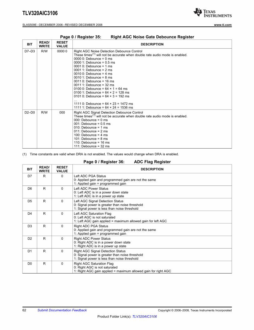
TLV320AIC3106
SLAS509E–DECEMBER 2006–REVISED DECEMBER 2008........................................................................................................................................ www.ti.com
Page 0 / Register 35: Right AGC Noise Gate Debounce RegisterREAD/ RESETBIT DESCRIPTIONWRITE VALUE
D7–D3 R/W 0000 0 Right AGC Noise Detection Debounce ControlThese times(1) will not be accurate when double rate audio mode is enabled.0000 0: Debounce = 0 ms0000 1: Debounce = 0.5 ms0001 0: Debounce = 1 ms0001 1: Debounce = 2 ms0010 0: Debounce = 4 ms0010 1: Debounce = 8 ms0011 0: Debounce = 16 ms0011 1: Debounce = 32 ms0100 0: Debounce = 64 × 1 = 64 ms0100 1: Debounce = 64 × 2 = 128 ms0101 0: Debounce = 64 × 3 = 192 ms…1111 0: Debounce = 64 × 23 = 1472 ms1111 1: Debounce = 64 × 24 = 1536 ms
D2–D0 R/W 000 Right AGC Signal Detection Debounce ControlThese times(1) will not be accurate when double rate audio mode is enabled.000: Debounce = 0 ms001: Debounce = 0.5 ms010: Debounce = 1 ms011: Debounce = 2 ms100: Debounce = 4 ms101: Debounce = 8 ms110: Debounce = 16 ms111: Debounce = 32 ms
(1) Time constants are valid when DRA is not enabled. The values would change when DRA is enabled.
Page 0 / Register 36: ADC Flag RegisterREAD/ RESETBIT DESCRIPTIONWRITE VALUE
D7 R 0 Left ADC PGA Status0: Applied gain and programmed gain are not the same1: Applied gain = programmed gain
D6 R 0 Left ADC Power Status0: Left ADC is in a power down state1: Left ADC is in a power up state
D5 R 0 Left AGC Signal Detection Status0: Signal power is greater than noise threshold1: Signal power is less than noise threshold
D4 R 0 Left AGC Saturation Flag0: Left AGC is not saturated1: Left AGC gain applied = maximum allowed gain for left AGC
D3 R 0 Right ADC PGA Status0: Applied gain and programmed gain are not the same1: Applied gain = programmed gain
D2 R 0 Right ADC Power Status0: Right ADC is in a power down state1: Right ADC is in a power up state
D1 R 0 Right AGC Signal Detection Status0: Signal power is greater than noise threshold1: Signal power is less than noise threshold
D0 R 0 Right AGC Saturation Flag0: Right AGC is not saturated1: Right AGC gain applied = maximum allowed gain for right AGC
62 Submit Documentation Feedback Copyright © 2006–2008, Texas Instruments Incorporated
Product Folder Link(s): TLV320AIC3106

TLV320AIC3106
www.ti.com ........................................................................................................................................ SLAS509E–DECEMBER 2006–REVISED DECEMBER 2008
Page 0 / Register 37: DAC Power and Output Driver Control RegisterREAD/ RESETBIT DESCRIPTIONWRITE VALUE
D7 R/W 0 Left DAC Power Control0: Left DAC not powered up1: Left DAC is powered up
D6 R/W 0 Right DAC Power Control0: Right DAC not powered up1: Right DAC is powered up
D5–D4 R/W 00 HPLCOM Output Driver Configuration Control00: HPLCOM configured as differential of HPLOUT01: HPLCOM configured as constant VCM output10: HPLCOM configured as independent single-ended output11: Reserved. Do not write this sequence to these register bits.
D3–D0 R 000 Reserved. Write only zeros to these register bits.
Page 0 / Register 38: High-Power Output Driver Control RegisterREAD/ RESETBIT DESCRIPTIONWRITE VALUE
D7–D6 R 00 Reserved. Write only zeros to these register bits.D5–D3 R/W 000 HPRCOM Output Driver Configuration Control
000: HPRCOM configured as differential of HPROUT001: HPRCOM configured as constant VCM output010: HPRCOM configured as independent single-ended output011: HPRCOM configured as differential of HPLCOM100: HPRCOM configured as external feedback with HPLCOM as constant VCM output101–111: Reserved. Do not write these sequences to these register bits.
D2 R/W 0 Short Circuit Protection Control0: Short circuit protection on all high power output drivers is disabled1: Short circuit protection on all high power output drivers is enabled
D1 R/W 0 Short-Circuit Protection Mode Control0: If short circuit protection enabled, it will limit the maximum current to the load1: If short circuit protection enabled, it will power down the output driver automatically when a shortis detected
D0 R 0 Reserved. Write only zero to this register bit.
Page 0 / Register 39: Reserved RegisterREAD/ RESETBIT DESCRIPTIONWRITE VALUE
D7–D0 R 0000 0000 Reserved. Do not write to this register.
Copyright © 2006–2008, Texas Instruments Incorporated Submit Documentation Feedback 63
Product Folder Link(s): TLV320AIC3106
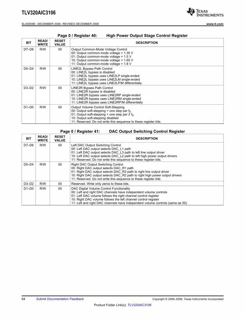
TLV320AIC3106
SLAS509E–DECEMBER 2006–REVISED DECEMBER 2008........................................................................................................................................ www.ti.com
Page 0 / Register 40: High Power Output Stage Control RegisterREAD/ RESETBIT DESCRIPTIONWRITE VALUE
D7–D6 R/W 00 Output Common-Mode Voltage Control00: Output common-mode voltage = 1.35 V01: Output common-mode voltage = 1.5 V10: Output common-mode voltage = 1.65 V11: Output common-mode voltage = 1.8 V
D5–D4 R/W 00 LINE2L Bypass Path Control00: LINE2L bypass is disabled01: LINE2L bypass uses LINE2LP single-ended10: LINE2L bypass uses LINE2LM single-ended11: LINE2L bypass uses LINE2LP/M differentially
D3–D2 R/W 00 LINE2R Bypass Path Control00: LINE2R bypass is disabled01: LINE2R bypass uses LINE2RP single-ended10: LINE2R bypass uses LINE2RM single-ended11: LINE2R bypass uses LINE2RP/M differentially
D1–D0 R/W 00 Output Volume Control Soft-Stepping00: Output soft-stepping = one step per fS01: Output soft-stepping = one step per 2 fS10: Output soft-stepping disabled11: Reserved. Do not write this sequence to these register bits.
Page 0 / Register 41: DAC Output Switching Control RegisterREAD/ RESETBIT DESCRIPTIONWRITE VALUE
D7–D6 R/W 00 Left DAC Output Switching Control00: Left DAC output selects DAC_L1 path01: Left DAC output selects DAC_L3 path to left line output driver10: Left DAC output selects DAC_L2 path to left high power output drivers11: Reserved. Do not write this sequence to these register bits.
D5–D4 R/W 00 Right DAC Output Switching Control00: Right DAC output selects DAC_R1 path01: Right DAC output selects DAC_R3 path to right line output driver10: Right DAC output selects DAC_R2 path to right high power output drivers11: Reserved. Do not write this sequence to these register bits.
D3–D2 R/W 00 Reserved. Write only zeros to these bits.D1–D0 R/W 00 DAC Digital Volume Control Functionality
00: Left and right DAC channels have independent volume controls01: Left DAC volume follows the right channel control register10: Right DAC volume follows the left channel control register11: Left and right DAC channels have independent volume controls (same as 00)
64 Submit Documentation Feedback Copyright © 2006–2008, Texas Instruments Incorporated
Product Folder Link(s): TLV320AIC3106
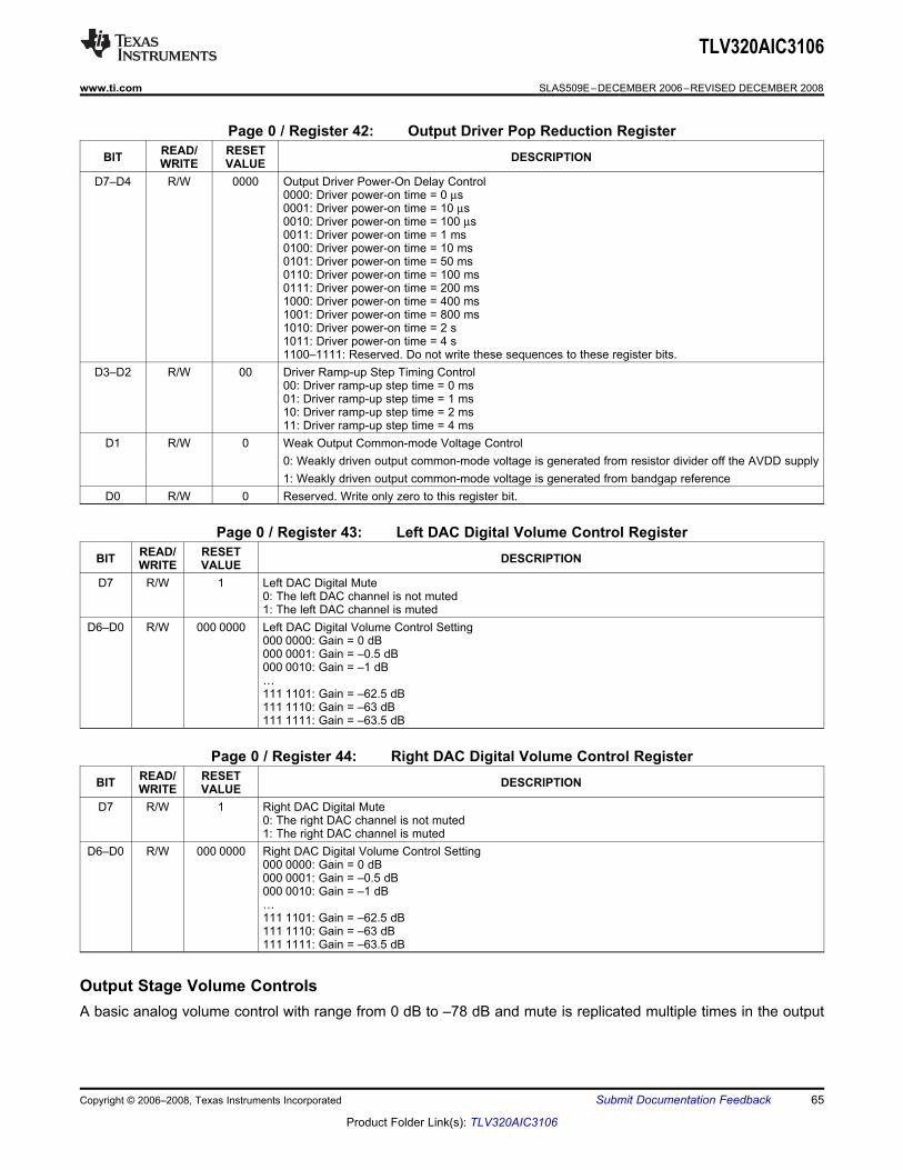
Output Stage Volume Controls
TLV320AIC3106
www.ti.com ........................................................................................................................................ SLAS509E–DECEMBER 2006–REVISED DECEMBER 2008
Page 0 / Register 42: Output Driver Pop Reduction RegisterREAD/ RESETBIT DESCRIPTIONWRITE VALUE
D7–D4 R/W 0000 Output Driver Power-On Delay Control0000: Driver power-on time = 0 µs0001: Driver power-on time = 10 µs0010: Driver power-on time = 100 µs0011: Driver power-on time = 1 ms0100: Driver power-on time = 10 ms0101: Driver power-on time = 50 ms0110: Driver power-on time = 100 ms0111: Driver power-on time = 200 ms1000: Driver power-on time = 400 ms1001: Driver power-on time = 800 ms1010: Driver power-on time = 2 s1011: Driver power-on time = 4 s1100–1111: Reserved. Do not write these sequences to these register bits.
D3–D2 R/W 00 Driver Ramp-up Step Timing Control00: Driver ramp-up step time = 0 ms01: Driver ramp-up step time = 1 ms10: Driver ramp-up step time = 2 ms11: Driver ramp-up step time = 4 ms
D1 R/W 0 Weak Output Common-mode Voltage Control0: Weakly driven output common-mode voltage is generated from resistor divider off the AVDD supply1: Weakly driven output common-mode voltage is generated from bandgap reference
D0 R/W 0 Reserved. Write only zero to this register bit.
Page 0 / Register 43: Left DAC Digital Volume Control RegisterREAD/ RESETBIT DESCRIPTIONWRITE VALUE
D7 R/W 1 Left DAC Digital Mute0: The left DAC channel is not muted1: The left DAC channel is muted
D6–D0 R/W 000 0000 Left DAC Digital Volume Control Setting000 0000: Gain = 0 dB000 0001: Gain = –0.5 dB000 0010: Gain = –1 dB…111 1101: Gain = –62.5 dB111 1110: Gain = –63 dB111 1111: Gain = –63.5 dB
Page 0 / Register 44: Right DAC Digital Volume Control RegisterREAD/ RESETBIT DESCRIPTIONWRITE VALUE
D7 R/W 1 Right DAC Digital Mute0: The right DAC channel is not muted1: The right DAC channel is muted
D6–D0 R/W 000 0000 Right DAC Digital Volume Control Setting000 0000: Gain = 0 dB000 0001: Gain = –0.5 dB000 0010: Gain = –1 dB…111 1101: Gain = –62.5 dB111 1110: Gain = –63 dB111 1111: Gain = –63.5 dB
A basic analog volume control with range from 0 dB to –78 dB and mute is replicated multiple times in the output
Copyright © 2006–2008, Texas Instruments Incorporated Submit Documentation Feedback 65
Product Folder Link(s): TLV320AIC3106
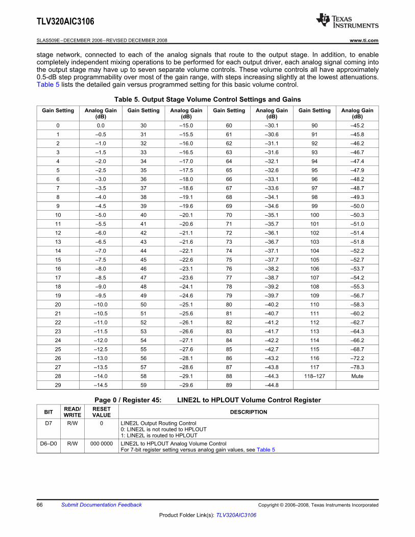
TLV320AIC3106
SLAS509E–DECEMBER 2006–REVISED DECEMBER 2008........................................................................................................................................ www.ti.com
stage network, connected to each of the analog signals that route to the output stage. In addition, to enablecompletely independent mixing operations to be performed for each output driver, each analog signal coming intothe output stage may have up to seven separate volume controls. These volume controls all have approximately0.5-dB step programmability over most of the gain range, with steps increasing slightly at the lowest attenuations.Table 5 lists the detailed gain versus programmed setting for this basic volume control.
Table 5. Output Stage Volume Control Settings and GainsGain Setting Analog Gain Gain Setting Analog Gain Gain Setting Analog Gain Gain Setting Analog Gain
(dB) (dB) (dB) (dB)0 0.0 30 –15.0 60 –30.1 90 –45.21 –0.5 31 –15.5 61 –30.6 91 –45.82 –1.0 32 –16.0 62 –31.1 92 –46.23 –1.5 33 –16.5 63 –31.6 93 –46.74 –2.0 34 –17.0 64 –32.1 94 –47.45 –2.5 35 –17.5 65 –32.6 95 –47.96 –3.0 36 –18.0 66 –33.1 96 –48.27 –3.5 37 –18.6 67 –33.6 97 –48.78 –4.0 38 –19.1 68 –34.1 98 –49.39 –4.5 39 –19.6 69 –34.6 99 –50.010 –5.0 40 –20.1 70 –35.1 100 –50.311 –5.5 41 –20.6 71 –35.7 101 –51.012 –6.0 42 –21.1 72 –36.1 102 –51.413 –6.5 43 –21.6 73 –36.7 103 –51.814 –7.0 44 –22.1 74 –37.1 104 –52.215 –7.5 45 –22.6 75 –37.7 105 –52.716 –8.0 46 –23.1 76 –38.2 106 –53.717 –8.5 47 –23.6 77 –38.7 107 –54.218 –9.0 48 –24.1 78 –39.2 108 –55.319 –9.5 49 –24.6 79 –39.7 109 –56.720 –10.0 50 –25.1 80 –40.2 110 –58.321 –10.5 51 –25.6 81 –40.7 111 –60.222 –11.0 52 –26.1 82 –41.2 112 –62.723 –11.5 53 –26.6 83 –41.7 113 –64.324 –12.0 54 –27.1 84 –42.2 114 –66.225 –12.5 55 –27.6 85 –42.7 115 –68.726 –13.0 56 –28.1 86 –43.2 116 –72.227 –13.5 57 –28.6 87 –43.8 117 –78.328 –14.0 58 –29.1 88 –44.3 118–127 Mute29 –14.5 59 –29.6 89 –44.8
Page 0 / Register 45: LINE2L to HPLOUT Volume Control RegisterREAD/ RESETBIT DESCRIPTIONWRITE VALUE
D7 R/W 0 LINE2L Output Routing Control0: LINE2L is not routed to HPLOUT1: LINE2L is routed to HPLOUT
D6–D0 R/W 000 0000 LINE2L to HPLOUT Analog Volume ControlFor 7-bit register setting versus analog gain values, see Table 5
66 Submit Documentation Feedback Copyright © 2006–2008, Texas Instruments Incorporated
Product Folder Link(s): TLV320AIC3106
TLV320AIC3106
www.ti.com ........................................................................................................................................ SLAS509E–DECEMBER 2006–REVISED DECEMBER 2008
Page 0 / Register 46: PGA_L to HPLOUT Volume Control RegisterREAD/ RESETBIT DESCRIPTIONWRITE VALUE
D7 R/W 0 PGA_L Output Routing Control0: PGA_L is not routed to HPLOUT1: PGA_L is routed to HPLOUT
D6–D0 R/W 000 0000 PGA_L to HPLOUT Analog Volume ControlFor 7-bit register setting versus analog gain values, see Table 5
Page 0 / Register 47: DAC_L1 to HPLOUT Volume Control RegisterREAD/ RESETBIT DESCRIPTIONWRITE VALUE
D7 R/W 0 DAC_L1 Output Routing Control0: DAC_L1 is not routed to HPLOUT1: DAC_L1 is routed to HPLOUT
D6–D0 R/W 000 0000 DAC_L1 to HPLOUT Analog Volume ControlFor 7-bit register setting versus analog gain values, see Table 5
Page 0 / Register 48: LINE2R to HPLOUT Volume Control RegisterREAD/ RESETBIT DESCRIPTIONWRITE VALUE
D7 R/W 0 LINE2R Output Routing Control0: LINE2R is not routed to HPLOUT1: LINE2R is routed to HPLOUT
D6–D0 R/W 000 0000 LINE2R to HPLOUT Analog Volume ControlFor 7-bit register setting versus analog gain values, see Table 5
Page 0 / Register 49: PGA_R to HPLOUT Volume Control RegisterREAD/ RESETBIT DESCRIPTIONWRITE VALUE
D7 R/W 0 PGA_R Output Routing Control0: PGA_R is not routed to HPLOUT1: PGA_R is routed to HPLOUT
D6–D0 R/W 000 0000 PGA_R to HPLOUT Analog Volume ControlFor 7-bit register setting versus analog gain values, see Table 5
Page 0 / Register 50: DAC_R1 to HPLOUT Volume Control RegisterREAD/ RESETBIT DESCRIPTIONWRITE VALUE
D7 R/W 0 DAC_R1 Output Routing Control0: DAC_R1 is not routed to HPLOUT1: DAC_R1 is routed to HPLOUT
D6–D0 R/W 000 0000 DAC_R1 to HPLOUT Analog Volume ControlFor 7-bit register setting versus analog gain values, see Table 5
Copyright © 2006–2008, Texas Instruments Incorporated Submit Documentation Feedback 67
Product Folder Link(s): TLV320AIC3106

TLV320AIC3106
SLAS509E–DECEMBER 2006–REVISED DECEMBER 2008........................................................................................................................................ www.ti.com
Page 0 / Register 51: HPLOUT Output Level Control RegisterREAD/ RESETBIT DESCRIPTIONWRITE VALUE
D7–D4 R/W 0000 HPLOUT Output Level Control0000: Output level control = 0-dB0001: Output level control = 1-dB0010: Output level control = 2-dB...1000: Output level control = 8-dB1001: Output level control = 9-dB1010–1111: Reserved. Do not write these sequences to these register bits.
D3 R/W 0 HPLOUT Mute0: HPLOUT is muted1: HPLOUT is not muted
D2 R/W 1 HPLOUT Power Down Drive Control0: HPLOUT is weakly driven to a common-mode when powered down1: HPLOUT is high-impedance when powered down
D1 R 1 HPLOUT Volume Control Status0: All programmed gains to HPLOUT have been applied1: Not all programmed gains to HPLOUT have been applied yet
D0 R/W 0 HPLOUT Power Control0: HPLOUT is not fully powered up1: HPLOUT is fully powered up
Page 0 / Register 52: LINE2L to HPLCOM Volume Control RegisterREAD/ RESETBIT DESCRIPTIONWRITE VALUE
D7 R/W 0 LINE2L Output Routing Control0: LINE2L is not routed to HPLCOM1: LINE2L is routed to HPLCOM
D6–D0 R/W 000 0000 LINE2L to HPLCOM Analog Volume ControlFor 7-bit register setting versus analog gain values, see Table 5
Page 0 / Register 53: PGA_L to HPLCOM Volume Control RegisterREAD/ RESETBIT DESCRIPTIONWRITE VALUE
D7 R/W 0 PGA_L Output Routing Control0: PGA_L is not routed to HPLCOM1: PGA_L is routed to HPLCOM
D6–D0 R/W 000 0000 PGA_L to HPLCOM Analog Volume ControlFor 7-bit register setting versus analog gain values, see Table 5
Page 0 / Register 54: DAC_L1 to HPLCOM Volume Control RegisterREAD/ RESETBIT DESCRIPTIONWRITE VALUE
D7 R/W 0 DAC_L1 Output Routing Control0: DAC_L1 is not routed to HPLCOM1: DAC_L1 is routed to HPLCOM
D6–D0 R/W 000 0000 DAC_L1 to HPLCOM Analog Volume ControlFor 7-bit register setting versus analog gain values, see Table 5
Page 0 / Register 55: LINE2R to HPLCOM Volume Control RegisterREAD/ RESETBIT DESCRIPTIONWRITE VALUE
D7 R/W 0 LINE2R Output Routing Control0: LINE2R is not routed to HPLCOM1: LINE2R is routed to HPLCOM
D6–D0 R/W 000 0000 LINE2R to HPLCOM Analog Volume ControlFor 7-bit register setting versus analog gain values, see Table 5
68 Submit Documentation Feedback Copyright © 2006–2008, Texas Instruments Incorporated
Product Folder Link(s): TLV320AIC3106

TLV320AIC3106
www.ti.com ........................................................................................................................................ SLAS509E–DECEMBER 2006–REVISED DECEMBER 2008
Page 0 / Register 56: PGA_R to HPLCOM Volume Control RegisterREAD/ RESETBIT DESCRIPTIONWRITE VALUE
D7 R/W 0 PGA_R Output Routing Control0: PGA_R is not routed to HPLCOM1: PGA_R is routed to HPLCOM
D6–D0 R/W 000 0000 PGA_R to HPLCOM Analog Volume ControlFor 7-bit register setting versus analog gain values, see Table 5
Page 0 / Register 57: DAC_R1 to HPLCOM Volume Control RegisterREAD/ RESETBIT DESCRIPTIONWRITE VALUE
D7 R/W 0 DAC_R1 Output Routing Control0: DAC_R1 is not routed to HPLCOM1: DAC_R1 is routed to HPLCOM
D6–D0 R/W 000 0000 DAC_R1 to HPLCOM Analog Volume ControlFor 7-bit register setting versus analog gain values, see Table 5
Page 0 / Register 58: HPLCOM Output Level Control RegisterREAD/ RESETBIT DESCRIPTIONWRITE VALUE
D7–D4 R/W 0000 HPLCOM Output Level Control0000: Output level control = 0 dB0001: Output level control = 1 dB0010: Output level control = 2 dB...1000: Output level control = 8 dB1001: Output level control = 9 dB1010–1111: Reserved. Do not write these sequences to these register bits.
D3 R/W 0 HPLCOM Mute0: HPLCOM is muted1: HPLCOM is not muted
D2 R/W 1 HPLCOM Power Down Drive Control0: HPLCOM is weakly driven to a common-mode when powered down1: HPLCOM is high-impedance when powered down.
D1 R 1 HPLCOM Volume Control Status0: All programmed gains to HPLCOM have been applied1: Not all programmed gains to HPLCOM have been applied yet
D0 R/W 0 HPLCOM Power Control0: HPLCOM is not fully powered up1: HPLCOM is fully powered up
Page 0 / Register 59: LINE2L to HPROUT Volume Control RegisterREAD/ RESETBIT DESCRIPTIONWRITE VALUE
D7 R/W 0 LINE2L Output Routing Control0: LINE2L is not routed to HPROUT1: LINE2L is routed to HPROUT
D6–D0 R/W 000 0000 LINE2L to HPROUT Analog Volume ControlFor 7-bit register setting versus analog gain values, see Table 5
Page 0 / Register 60: PGA_L to HPROUT Volume Control RegisterREAD/ RESETBIT DESCRIPTIONWRITE VALUE
D7 R/W 0 PGA_L Output Routing Control0: PGA_L is not routed to HPROUT1: PGA_L is routed to HPROUT
D6–D0 R/W 000 0000 PGA_L to HPROUT Analog Volume ControlFor 7-bit register setting versus analog gain values, see Table 5
Copyright © 2006–2008, Texas Instruments Incorporated Submit Documentation Feedback 69
Product Folder Link(s): TLV320AIC3106
TLV320AIC3106
SLAS509E–DECEMBER 2006–REVISED DECEMBER 2008........................................................................................................................................ www.ti.com
Page 0 / Register 61: DAC_L1 to HPROUT Volume Control RegisterREAD/ RESETBIT DESCRIPTIONWRITE VALUE
D7 R/W 0 DAC_L1 Output Routing Control0: DAC_L1 is not routed to HPROUT1: DAC_L1 is routed to HPROUT
D6–D0 R/W 000 0000 DAC_L1 to HPROUT Analog Volume ControlFor 7-bit register setting versus analog gain values, see Table 5
Page 0 / Register 62: LINE2R to HPROUT Volume Control RegisterREAD/ RESETBIT DESCRIPTIONWRITE VALUE
D7 R/W 0 LINE2R Output Routing Control0: LINE2R is not routed to HPROUT1: LINE2R is routed to HPROUT
D6–D0 R/W 000 0000 LINE2R to HPROUT Analog Volume ControlFor 7-bit register setting versus analog gain values, see Table 5
Page 0 / Register 63: PGA_R to HPROUT Volume Control RegisterREAD/ RESETBIT DESCRIPTIONWRITE VALUE
D7 R/W 0 PGA_R Output Routing Control0: PGA_R is not routed to HPROUT1: PGA_R is routed to HPROUT
D6–D0 R/W 000 0000 PGA_R to HPROUT Analog Volume ControlFor 7-bit register setting versus analog gain values, see Table 5
Page 0 / Register 64: DAC_R1 to HPROUT Volume Control RegisterREAD/ RESETBIT DESCRIPTIONWRITE VALUE
D7 R/W 0 DAC_R1 Output Routing Control0: DAC_R1 is not routed to HPROUT1: DAC_R1 is routed to HPROUT
D6–D0 R/W 000 0000 DAC_R1 to HPROUT Analog Volume ControlFor 7-bit register setting versus analog gain values, see Table 5
Page 0 / Register 65: HPROUT Output Level Control RegisterREAD/ RESETBIT DESCRIPTIONWRITE VALUE
D7–D4 R/W 0000 HPROUT Output Level Control0000: Output level control = 0 dB0001: Output level control = 1 dB0010: Output level control = 2 dB...1000: Output level control = 8 dB1001: Output level control = 9 dB1010–1111: Reserved. Do not write these sequences to these register bits.
D3 R/W 0 HPROUT Mute0: HPROUT is muted1: HPROUT is not muted
D2 R/W 1 HPROUT Power Down Drive Control0: HPROUT is weakly driven to a common-mode when powered down1: HPROUT is high-impedance when powered down
D1 R 1 HPROUT Volume Control Status0: All programmed gains to HPROUT have been applied1: Not all programmed gains to HPROUT have been applied yet
D0 R/W 0 HPROUT Power Control0: HPROUT is not fully powered up1: HPROUT is fully powered up
70 Submit Documentation Feedback Copyright © 2006–2008, Texas Instruments Incorporated
Product Folder Link(s): TLV320AIC3106
TLV320AIC3106
www.ti.com ........................................................................................................................................ SLAS509E–DECEMBER 2006–REVISED DECEMBER 2008
Page 0 / Register 66: LINE2L to HPRCOM Volume Control RegisterREAD/ RESETBIT DESCRIPTIONWRITE VALUE
D7 R/W 0 LINE2L Output Routing Control0: LINE2L is not routed to HPRCOM1: LINE2L is routed to HPRCOM
D6–D0 R/W 000 0000 LINE2L to HPRCOM Analog Volume ControlFor 7-bit register setting versus analog gain values, see Table 5
Page 0 / Register 67: PGA_L to HPRCOM Volume Control RegisterREAD/ RESETBIT DESCRIPTIONWRITE VALUE
D7 R/W 0 PGA_L Output Routing Control0: PGA_L is not routed to HPRCOM1: PGA_L is routed to HPRCOM
D6–D0 R/W 000 0000 PGA_L to HPRCOM Analog Volume ControlFor 7-bit register setting versus analog gain values, see Table 5
Page 0 / Register 68: DAC_L1 to HPRCOM Volume Control RegisterREAD/ RESETBIT DESCRIPTIONWRITE VALUE
D7 R/W 0 DAC_L1 Output Routing Control0: DAC_L1 is not routed to HPRCOM1: DAC_L1 is routed to HPRCOM
D6–D0 R/W 000 0000 DAC_L1 to HPRCOM Analog Volume ControlFor 7-bit register setting versus analog gain values, see Table 5
Page 0 / Register 69: LINE2R to HPRCOM Volume Control RegisterREAD/ RESETBIT DESCRIPTIONWRITE VALUE
D7 R/W 0 LINE2R Output Routing Control0: LINE2R is not routed to HPRCOM1: LINE2R is routed to HPRCOM
D6–D0 R/W 000 0000 LINE2R to HPRCOM Analog Volume ControlFor 7-bit register setting versus analog gain values, see Table 5
Page 0 / Register 70: PGA_R to HPRCOM Volume Control RegisterREAD/ RESETBIT DESCRIPTIONWRITE VALUE
D7 R/W 0 PGA_R Output Routing Control0: PGA_R is not routed to HPRCOM1: PGA_R is routed to HPRCOM
D6–D0 R/W 000 0000 PGA_R to HPRCOM Analog Volume ControlFor 7-bit register setting versus analog gain values, see Table 5
Page 0 / Register 71: DAC_R1 to HPRCOM Volume Control RegisterREAD/ RESETBIT DESCRIPTIONWRITE VALUE
D7 R/W 0 DAC_R1 Output Routing Control0: DAC_R1 is not routed to HPRCOM1: DAC_R1 is routed to HPRCOM
D6–D0 R/W 000 0000 DAC_R1 to HPRCOM Analog Volume ControlFor 7-bit register setting versus analog gain values, see Table 5
Copyright © 2006–2008, Texas Instruments Incorporated Submit Documentation Feedback 71
Product Folder Link(s): TLV320AIC3106
TLV320AIC3106
SLAS509E–DECEMBER 2006–REVISED DECEMBER 2008........................................................................................................................................ www.ti.com
Page 0 / Register 72: HPRCOM Output Level Control RegisterREAD/ RESETBIT DESCRIPTIONWRITE VALUE
D7–D4 R/W 0000 HPRCOM Output Level Control0000: Output level control = 0 dB0001: Output level control = 1 dB0010: Output level control = 2 dB...1000: Output level control = 8 dB1001: Output level control = 9 dB1010–1111: Reserved. Do not write these sequences to these register bits.
D3 R/W 0 HPRCOM Mute0: HPRCOM is muted1: HPRCOM is not muted
D2 R/W 1 HPRCOM Power Down Drive Control0: HPRCOM is weakly driven to a common-mode when powered down1: HPRCOM is high-impedance when powered down
D1 R 1 HPRCOM Volume Control Status0: All programmed gains to HPRCOM have been applied1: Not all programmed gains to HPRCOM have been applied yet
D0 R/W 0 HPRCOM Power Control0: HPRCOM is not fully powered up1: HPRCOM is fully powered up
Page 0 / Register 73: LINE2L to MONO_LOP/M Volume Control RegisterREAD/ RESETBIT DESCRIPTIONWRITE VALUE
D7 R/W 0 LINE2L Output Routing Control0: LINE2L is not routed to MONO_LOP/M1: LINE2L is routed to MONO_LOP/M
D6–D0 R/W 000 0000 LINE2L to MONO_LOP/M Analog Volume ControlFor 7-bit register setting versus analog gain values, see Table 5
Page 0 / Register 74: PGA_L to MONO_LOP/M Volume Control RegisterREAD/ RESETBIT DESCRIPTIONWRITE VALUE
D7 R/W 0 PGA_L Output Routing Control0: PGA_L is not routed to MONO_LOP/M1: PGA_L is routed to MONO_LOP/M
D6–D0 R/W 000 0000 PGA_L to MONO_LOP/M Analog Volume ControlFor 7-bit register setting versus analog gain values, see Table 5
Page 0 / Register 75: DAC_L1 to MONO_LOP/M Volume Control RegisterREAD/ RESETBIT DESCRIPTIONWRITE VALUE
D7 R/W 0 DAC_L1 Output Routing Control0: DAC_L1 is not routed to MONO_LOP/M1: DAC_L1 is routed to MONO_LOP/M
D6–D0 R/W 000 0000 DAC_L1 to MONO_LOP/M Analog Volume ControlFor 7-bit register setting versus analog gain values, see Table 5
Page 0 / Register 76: LINE2R to MONO_LOP/M Volume Control RegisterREAD/ RESETBIT DESCRIPTIONWRITE VALUE
D7 R/W 0 LINE2R Output Routing Control0: LINE2R is not routed to MONO_LOP/M1: LINE2R is routed to MONO_LOP/M
D6–D0 R/W 000 0000 LINE2R to MONO_LOP/M Analog Volume ControlFor 7-bit register setting versus analog gain values, see Table 5
72 Submit Documentation Feedback Copyright © 2006–2008, Texas Instruments Incorporated
Product Folder Link(s): TLV320AIC3106

TLV320AIC3106
www.ti.com ........................................................................................................................................ SLAS509E–DECEMBER 2006–REVISED DECEMBER 2008
Page 0 / Register 77: PGA_R to MONO_LOP/M Volume Control RegisterREAD/ RESETBIT DESCRIPTIONWRITE VALUE
D7 R/W 0 PGA_R Output Routing Control0: PGA_R is not routed to MONO_LOP/M1: PGA_R is routed to MONO_LOP/M
D6–D0 R/W 000 0000 PGA_R to MONO_LOP/M Analog Volume ControlFor 7-bit register setting versus analog gain values, see Table 5
Page 0 / Register 78: DAC_R1 to MONO_LOP/M Volume Control RegisterREAD/ RESETBIT DESCRIPTIONWRITE VALUE
D7 R/W 0 DAC_R1 Output Routing Control0: DAC_R1 is not routed to MONO_LOP/M1: DAC_R1 is routed to MONO_LOP/M
D6–D0 R/W 000 0000 DAC_R1 to MONO_LOP/M Analog Volume ControlFor 7-bit register setting versus analog gain values, see Table 5
Page 0 / Register 79: MONO_LOP/M Output Level Control RegisterREAD/ RESETBIT DESCRIPTIONWRITE VALUE
D7–D4 R/W 0000 MONO_LOP/M Output Level Control0000: Output level control = 0 dB0001: Output level control = 1 dB0010: Output level control = 2 dB...1000: Output level control = 8 dB1001: Output level control = 9 dB1010–1111: Reserved. Do not write these sequences to these register bits.
D3 R/W 0 MONO_LOP/M Mute0: MONO_LOP/M is muted1: MONO_LOP/M is not muted
D2 R 0 Reserved. Don’t write to this register bit.D1 R 1 MONO_LOP/M Volume Control Status
0: All programmed gains to MONO_LOP/M have been applied1: Not all programmed gains to MONO_LOP/M have been applied yet
D0 R 0 MONO_LOP/M Power Status0: MONO_LOP/M is not fully powered up1: MONO_LOP/M is fully powered up
Page 0 / Register 80: LINE2L to LEFT_LOP/M Volume Control RegisterREAD/ RESETBIT DESCRIPTIONWRITE VALUE
D7 R/W 0 LINE2L Output Routing Control0: LINE2L is not routed to LEFT_LOP/M1: LINE2L is routed to LEFT_LOP/M
D6–D0 R/W 000 0000 LINE2L to LEFT_LOP/M Analog Volume ControlFor 7-bit register setting versus analog gain values, see Table 5
Page 0 / Register 81: PGA_L to LEFT_LOP/M Volume Control RegisterREAD/ RESETBIT DESCRIPTIONWRITE VALUE
D7 R/W 0 PGA_L Output Routing Control0: PGA_L is not routed to LEFT_LOP/M1: PGA_L is routed to LEFT_LOP/M
D6–D0 R/W 000 0000 PGA_L to LEFT_LOP/M Analog Volume ControlFor 7-bit register setting versus analog gain values, see Table 5
Copyright © 2006–2008, Texas Instruments Incorporated Submit Documentation Feedback 73
Product Folder Link(s): TLV320AIC3106

TLV320AIC3106
SLAS509E–DECEMBER 2006–REVISED DECEMBER 2008........................................................................................................................................ www.ti.com
Page 0 / Register 82: DAC_L1 to LEFT_LOP/M Volume Control RegisterREAD/ RESETBIT DESCRIPTIONWRITE VALUE
D7 R/W 0 DAC_L1 Output Routing Control0: DAC_L1 is not routed to LEFT_LOP/M1: DAC_L1 is routed to LEFT_LOP/M
D6–D0 R/W 000 0000 DAC_L1 to LEFT_LOP/M Analog Volume ControlFor 7-bit register setting versus analog gain values, see Table 5
Page 0 / Register 83: LINE2R to LEFT_LOP/M Volume Control RegisterREAD/ RESETBIT DESCRIPTIONWRITE VALUE
D7 R/W 0 LINE2R Output Routing Control0: LINE2R is not routed to LEFT_LOP/M1: LINE2R is routed to LEFT_LOP/M
D6–D0 R/W 000 0000 LINE2R to LEFT_LOP/M Analog Volume ControlFor 7-bit register setting versus analog gain values, see Table 5
Page 0 / Register 84: PGA_R to LEFT_LOP/M Volume Control RegisterREAD/ RESETBIT DESCRIPTIONWRITE VALUE
D7 R/W 0 PGA_R Output Routing Control0: PGA_R is not routed to LEFT_LOP/M1: PGA_R is routed to LEFT_LOP/M
D6–D0 R/W 000 0000 PGA_R to LEFT_LOP/M Analog Volume ControlFor 7-bit register setting versus analog gain values, see Table 5
Page 0 / Register 85: DAC_R1 to LEFT_LOP/M Volume Control RegisterREAD/ RESETBIT DESCRIPTIONWRITE VALUE
D7 R/W 0 DAC_R1 Output Routing Control0: DAC_R1 is not routed to LEFT_LOP/M1: DAC_R1 is routed to LEFT_LOP/M
D6–D0 R/W 000 0000 DAC_R1 to LEFT_LOP/M Analog Volume ControlFor 7-bit register setting versus analog gain values, see Table 5
Page 0 / Register 86: LEFT_LOP/M Output Level Control RegisterREAD/ RESETBIT DESCRIPTIONWRITE VALUE
D7–D4 R/W 0000 LEFT_LOP/M Output Level Control0000: Output level control = 0 dB0001: Output level control = 1 dB0010: Output level control = 2 dB...1000: Output level control = 8 dB1001: Output level control = 9 dB1010–1111: Reserved. Do not write these sequences to these register bits.
D3 R/W 0 LEFT_LOP/M Mute0: LEFT_LOP/M is muted1: LEFT_LOP/M is not muted
D2 R 0 Reserved. Don’t write to this register bit.D1 R 1 LEFT_LOP/M Volume Control Status
0: All programmed gains to LEFT_LOP/M have been applied1: Not all programmed gains to LEFT_LOP/M have been applied yet
D0 R 0 LEFT_LOP/M Power Status0: LEFT_LOP/M is not fully powered up1: LEFT_LOP/M is fully powered up
74 Submit Documentation Feedback Copyright © 2006–2008, Texas Instruments Incorporated
Product Folder Link(s): TLV320AIC3106

TLV320AIC3106
www.ti.com ........................................................................................................................................ SLAS509E–DECEMBER 2006–REVISED DECEMBER 2008
Page 0 / Register 87: LINE2L to RIGHT_LOP/M Volume Control RegisterREAD/ RESETBIT DESCRIPTIONWRITE VALUE
D7 R/W 0 LINE2L Output Routing Control0: LINE2L is not routed to RIGHT_LOP/M1: LINE2L is routed to RIGHT_LOP/M
D6–D0 R/W 000 0000 LINE2L to RIGHT_LOP/M Analog Volume ControlFor 7-bit register setting versus analog gain values, see Table 5
Page 0 / Register 88: PGA_L to RIGHT_LOP/M Volume Control RegisterREAD/ RESETBIT DESCRIPTIONWRITE VALUE
D7 R/W 0 PGA_L Output Routing Control0: PGA_L is not routed to RIGHT_LOP/M1: PGA_L is routed to RIGHT_LOP/M
D6–D0 R/W 000 0000 PGA_L to RIGHT_LOP/M Analog Volume ControlFor 7-bit register setting versus analog gain values, see Table 5
Page 0 / Register 89: DAC_L1 to RIGHT_LOP/M Volume Control RegisterREAD/ RESETBIT DESCRIPTIONWRITE VALUE
D7 R/W 0 DAC_L1 Output Routing Control0: DAC_L1 is not routed to RIGHT_LOP/M1: DAC_L1 is routed to RIGHT_LOP/M
D6–D0 R/W 000 0000 DAC_L1 to RIGHT_LOP/M Analog Volume ControlFor 7-bit register setting versus analog gain values, see Table 5
Page 0 / Register 90: LINE2R to RIGHT_LOP/M Volume Control RegisterREAD/ RESETBIT DESCRIPTIONWRITE VALUE
D7 R/W 0 LINE2R Output Routing Control0: LINE2R is not routed to RIGHT_LOP/M1: LINE2R is routed to RIGHT_LOP/M
D6–D0 R/W 000 0000 LINE2R to RIGHT_LOP/M Analog Volume ControlFor 7-bit register setting versus analog gain values, see Table 5
Page 0 / Register 91: PGA_R to RIGHT_LOP/M Volume Control RegisterREAD/ RESETBIT DESCRIPTIONWRITE VALUE
D7 R/W 0 PGA_R Output Routing Control0: PGA_R is not routed to RIGHT_LOP/M1: PGA_R is routed to RIGHT_LOP/M
D6–D0 R/W 000 0000 PGA_R to RIGHT_LOP/M Analog Volume ControlFor 7-bit register setting versus analog gain values, see Table 5
Page 0 / Register 92: DAC_R1 to RIGHT_LOP/M Volume Control RegisterREAD/ RESETBIT DESCRIPTIONWRITE VALUE
D7 R/W 0 DAC_R1 Output Routing Control0: DAC_R1 is not routed to RIGHT_LOP/M1: DAC_R1 is routed to RIGHT_LOP/M
D6–D0 R/W 000 0000 DAC_R1 to RIGHT_LOP/M Analog Volume ControlFor 7-bit register setting versus analog gain values, see Table 5
Copyright © 2006–2008, Texas Instruments Incorporated Submit Documentation Feedback 75
Product Folder Link(s): TLV320AIC3106
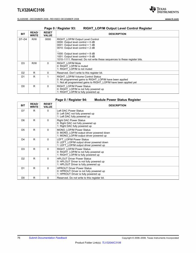
TLV320AIC3106
SLAS509E–DECEMBER 2006–REVISED DECEMBER 2008........................................................................................................................................ www.ti.com
Page 0 / Register 93: RIGHT_LOP/M Output Level Control RegisterREAD/ RESETBIT DESCRIPTIONWRITE VALUE
D7–D4 R/W 0000 RIGHT_LOP/M Output Level Control0000: Output level control = 0 dB0001: Output level control = 1 dB0010: Output level control = 2 dB...1000: Output level control = 8 dB1001: Output level control = 9 dB1010–1111: Reserved. Do not write these sequences to these register bits.
D3 R/W 0 RIGHT_LOP/M Mute0: RIGHT_LOP/M is muted1: RIGHT_LOP/M is not muted
D2 R 0 Reserved. Don’t write to this register bit.D1 R 1 RIGHT_LOP/M Volume Control Status
0: All programmed gains to RIGHT_LOP/M have been applied1: Not all programmed gains to RIGHT_LOP/M have been applied yet
D0 R 0 RIGHT_LOP/M Power Status0: RIGHT_LOP/M is not fully powered up1: RIGHT_LOP/M is fully powered up
Page 0 / Register 94: Module Power Status RegisterREAD/ RESETBIT DESCRIPTIONWRITE VALUE
D7 R 0 Left DAC Power Status0: Left DAC not fully powered up1: Left DAC fully powered up
D6 R 0 Right DAC Power Status0: Right DAC not fully powered up1: Right DAC fully powered up
D5 R 0 MONO_LOP/M Power Status0: MONO_LOP/M output driver powered down1: MONO_LOP/M output driver powered up
D4 R 0 LEFT_LOP/M Power Status0: LEFT_LOP/M output driver powered down1: LEFT_LOP/M output driver powered up
D3 R 0 RIGHT_LOP/M Power Status0: RIGHT_LOP/M is not fully powered up1: RIGHT_LOP/M is fully powered up
D2 R 0 HPLOUT Driver Power Status0: HPLOUT Driver is not fully powered up1: HPLOUT Driver is fully powered up
D1 R 0 HPROUT Driver Power Status0: HPROUT Driver is not fully powered up1: HPROUT Driver is fully powered up
D0 R 0 Reserved. Do not write to this register bit.
76 Submit Documentation Feedback Copyright © 2006–2008, Texas Instruments Incorporated
Product Folder Link(s): TLV320AIC3106
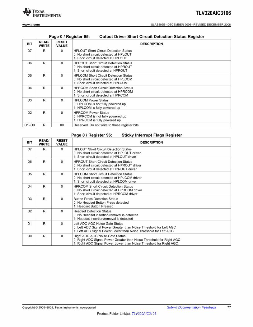
TLV320AIC3106
www.ti.com ........................................................................................................................................ SLAS509E–DECEMBER 2006–REVISED DECEMBER 2008
Page 0 / Register 95: Output Driver Short Circuit Detection Status RegisterREAD/ RESETBIT DESCRIPTIONWRITE VALUE
D7 R 0 HPLOUT Short Circuit Detection Status0: No short circuit detected at HPLOUT1: Short circuit detected at HPLOUT
D6 R 0 HPROUT Short Circuit Detection Status0: No short circuit detected at HPROUT1: Short circuit detected at HPROUT
D5 R 0 HPLCOM Short Circuit Detection Status0: No short circuit detected at HPLCOM1: Short circuit detected at HPLCOM
D4 R 0 HPRCOM Short Circuit Detection Status0: No short circuit detected at HPRCOM1: Short circuit detected at HPRCOM
D3 R 0 HPLCOM Power Status0: HPLCOM is not fully powered up1: HPLCOM is fully powered up
D2 R 0 HPRCOM Power Status0: HPRCOM is not fully powered up1: HPRCOM is fully powered up
D1–D0 R 00 Reserved. Do not write to these register bits.
Page 0 / Register 96: Sticky Interrupt Flags RegisterREAD/ RESETBIT DESCRIPTIONWRITE VALUE
D7 R 0 HPLOUT Short Circuit Detection Status0: No short circuit detected at HPLOUT driver1: Short circuit detected at HPLOUT driver
D6 R 0 HPROUT Short Circuit Detection Status0: No short circuit detected at HPROUT driver1: Short circuit detected at HPROUT driver
D5 R 0 HPLCOM Short Circuit Detection Status0: No short circuit detected at HPLCOM driver1: Short circuit detected at HPLCOM driver
D4 R 0 HPRCOM Short Circuit Detection Status0: No short circuit detected at HPRCOM driver1: Short circuit detected at HPRCOM driver
D3 R 0 Button Press Detection Status0: No Headset Button Press detected1: Headset Button Pressed
D2 R 0 Headset Detection Status0: No Headset insertion/removal is detected1: Headset insertion/removal is detected
D1 R 0 Left ADC AGC Noise Gate Status0: Left ADC Signal Power Greater than Noise Threshold for Left AGC1: Left ADC Signal Power Lower than Noise Threshold for Left AGC
D0 R 0 Right ADC AGC Noise Gate Status0: Right ADC Signal Power Greater than Noise Threshold for Right AGC1: Right ADC Signal Power Lower than Noise Threshold for Right AGC
Copyright © 2006–2008, Texas Instruments Incorporated Submit Documentation Feedback 77
Product Folder Link(s): TLV320AIC3106
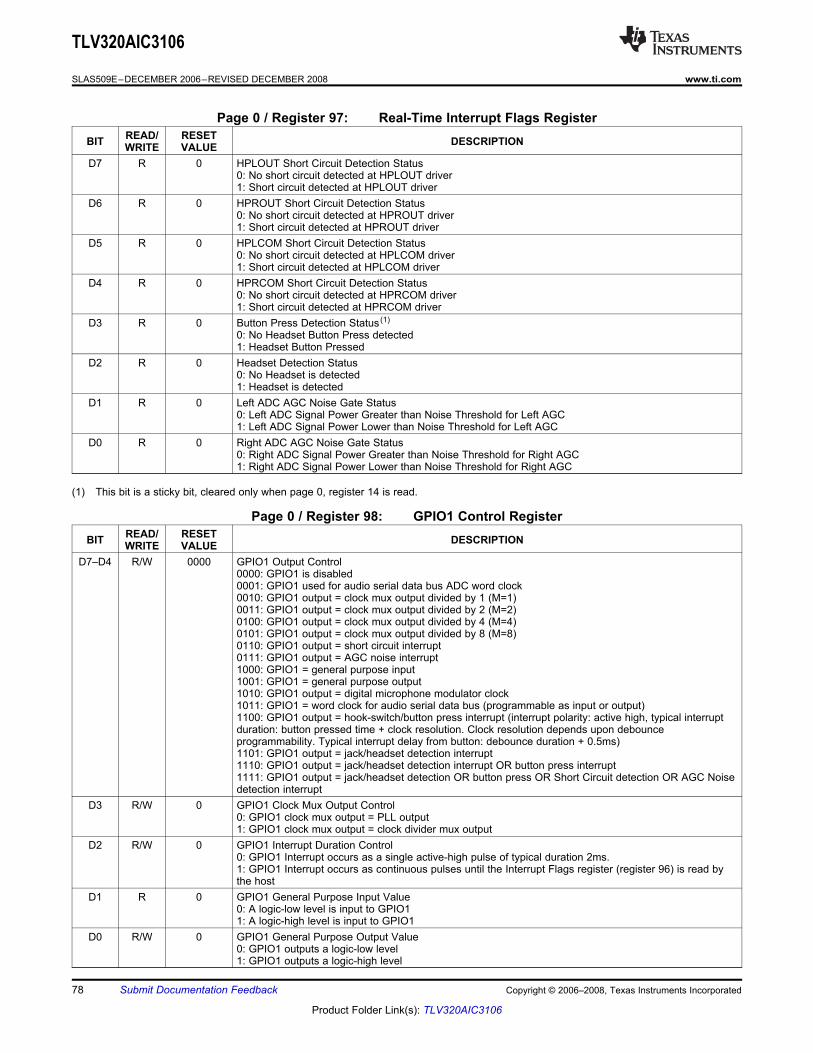
TLV320AIC3106
SLAS509E–DECEMBER 2006–REVISED DECEMBER 2008........................................................................................................................................ www.ti.com
Page 0 / Register 97: Real-Time Interrupt Flags RegisterREAD/ RESETBIT DESCRIPTIONWRITE VALUE
D7 R 0 HPLOUT Short Circuit Detection Status0: No short circuit detected at HPLOUT driver1: Short circuit detected at HPLOUT driver
D6 R 0 HPROUT Short Circuit Detection Status0: No short circuit detected at HPROUT driver1: Short circuit detected at HPROUT driver
D5 R 0 HPLCOM Short Circuit Detection Status0: No short circuit detected at HPLCOM driver1: Short circuit detected at HPLCOM driver
D4 R 0 HPRCOM Short Circuit Detection Status0: No short circuit detected at HPRCOM driver1: Short circuit detected at HPRCOM driver
D3 R 0 Button Press Detection Status(1)0: No Headset Button Press detected1: Headset Button Pressed
D2 R 0 Headset Detection Status0: No Headset is detected1: Headset is detected
D1 R 0 Left ADC AGC Noise Gate Status0: Left ADC Signal Power Greater than Noise Threshold for Left AGC1: Left ADC Signal Power Lower than Noise Threshold for Left AGC
D0 R 0 Right ADC AGC Noise Gate Status0: Right ADC Signal Power Greater than Noise Threshold for Right AGC1: Right ADC Signal Power Lower than Noise Threshold for Right AGC
(1) This bit is a sticky bit, cleared only when page 0, register 14 is read.
Page 0 / Register 98: GPIO1 Control RegisterREAD/ RESETBIT DESCRIPTIONWRITE VALUE
D7–D4 R/W 0000 GPIO1 Output Control0000: GPIO1 is disabled0001: GPIO1 used for audio serial data bus ADC word clock0010: GPIO1 output = clock mux output divided by 1 (M=1)0011: GPIO1 output = clock mux output divided by 2 (M=2)0100: GPIO1 output = clock mux output divided by 4 (M=4)0101: GPIO1 output = clock mux output divided by 8 (M=8)0110: GPIO1 output = short circuit interrupt0111: GPIO1 output = AGC noise interrupt1000: GPIO1 = general purpose input1001: GPIO1 = general purpose output1010: GPIO1 output = digital microphone modulator clock1011: GPIO1 = word clock for audio serial data bus (programmable as input or output)1100: GPIO1 output = hook-switch/button press interrupt (interrupt polarity: active high, typical interruptduration: button pressed time + clock resolution. Clock resolution depends upon debounceprogrammability. Typical interrupt delay from button: debounce duration + 0.5ms)1101: GPIO1 output = jack/headset detection interrupt1110: GPIO1 output = jack/headset detection interrupt OR button press interrupt1111: GPIO1 output = jack/headset detection OR button press OR Short Circuit detection OR AGC Noisedetection interrupt
D3 R/W 0 GPIO1 Clock Mux Output Control0: GPIO1 clock mux output = PLL output1: GPIO1 clock mux output = clock divider mux output
D2 R/W 0 GPIO1 Interrupt Duration Control0: GPIO1 Interrupt occurs as a single active-high pulse of typical duration 2ms.1: GPIO1 Interrupt occurs as continuous pulses until the Interrupt Flags register (register 96) is read bythe host
D1 R 0 GPIO1 General Purpose Input Value0: A logic-low level is input to GPIO11: A logic-high level is input to GPIO1
D0 R/W 0 GPIO1 General Purpose Output Value0: GPIO1 outputs a logic-low level1: GPIO1 outputs a logic-high level
78 Submit Documentation Feedback Copyright © 2006–2008, Texas Instruments Incorporated
Product Folder Link(s): TLV320AIC3106
TLV320AIC3106
www.ti.com ........................................................................................................................................ SLAS509E–DECEMBER 2006–REVISED DECEMBER 2008
Copyright © 2006–2008, Texas Instruments Incorporated Submit Documentation Feedback 79
Product Folder Link(s): TLV320AIC3106
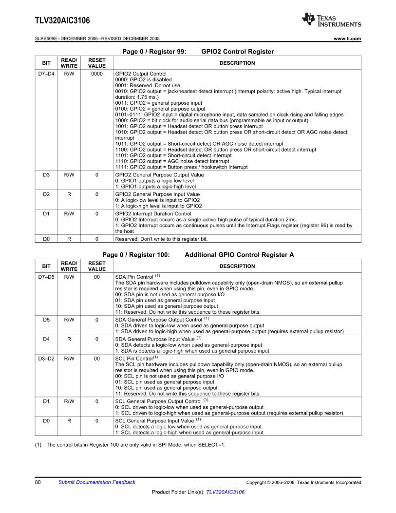
TLV320AIC3106
SLAS509E–DECEMBER 2006–REVISED DECEMBER 2008........................................................................................................................................ www.ti.com
Page 0 / Register 99: GPIO2 Control RegisterREAD/ RESETBIT DESCRIPTIONWRITE VALUE
D7–D4 R/W 0000 GPIO2 Output Control0000: GPIO2 is disabled0001: Reserved. Do not use.0010: GPIO2 output = jack/headset detect interrupt (interrupt polarity: active high. Typical interruptduration: 1.75 ms.)0011: GPIO2 = general purpose input0100: GPIO2 = general purpose output0101–0111: GPIO2 input = digital microphone input, data sampled on clock rising and falling edges1000: GPIO2 = bit clock for audio serial data bus (programmable as input or output)1001: GPIO2 output = Headset detect OR button press interrupt1010: GPIO2 output = Headset detect OR button press OR short-circuit detect OR AGC noise detectinterrupt1011: GPIO2 output = Short-circuit detect OR AGC noise detect interrupt1100: GPIO2 output = Headset detect OR button press OR short-circuit detect interrupt1101: GPIO2 output = Short-circuit detect interrupt1110: GPIO2 output = AGC noise detect interrupt1111: GPIO2 output = Button press / hookswitch interrupt
D3 R/W 0 GPIO2 General Purpose Output Value0: GPIO1 outputs a logic-low level1: GPIO1 outputs a logic-high level
D2 R 0 GPIO2 General Purpose Input Value0: A logic-low level is input to GPIO21: A logic-high level is input to GPIO2
D1 R/W 0 GPIO2 Interrupt Duration Control0: GPIO2 Interrupt occurs as a single active-high pulse of typical duration 2ms.1: GPIO2 Interrupt occurs as continuous pulses until the Interrupt Flags register (register 96) is read bythe host
D0 R 0 Reserved. Don’t write to this register bit.
Page 0 / Register 100: Additional GPIO Control Register AREAD/ RESETBIT DESCRIPTIONWRITE VALUE
D7–D6 R/W 00 SDA Pin Control (1)The SDA pin hardware includes pulldown capability only (open-drain NMOS), so an external pullupresistor is required when using this pin, even in GPIO mode.00: SDA pin is not used as general purpose I/O01: SDA pin used as general purpose input10: SDA pin used as general purpose output11: Reserved. Do not write this sequence to these register bits.
D5 R/W 0 SDA General Purpose Output Control (1)0: SDA driven to logic-low when used as general-purpose output1: SDA driven to logic-high when used as general-purpose output (requires external pullup resistor)
D4 R 0 SDA General Purpose Input Value (1)
0: SDA detects a logic-low when used as general-purpose input1: SDA is detects a logic-high when used as general purpose input
D3–D2 R/W 00 SCL Pin Control(1)The SCL pin hardware includes pulldown capability only (open-drain NMOS), so an external pullupresistor is required when using this pin, even in GPIO mode.00: SCL pin is not used as general purpose I/O01: SCL pin used as general purpose input10: SCL pin used as general purpose output11: Reserved. Do not write this sequence to these register bits.
D1 R/W 0 SCL General Purpose Output Control (1)0: SCL driven to logic-low when used as general-purpose output1: SCL driven to logic-high when used as general-purpose output (requires external pullup resistor)
D0 R 0 SCL General Purpose Input Value (1)
0: SCL detects a logic-low when used as general-purpose input1: SCL detects a logic-high when used as general-purpose input
(1) The control bits in Register 100 are only valid in SPI Mode, when SELECT=1.
80 Submit Documentation Feedback Copyright © 2006–2008, Texas Instruments Incorporated
Product Folder Link(s): TLV320AIC3106
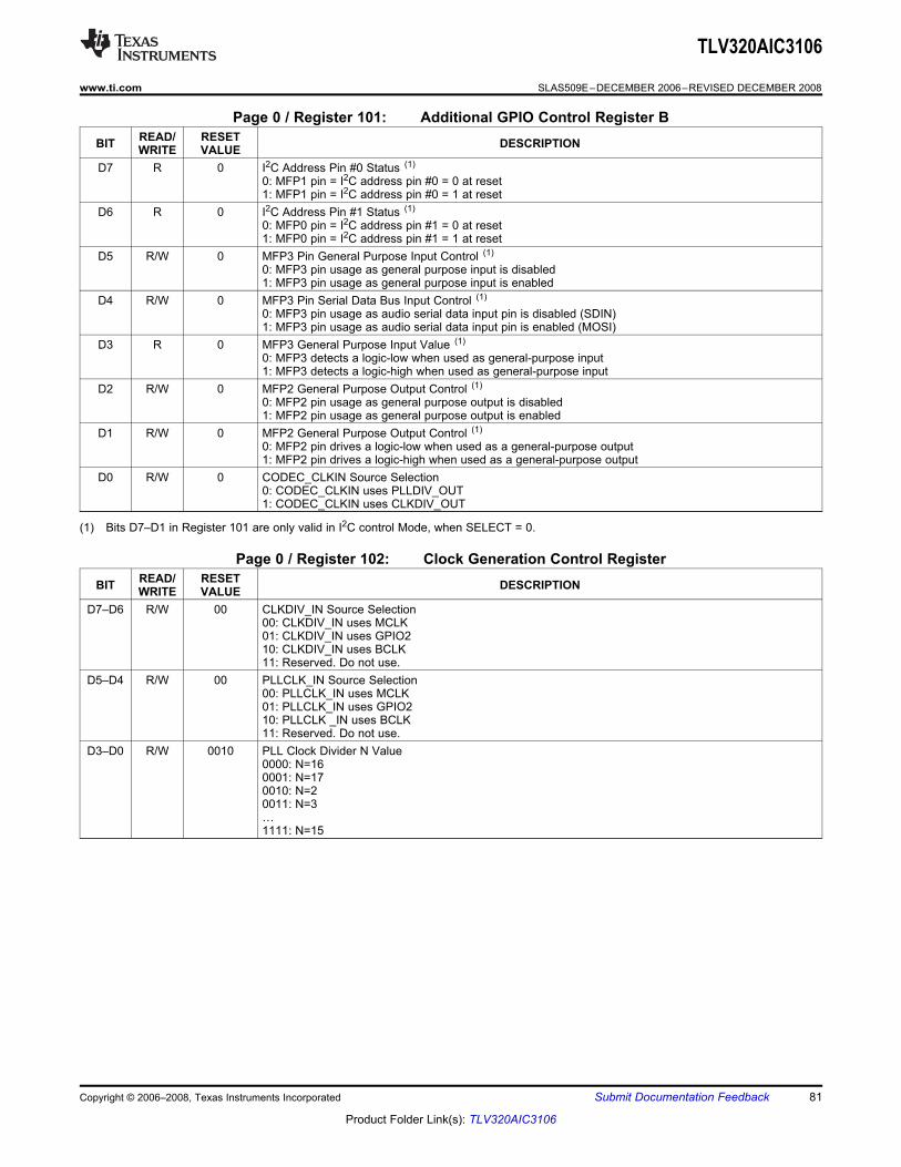
TLV320AIC3106
www.ti.com ........................................................................................................................................ SLAS509E–DECEMBER 2006–REVISED DECEMBER 2008
Page 0 / Register 101: Additional GPIO Control Register BREAD/ RESETBIT DESCRIPTIONWRITE VALUE
D7 R 0 I2C Address Pin #0 Status (1)0: MFP1 pin = I2C address pin #0 = 0 at reset1: MFP1 pin = I2C address pin #0 = 1 at reset
D6 R 0 I2C Address Pin #1 Status (1)0: MFP0 pin = I2C address pin #1 = 0 at reset1: MFP0 pin = I2C address pin #1 = 1 at reset
D5 R/W 0 MFP3 Pin General Purpose Input Control (1)0: MFP3 pin usage as general purpose input is disabled1: MFP3 pin usage as general purpose input is enabled
D4 R/W 0 MFP3 Pin Serial Data Bus Input Control (1)0: MFP3 pin usage as audio serial data input pin is disabled (SDIN)1: MFP3 pin usage as audio serial data input pin is enabled (MOSI)
D3 R 0 MFP3 General Purpose Input Value (1)
0: MFP3 detects a logic-low when used as general-purpose input1: MFP3 detects a logic-high when used as general-purpose input
D2 R/W 0 MFP2 General Purpose Output Control (1)0: MFP2 pin usage as general purpose output is disabled1: MFP2 pin usage as general purpose output is enabled
D1 R/W 0 MFP2 General Purpose Output Control (1)0: MFP2 pin drives a logic-low when used as a general-purpose output1: MFP2 pin drives a logic-high when used as a general-purpose output
D0 R/W 0 CODEC_CLKIN Source Selection0: CODEC_CLKIN uses PLLDIV_OUT1: CODEC_CLKIN uses CLKDIV_OUT
(1) Bits D7–D1 in Register 101 are only valid in I2C control Mode, when SELECT = 0.
Page 0 / Register 102: Clock Generation Control RegisterREAD/ RESETBIT DESCRIPTIONWRITE VALUE
D7–D6 R/W 00 CLKDIV_IN Source Selection00: CLKDIV_IN uses MCLK01: CLKDIV_IN uses GPIO210: CLKDIV_IN uses BCLK11: Reserved. Do not use.
D5–D4 R/W 00 PLLCLK_IN Source Selection00: PLLCLK_IN uses MCLK01: PLLCLK_IN uses GPIO210: PLLCLK _IN uses BCLK11: Reserved. Do not use.
D3–D0 R/W 0010 PLL Clock Divider N Value0000: N=160001: N=170010: N=20011: N=3…1111: N=15
Copyright © 2006–2008, Texas Instruments Incorporated Submit Documentation Feedback 81
Product Folder Link(s): TLV320AIC3106
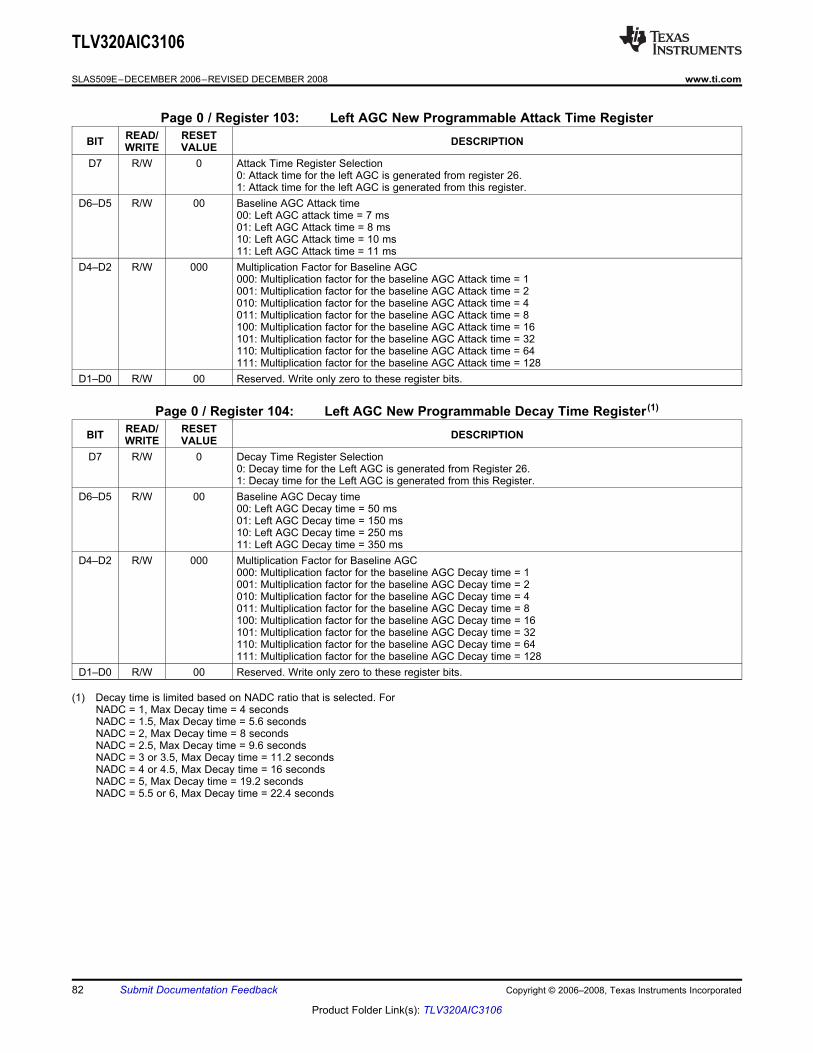
TLV320AIC3106
SLAS509E–DECEMBER 2006–REVISED DECEMBER 2008........................................................................................................................................ www.ti.com
Page 0 / Register 103: Left AGC New Programmable Attack Time RegisterREAD/ RESETBIT DESCRIPTIONWRITE VALUE
D7 R/W 0 Attack Time Register Selection0: Attack time for the left AGC is generated from register 26.1: Attack time for the left AGC is generated from this register.
D6–D5 R/W 00 Baseline AGC Attack time00: Left AGC attack time = 7 ms01: Left AGC Attack time = 8 ms10: Left AGC Attack time = 10 ms11: Left AGC Attack time = 11 ms
D4–D2 R/W 000 Multiplication Factor for Baseline AGC000: Multiplication factor for the baseline AGC Attack time = 1001: Multiplication factor for the baseline AGC Attack time = 2010: Multiplication factor for the baseline AGC Attack time = 4011: Multiplication factor for the baseline AGC Attack time = 8100: Multiplication factor for the baseline AGC Attack time = 16101: Multiplication factor for the baseline AGC Attack time = 32110: Multiplication factor for the baseline AGC Attack time = 64111: Multiplication factor for the baseline AGC Attack time = 128
D1–D0 R/W 00 Reserved. Write only zero to these register bits.
Page 0 / Register 104: Left AGC New Programmable Decay Time Register(1)READ/ RESETBIT DESCRIPTIONWRITE VALUE
D7 R/W 0 Decay Time Register Selection0: Decay time for the Left AGC is generated from Register 26.1: Decay time for the Left AGC is generated from this Register.
D6–D5 R/W 00 Baseline AGC Decay time00: Left AGC Decay time = 50 ms01: Left AGC Decay time = 150 ms10: Left AGC Decay time = 250 ms11: Left AGC Decay time = 350 ms
D4–D2 R/W 000 Multiplication Factor for Baseline AGC000: Multiplication factor for the baseline AGC Decay time = 1001: Multiplication factor for the baseline AGC Decay time = 2010: Multiplication factor for the baseline AGC Decay time = 4011: Multiplication factor for the baseline AGC Decay time = 8100: Multiplication factor for the baseline AGC Decay time = 16101: Multiplication factor for the baseline AGC Decay time = 32110: Multiplication factor for the baseline AGC Decay time = 64111: Multiplication factor for the baseline AGC Decay time = 128
D1–D0 R/W 00 Reserved. Write only zero to these register bits.
(1) Decay time is limited based on NADC ratio that is selected. ForNADC = 1, Max Decay time = 4 secondsNADC = 1.5, Max Decay time = 5.6 secondsNADC = 2, Max Decay time = 8 secondsNADC = 2.5, Max Decay time = 9.6 secondsNADC = 3 or 3.5, Max Decay time = 11.2 secondsNADC = 4 or 4.5, Max Decay time = 16 secondsNADC = 5, Max Decay time = 19.2 secondsNADC = 5.5 or 6, Max Decay time = 22.4 seconds
82 Submit Documentation Feedback Copyright © 2006–2008, Texas Instruments Incorporated
Product Folder Link(s): TLV320AIC3106
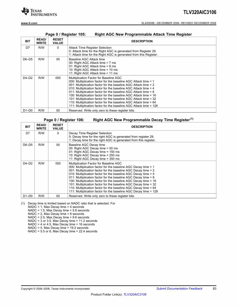
TLV320AIC3106
www.ti.com ........................................................................................................................................ SLAS509E–DECEMBER 2006–REVISED DECEMBER 2008
Page 0 / Register 105: Right AGC New Programmable Attack Time RegisterREAD/ RESETBIT DESCRIPTIONWRITE VALUE
D7 R/W 0 Attack Time Register Selection0: Attack time for the Right AGC is generated from Register 29.1: Attack time for the Right AGC is generated from this Register.
D6–D5 R/W 00 Baseline AGC Attack time00: Right AGC Attack time = 7 ms01: Right AGC Attack time = 8 ms10: Right AGC Attack time = 10 ms11: Right AGC Attack time = 11 ms
D4–D2 R/W 000 Multiplication Factor for Baseline AGC000: Multiplication factor for the baseline AGC Attack time = 1001: Multiplication factor for the baseline AGC Attack time = 2010: Multiplication factor for the baseline AGC Attack time = 4011: Multiplication factor for the baseline AGC Attack time = 8100: Multiplication factor for the baseline AGC Attack time = 16101: Multiplication factor for the baseline AGC Attack time = 32110: Multiplication factor for the baseline AGC Attack time = 64111: Multiplication factor for the baseline AGC Attack time = 128
D1–D0 R/W 00 Reserved. Write only zero to these register bits.
Page 0 / Register 106: Right AGC New Programmable Decay Time Register(1)READ/ RESETBIT DESCRIPTIONWRITE VALUE
D7 R/W 0 Decay Time Register Selection0: Decay time for the right AGC is generated from register 29.1: Decay time for the right AGC is generated from this register.
D6–D5 R/W 00 Baseline AGC Decay time00: Right AGC Decay time = 50 ms01: Right AGC Decay time = 150 ms10: Right AGC Decay time = 250 ms11: Right AGC Decay time = 350 ms
D4–D2 R/W 000 Multiplication Factor for Baseline AGC000: Multiplication factor for the baseline AGC Decay time = 1001: Multiplication factor for the baseline AGC Decay time = 2010: Multiplication factor for the baseline AGC Decay time = 4011: Multiplication factor for the baseline AGC Decay time = 8100: Multiplication factor for the baseline AGC Decay time = 16101: Multiplication factor for the baseline AGC Decay time = 32110: Multiplication factor for the baseline AGC Decay time = 64111: Multiplication factor for the baseline AGC Decay time = 128
D1–D0 R/W 00 Reserved. Write only zero to these register bits.
(1) Decay time is limited based on NADC ratio that is selected. ForNADC = 1, Max Decay time = 4 secondsNADC = 1.5, Max Decay time = 5.6 secondsNADC = 2, Max Decay time = 8 secondsNADC = 2.5, Max Decay time = 9.6 secondsNADC = 3 or 3.5, Max Decay time = 11.2 secondsNADC = 4 or 4.5, Max Decay time = 16 secondsNADC = 5, Max Decay time = 19.2 secondsNADC = 5.5 or 6, Max Decay time = 22.4 seconds
Copyright © 2006–2008, Texas Instruments Incorporated Submit Documentation Feedback 83
Product Folder Link(s): TLV320AIC3106
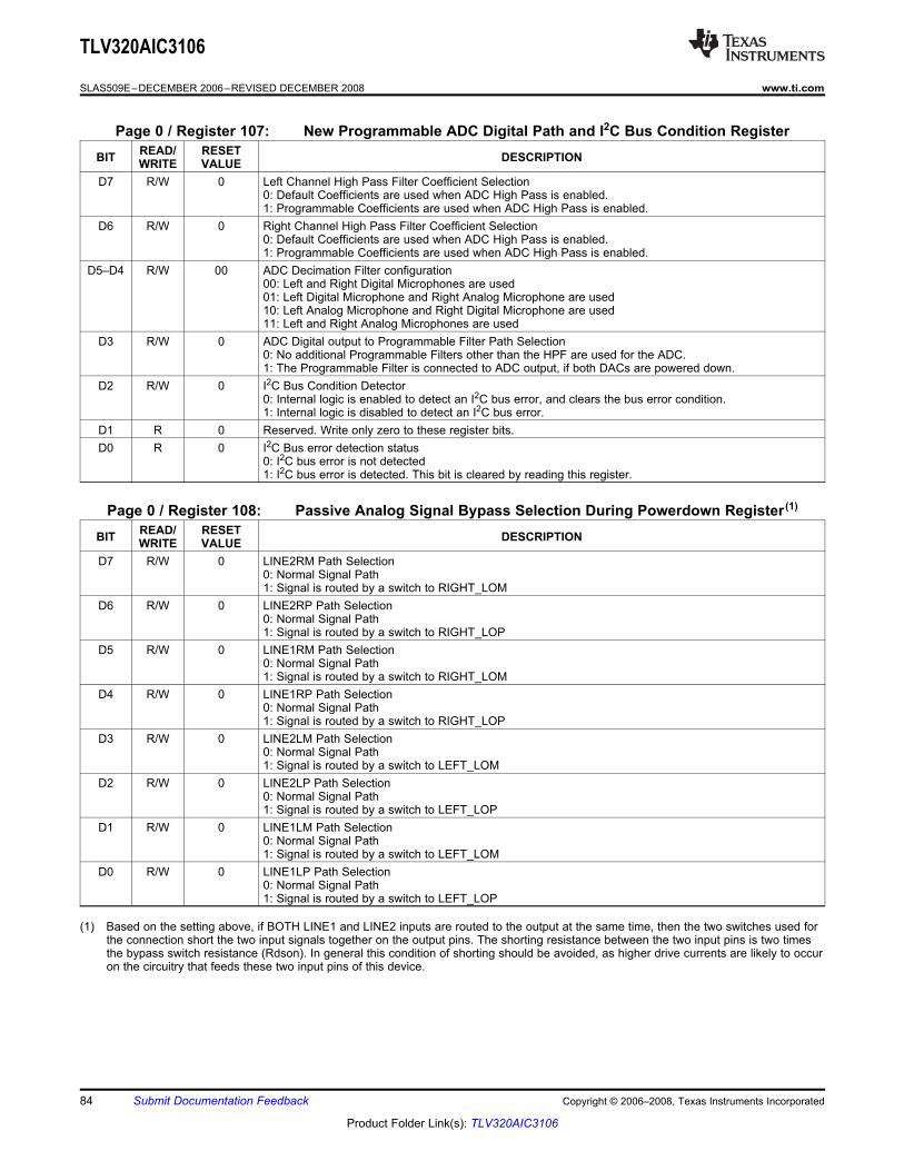
TLV320AIC3106
SLAS509E–DECEMBER 2006–REVISED DECEMBER 2008........................................................................................................................................ www.ti.com
Page 0 / Register 107: New Programmable ADC Digital Path and I2C Bus Condition RegisterREAD/ RESETBIT DESCRIPTIONWRITE VALUE
D7 R/W 0 Left Channel High Pass Filter Coefficient Selection0: Default Coefficients are used when ADC High Pass is enabled.1: Programmable Coefficients are used when ADC High Pass is enabled.
D6 R/W 0 Right Channel High Pass Filter Coefficient Selection0: Default Coefficients are used when ADC High Pass is enabled.1: Programmable Coefficients are used when ADC High Pass is enabled.
D5–D4 R/W 00 ADC Decimation Filter configuration00: Left and Right Digital Microphones are used01: Left Digital Microphone and Right Analog Microphone are used10: Left Analog Microphone and Right Digital Microphone are used11: Left and Right Analog Microphones are used
D3 R/W 0 ADC Digital output to Programmable Filter Path Selection0: No additional Programmable Filters other than the HPF are used for the ADC.1: The Programmable Filter is connected to ADC output, if both DACs are powered down.
D2 R/W 0 I2C Bus Condition Detector0: Internal logic is enabled to detect an I2C bus error, and clears the bus error condition.1: Internal logic is disabled to detect an I2C bus error.
D1 R 0 Reserved. Write only zero to these register bits.D0 R 0 I2C Bus error detection status
0: I2C bus error is not detected1: I2C bus error is detected. This bit is cleared by reading this register.
Page 0 / Register 108: Passive Analog Signal Bypass Selection During Powerdown Register(1)READ/ RESETBIT DESCRIPTIONWRITE VALUE
D7 R/W 0 LINE2RM Path Selection0: Normal Signal Path1: Signal is routed by a switch to RIGHT_LOM
D6 R/W 0 LINE2RP Path Selection0: Normal Signal Path1: Signal is routed by a switch to RIGHT_LOP
D5 R/W 0 LINE1RM Path Selection0: Normal Signal Path1: Signal is routed by a switch to RIGHT_LOM
D4 R/W 0 LINE1RP Path Selection0: Normal Signal Path1: Signal is routed by a switch to RIGHT_LOP
D3 R/W 0 LINE2LM Path Selection0: Normal Signal Path1: Signal is routed by a switch to LEFT_LOM
D2 R/W 0 LINE2LP Path Selection0: Normal Signal Path1: Signal is routed by a switch to LEFT_LOP
D1 R/W 0 LINE1LM Path Selection0: Normal Signal Path1: Signal is routed by a switch to LEFT_LOM
D0 R/W 0 LINE1LP Path Selection0: Normal Signal Path1: Signal is routed by a switch to LEFT_LOP
(1) Based on the setting above, if BOTH LINE1 and LINE2 inputs are routed to the output at the same time, then the two switches used forthe connection short the two input signals together on the output pins. The shorting resistance between the two input pins is two timesthe bypass switch resistance (Rdson). In general this condition of shorting should be avoided, as higher drive currents are likely to occuron the circuitry that feeds these two input pins of this device.
84 Submit Documentation Feedback Copyright © 2006–2008, Texas Instruments Incorporated
Product Folder Link(s): TLV320AIC3106

TLV320AIC3106
www.ti.com ........................................................................................................................................ SLAS509E–DECEMBER 2006–REVISED DECEMBER 2008
Page 0 / Register 109: DAC Quiescent Current Adjustment RegisterREAD/ RESETBIT DESCRIPTIONWRITE VALUE
D7–D6 R/W 00 DAC Current Adjustment00: Default01: 50% increase in DAC reference current10: Reserved11: 100% increase in DAC reference current
D5–D0 R/W 00 0000 Reserved. Write only zero to these register bits.
Page 0 / Register 110–127: Reserved RegistersREAD/ RESETBIT DESCRIPTIONWRITE VALUE
D7–D0 R 0000 0000 Reserved. Do not write to these registers.
Page 1 / Register 0: Page Select RegisterREAD/ RESETBIT DESCRIPTIONWRITE VALUE
D7–D1 X 0000 000 Reserved, write only zeros to these register bitsD0 R/W 0 Page Select Bit
Writing zero to this bit sets Page-0 as the active page for following register accesses. Writing a one tothis bit sets Page-1 as the active page for following register accesses. It is recommended that the userread this register bit back after each write, to ensure that the proper page is being accessed for futureregister read/writes. This register has the same functionality on page-0 and page-1.
Page 1 / Register 1: Left Channel Audio Effects Filter N0 Coefficient MSB Register(1)
READ/ RESETBIT DESCRIPTIONWRITE VALUED7–D0 R/W 0110 1011 Left Channel Audio Effects Filter N0 Coefficient MSB
The 16-bit integer contained in the MSB and LSB registers for this coefficient are interpreted as a2s-complement integer, with possible values ranging from –32768 to 32767.
(1) When programming any coefficient value in Page 1, the MSB register should always be written first, immediately followed by the LSBregister. Even if only the MSB or LSB of the coefficient changes, both registers should be written in this sequence.
Page 1 / Register 2: Left Channel Audio Effects Filter N0 Coefficient LSB RegisterREAD/ RESETBIT DESCRIPTIONWRITE VALUE
D7–D0 R/W 1110 0011 Left Channel Audio Effects Filter N0 Coefficient LSBThe 16-bit integer contained in the MSB and LSB registers for this coefficient are interpreted as a2s-complement integer, with possible values ranging from –32768 to 32767.
Page 1 / Register 3: Left Channel Audio Effects Filter N1 Coefficient MSB RegisterREAD/ RESETBIT DESCRIPTIONWRITE VALUE
D7–D0 R/W 1001 0110 Left Channel Audio Effects Filter N1 Coefficient MSBThe 16-bit integer contained in the MSB and LSB registers for this coefficient are interpreted as a2s-complement integer, with possible values ranging from –32768 to 32767.
Page 1 / Register 4: Left Channel Audio Effects Filter N1 Coefficient LSB RegisterREAD/ RESETBIT DESCRIPTIONWRITE VALUE
D7–D0 R/W 0110 0110 Left Channel Audio Effects Filter N1 Coefficient LSBThe 16-bit integer contained in the MSB and LSB registers for this coefficient are interpreted as a2s-complement integer, with possible values ranging from –32768 to 32767.
Copyright © 2006–2008, Texas Instruments Incorporated Submit Documentation Feedback 85
Product Folder Link(s): TLV320AIC3106
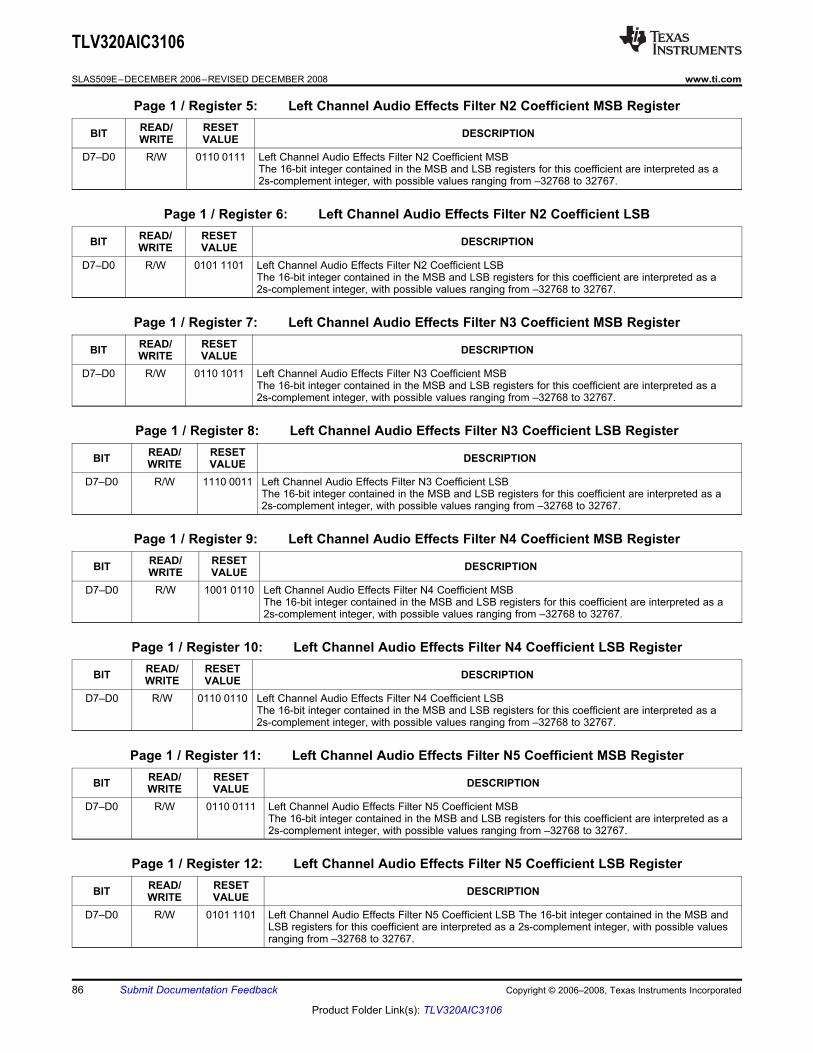
TLV320AIC3106
SLAS509E–DECEMBER 2006–REVISED DECEMBER 2008........................................................................................................................................ www.ti.com
Page 1 / Register 5: Left Channel Audio Effects Filter N2 Coefficient MSB RegisterREAD/ RESETBIT DESCRIPTIONWRITE VALUE
D7–D0 R/W 0110 0111 Left Channel Audio Effects Filter N2 Coefficient MSBThe 16-bit integer contained in the MSB and LSB registers for this coefficient are interpreted as a2s-complement integer, with possible values ranging from –32768 to 32767.
Page 1 / Register 6: Left Channel Audio Effects Filter N2 Coefficient LSBREAD/ RESETBIT DESCRIPTIONWRITE VALUE
D7–D0 R/W 0101 1101 Left Channel Audio Effects Filter N2 Coefficient LSBThe 16-bit integer contained in the MSB and LSB registers for this coefficient are interpreted as a2s-complement integer, with possible values ranging from –32768 to 32767.
Page 1 / Register 7: Left Channel Audio Effects Filter N3 Coefficient MSB RegisterREAD/ RESETBIT DESCRIPTIONWRITE VALUE
D7–D0 R/W 0110 1011 Left Channel Audio Effects Filter N3 Coefficient MSBThe 16-bit integer contained in the MSB and LSB registers for this coefficient are interpreted as a2s-complement integer, with possible values ranging from –32768 to 32767.
Page 1 / Register 8: Left Channel Audio Effects Filter N3 Coefficient LSB RegisterREAD/ RESETBIT DESCRIPTIONWRITE VALUE
D7–D0 R/W 1110 0011 Left Channel Audio Effects Filter N3 Coefficient LSBThe 16-bit integer contained in the MSB and LSB registers for this coefficient are interpreted as a2s-complement integer, with possible values ranging from –32768 to 32767.
Page 1 / Register 9: Left Channel Audio Effects Filter N4 Coefficient MSB RegisterREAD/ RESETBIT DESCRIPTIONWRITE VALUE
D7–D0 R/W 1001 0110 Left Channel Audio Effects Filter N4 Coefficient MSBThe 16-bit integer contained in the MSB and LSB registers for this coefficient are interpreted as a2s-complement integer, with possible values ranging from –32768 to 32767.
Page 1 / Register 10: Left Channel Audio Effects Filter N4 Coefficient LSB RegisterREAD/ RESETBIT DESCRIPTIONWRITE VALUE
D7–D0 R/W 0110 0110 Left Channel Audio Effects Filter N4 Coefficient LSBThe 16-bit integer contained in the MSB and LSB registers for this coefficient are interpreted as a2s-complement integer, with possible values ranging from –32768 to 32767.
Page 1 / Register 11: Left Channel Audio Effects Filter N5 Coefficient MSB RegisterREAD/ RESETBIT DESCRIPTIONWRITE VALUE
D7–D0 R/W 0110 0111 Left Channel Audio Effects Filter N5 Coefficient MSBThe 16-bit integer contained in the MSB and LSB registers for this coefficient are interpreted as a2s-complement integer, with possible values ranging from –32768 to 32767.
Page 1 / Register 12: Left Channel Audio Effects Filter N5 Coefficient LSB RegisterREAD/ RESETBIT DESCRIPTIONWRITE VALUE
D7–D0 R/W 0101 1101 Left Channel Audio Effects Filter N5 Coefficient LSB The 16-bit integer contained in the MSB andLSB registers for this coefficient are interpreted as a 2s-complement integer, with possible valuesranging from –32768 to 32767.
86 Submit Documentation Feedback Copyright © 2006–2008, Texas Instruments Incorporated
Product Folder Link(s): TLV320AIC3106
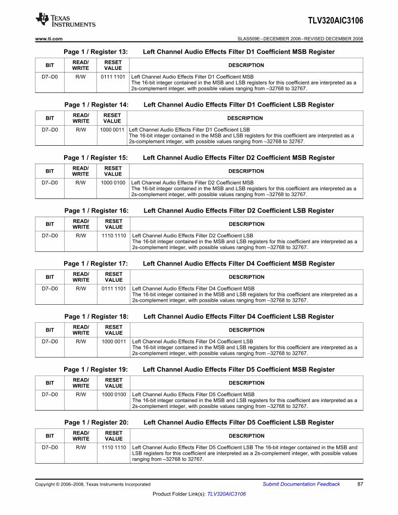
TLV320AIC3106
www.ti.com ........................................................................................................................................ SLAS509E–DECEMBER 2006–REVISED DECEMBER 2008
Page 1 / Register 13: Left Channel Audio Effects Filter D1 Coefficient MSB RegisterREAD/ RESETBIT DESCRIPTIONWRITE VALUE
D7–D0 R/W 0111 1101 Left Channel Audio Effects Filter D1 Coefficient MSBThe 16-bit integer contained in the MSB and LSB registers for this coefficient are interpreted as a2s-complement integer, with possible values ranging from –32768 to 32767.
Page 1 / Register 14: Left Channel Audio Effects Filter D1 Coefficient LSB RegisterREAD/ RESETBIT DESCRIPTIONWRITE VALUE
D7–D0 R/W 1000 0011 Left Channel Audio Effects Filter D1 Coefficient LSBThe 16-bit integer contained in the MSB and LSB registers for this coefficient are interpreted as a2s-complement integer, with possible values ranging from –32768 to 32767.
Page 1 / Register 15: Left Channel Audio Effects Filter D2 Coefficient MSB RegisterREAD/ RESETBIT DESCRIPTIONWRITE VALUE
D7–D0 R/W 1000 0100 Left Channel Audio Effects Filter D2 Coefficient MSBThe 16-bit integer contained in the MSB and LSB registers for this coefficient are interpreted as a2s-complement integer, with possible values ranging from –32768 to 32767.
Page 1 / Register 16: Left Channel Audio Effects Filter D2 Coefficient LSB RegisterREAD/ RESETBIT DESCRIPTIONWRITE VALUE
D7–D0 R/W 1110 1110 Left Channel Audio Effects Filter D2 Coefficient LSBThe 16-bit integer contained in the MSB and LSB registers for this coefficient are interpreted as a2s-complement integer, with possible values ranging from –32768 to 32767.
Page 1 / Register 17: Left Channel Audio Effects Filter D4 Coefficient MSB RegisterREAD/ RESETBIT DESCRIPTIONWRITE VALUE
D7–D0 R/W 0111 1101 Left Channel Audio Effects Filter D4 Coefficient MSBThe 16-bit integer contained in the MSB and LSB registers for this coefficient are interpreted as a2s-complement integer, with possible values ranging from –32768 to 32767.
Page 1 / Register 18: Left Channel Audio Effects Filter D4 Coefficient LSB RegisterREAD/ RESETBIT DESCRIPTIONWRITE VALUE
D7–D0 R/W 1000 0011 Left Channel Audio Effects Filter D4 Coefficient LSBThe 16-bit integer contained in the MSB and LSB registers for this coefficient are interpreted as a2s-complement integer, with possible values ranging from –32768 to 32767.
Page 1 / Register 19: Left Channel Audio Effects Filter D5 Coefficient MSB RegisterREAD/ RESETBIT DESCRIPTIONWRITE VALUE
D7–D0 R/W 1000 0100 Left Channel Audio Effects Filter D5 Coefficient MSBThe 16-bit integer contained in the MSB and LSB registers for this coefficient are interpreted as a2s-complement integer, with possible values ranging from –32768 to 32767.
Page 1 / Register 20: Left Channel Audio Effects Filter D5 Coefficient LSB RegisterREAD/ RESETBIT DESCRIPTIONWRITE VALUE
D7–D0 R/W 1110 1110 Left Channel Audio Effects Filter D5 Coefficient LSB The 16-bit integer contained in the MSB andLSB registers for this coefficient are interpreted as a 2s-complement integer, with possible valuesranging from –32768 to 32767.
Copyright © 2006–2008, Texas Instruments Incorporated Submit Documentation Feedback 87
Product Folder Link(s): TLV320AIC3106

TLV320AIC3106
SLAS509E–DECEMBER 2006–REVISED DECEMBER 2008........................................................................................................................................ www.ti.com
Page 1 / Register 21: Left Channel De-Emphasis Filter N0 Coefficient MSB RegisterREAD/ RESETBIT DESCRIPTIONWRITE VALUE
D7–D0 R/W 0011 1001 Left Channel De-Emphasis Filter N0 Coefficient MSB The 16-bit integer contained in the MSB andLSB registers for this coefficient are interpreted as a 2s-complement integer, with possible valuesranging from –32768 to 32767.
Page 1 / Register 22: Left Channel De-Emphasis Filter N0 Coefficient LSB RegisterREAD/ RESETBIT DESCRIPTIONWRITE VALUE
D7–D0 R/W 0101 0101 Left Channel De-Emphasis Filter N0 Coefficient LSB The 16-bit integer contained in the MSB andLSB registers for this coefficient are interpreted as a 2s-complement integer, with possible valuesranging from –32768 to 32767.
Page 1 / Register 23: Left Channel De-Emphasis Filter N1 Coefficient MSB RegisterREAD/ RESETBIT DESCRIPTIONWRITE VALUE
D7–D0 R/W 1111 0011 Left Channel De-Emphasis Filter N1 Coefficient MSB The 16-bit integer contained in the MSB andLSB registers for this coefficient are interpreted as a 2s-complement integer, with possible valuesranging from –32768 to 32767.
Page 1 / Register 24: Left Channel De-Emphasis Filter N1 Coefficient LSB RegisterREAD/ RESETBIT DESCRIPTIONWRITE VALUE
D7–D0 R/W 0010 1101 Left Channel De-Emphasis Filter N1 Coefficient LSB The 16-bit integer contained in the MSB andLSB registers for this coefficient are interpreted as a 2s-complement integer, with possible valuesranging from –32768 to 32767.
Page 1 / Register 25: Left Channel De-Emphasis Filter D1 Coefficient MSB RegisterREAD/ RESETBIT DESCRIPTIONWRITE VALUE
D7–D0 R/W 0101 0011 Left Channel De-Emphasis Filter D1 Coefficient MSB The 16-bit integer contained in the MSB andLSB registers for this coefficient are interpreted as a 2s-complement integer, with possible valuesranging from –32768 to 32767.
Page 1 / Register 26: Left Channel De-Emphasis Filter D1 Coefficient LSB RegisterREAD/ RESETBIT DESCRIPTIONWRITE VALUE
D7–D0 R/W 0111 1110 Left Channel De-Emphasis Filter D1 Coefficient LSB The 16-bit integer contained in the MSB andLSB registers for this coefficient are interpreted as a 2s-complement integer, with possible valuesranging from –32768 to 32767.
Page 1 / Register 27: Right Channel Audio Effects Filter N0 Coefficient MSB RegisterREAD/ RESETBIT DESCRIPTIONWRITE VALUE
D7–D0 R/W 0110 1011 Right Channel Audio Effects Filter N0 Coefficient MSB The 16-bit integer contained in the MSB andLSB registers for this coefficient are interpreted as a 2s-complement integer, with possible valuesranging from –32768 to 32767.
Page 1 / Register 28: Right Channel Audio Effects Filter N0 Coefficient LSB RegisterREAD/ RESETBIT DESCRIPTIONWRITE VALUE
D7–D0 R/W 1110 0011 Right Channel Audio Effects Filter N0 Coefficient LSB The 16-bit integer contained in the MSB andLSB registers for this coefficient are interpreted as a 2s-complement integer, with possible valuesranging from –32768 to 32767.
88 Submit Documentation Feedback Copyright © 2006–2008, Texas Instruments Incorporated
Product Folder Link(s): TLV320AIC3106
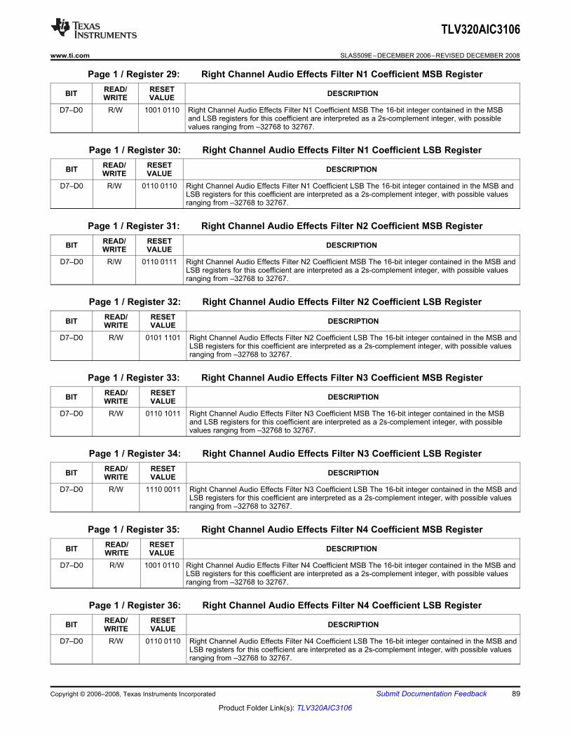
TLV320AIC3106
www.ti.com ........................................................................................................................................ SLAS509E–DECEMBER 2006–REVISED DECEMBER 2008
Page 1 / Register 29: Right Channel Audio Effects Filter N1 Coefficient MSB RegisterREAD/ RESETBIT DESCRIPTIONWRITE VALUE
D7–D0 R/W 1001 0110 Right Channel Audio Effects Filter N1 Coefficient MSB The 16-bit integer contained in the MSBand LSB registers for this coefficient are interpreted as a 2s-complement integer, with possiblevalues ranging from –32768 to 32767.
Page 1 / Register 30: Right Channel Audio Effects Filter N1 Coefficient LSB RegisterREAD/ RESETBIT DESCRIPTIONWRITE VALUE
D7–D0 R/W 0110 0110 Right Channel Audio Effects Filter N1 Coefficient LSB The 16-bit integer contained in the MSB andLSB registers for this coefficient are interpreted as a 2s-complement integer, with possible valuesranging from –32768 to 32767.
Page 1 / Register 31: Right Channel Audio Effects Filter N2 Coefficient MSB RegisterREAD/ RESETBIT DESCRIPTIONWRITE VALUE
D7–D0 R/W 0110 0111 Right Channel Audio Effects Filter N2 Coefficient MSB The 16-bit integer contained in the MSB andLSB registers for this coefficient are interpreted as a 2s-complement integer, with possible valuesranging from –32768 to 32767.
Page 1 / Register 32: Right Channel Audio Effects Filter N2 Coefficient LSB RegisterREAD/ RESETBIT DESCRIPTIONWRITE VALUE
D7–D0 R/W 0101 1101 Right Channel Audio Effects Filter N2 Coefficient LSB The 16-bit integer contained in the MSB andLSB registers for this coefficient are interpreted as a 2s-complement integer, with possible valuesranging from –32768 to 32767.
Page 1 / Register 33: Right Channel Audio Effects Filter N3 Coefficient MSB RegisterREAD/ RESETBIT DESCRIPTIONWRITE VALUE
D7–D0 R/W 0110 1011 Right Channel Audio Effects Filter N3 Coefficient MSB The 16-bit integer contained in the MSBand LSB registers for this coefficient are interpreted as a 2s-complement integer, with possiblevalues ranging from –32768 to 32767.
Page 1 / Register 34: Right Channel Audio Effects Filter N3 Coefficient LSB RegisterREAD/ RESETBIT DESCRIPTIONWRITE VALUE
D7–D0 R/W 1110 0011 Right Channel Audio Effects Filter N3 Coefficient LSB The 16-bit integer contained in the MSB andLSB registers for this coefficient are interpreted as a 2s-complement integer, with possible valuesranging from –32768 to 32767.
Page 1 / Register 35: Right Channel Audio Effects Filter N4 Coefficient MSB RegisterREAD/ RESETBIT DESCRIPTIONWRITE VALUE
D7–D0 R/W 1001 0110 Right Channel Audio Effects Filter N4 Coefficient MSB The 16-bit integer contained in the MSB andLSB registers for this coefficient are interpreted as a 2s-complement integer, with possible valuesranging from –32768 to 32767.
Page 1 / Register 36: Right Channel Audio Effects Filter N4 Coefficient LSB RegisterREAD/ RESETBIT DESCRIPTIONWRITE VALUE
D7–D0 R/W 0110 0110 Right Channel Audio Effects Filter N4 Coefficient LSB The 16-bit integer contained in the MSB andLSB registers for this coefficient are interpreted as a 2s-complement integer, with possible valuesranging from –32768 to 32767.
Copyright © 2006–2008, Texas Instruments Incorporated Submit Documentation Feedback 89
Product Folder Link(s): TLV320AIC3106
TLV320AIC3106
SLAS509E–DECEMBER 2006–REVISED DECEMBER 2008........................................................................................................................................ www.ti.com
Page 1 / Register 37: Right Channel Audio Effects Filter N5 Coefficient MSB RegisterREAD/ RESETBIT DESCRIPTIONWRITE VALUE
D7–D0 R/W 0110 0111 Right Channel Audio Effects Filter N5 Coefficient MSB The 16-bit integer contained in the MSBand LSB registers for this coefficient are interpreted as a 2s-complement integer, with possiblevalues ranging from –32768 to 32767.
Page 1 / Register 38: Right Channel Audio Effects Filter N5 Coefficient LSB RegisterREAD/ RESETBIT DESCRIPTIONWRITE VALUE
D7–D0 R/W 0101 1101 Right Channel Audio Effects Filter N5 Coefficient LSB The 16-bit integer contained in the MSB andLSB registers for this coefficient are interpreted as a 2s-complement integer, with possible valuesranging from –32768 to 32767.
Page 1 / Register 39: Right Channel Audio Effects Filter D1 Coefficient MSB RegisterREAD/ RESETBIT DESCRIPTIONWRITE VALUE
D7–D0 R/W 0111 1101 Right Channel Audio Effects Filter D1 Coefficient MSB The 16-bit integer contained in the MSBand LSB registers for this coefficient are interpreted as a 2s-complement integer, with possiblevalues ranging from –32768 to 32767.
Page 1 / Register 40: Right Channel Audio Effects Filter D1 Coefficient LSB RegisterREAD/ RESETBIT DESCRIPTIONWRITE VALUE
D7–D0 R/W 1000 0011 Right Channel Audio Effects Filter D1 Coefficient LSB The 16-bit integer contained in the MSB andLSB registers for this coefficient are interpreted as a 2s-complement integer, with possible valuesranging from –32768 to +32767.
Page 1 / Register 41: Right Channel Audio Effects Filter D2 Coefficient MSB RegisterREAD/ RESETBIT DESCRIPTIONWRITE VALUE
D7–D0 R/W 10000100 Right Channel Audio Effects Filter D2 Coefficient MSB The 16-bit integer contained in the MSBand LSB registers for this coefficient are interpreted as a 2s-complement integer, with possiblevalues ranging from –32768 to 32767.
Page 1 / Register 42: Right Channel Audio Effects Filter D2 Coefficient LSB RegisterREAD/ RESETBIT DESCRIPTIONWRITE VALUE
D7–D0 R/W 1110 1110 Right Channel Audio Effects Filter D2 Coefficient LSB The 16-bit integer contained in the MSBand LSB registers for this coefficient are interpreted as a 2s-complement integer, with possiblevalues ranging from –32768 to 32767.
Page 1 / Register 43: Right Channel Audio Effects Filter D4 Coefficient MSB RegisterREAD/ RESETBIT DESCRIPTIONWRITE VALUE
D7–D0 R/W 0111 1101 Right Channel Audio Effects Filter D4 Coefficient MSB The 16-bit integer contained in the MSBand LSB registers for this coefficient are interpreted as a 2s-complement integer, with possiblevalues ranging from –32768 to 32767.
Page 1 / Register 44: Right Channel Audio Effects Filter D4 Coefficient LSB RegisterREAD/ RESETBIT DESCRIPTIONWRITE VALUE
D7–D0 R/W 1000 0011 Right Channel Audio Effects Filter D4 Coefficient LSB The 16-bit integer contained in the MSB andLSB registers for this coefficient are interpreted as a 2s-complement integer, with possible valuesranging from –32768 to 32767.
90 Submit Documentation Feedback Copyright © 2006–2008, Texas Instruments Incorporated
Product Folder Link(s): TLV320AIC3106
TLV320AIC3106
www.ti.com ........................................................................................................................................ SLAS509E–DECEMBER 2006–REVISED DECEMBER 2008
Page 1 / Register 45: Right Channel Audio Effects Filter D5 Coefficient MSB RegisterREAD/ RESETBIT DESCRIPTIONWRITE VALUE
D7–D0 R/W 1000 0100 Right Channel Audio Effects Filter D5 Coefficient MSB The 16-bit integer contained in the MSBand LSB registers for this coefficient are interpreted as a 2s-complement integer, with possiblevalues ranging from –32768 to 32767.
Page 1 / Register 46: Right Channel Audio Effects Filter D5 Coefficient LSB RegisterREAD/ RESETBIT DESCRIPTIONWRITE VALUE
D7–D0 R/W 1110 1110 Right Channel Audio Effects Filter D5 Coefficient LSB The 16-bit integer contained in the MSB andLSB registers for this coefficient are interpreted as a 2s-complement integer, with possible valuesranging from –32768 to 32767.
Page 1 / Register 47: Right Channel De-Emphasis Filter N0 Coefficient MSB RegisterREAD/ RESETBIT DESCRIPTIONWRITE VALUE
D7–D0 R/W 00112’s Right Channel De-Emphasis Filter N0 Coefficient MSB The 16-bit integer contained in the MSBcomplement and LSB registers for this coefficient are interpreted as a 2s-complement integer, with possible
1001 values ranging from –32768 to 32767.
Page 1 / Register 48: Right Channel De-Emphasis Filter N0 Coefficient LSB RegisterREAD/ RESETBIT DESCRIPTIONWRITE VALUE
D7–D0 R/W 0101 0101 Right Channel De-Emphasis Filter N0 Coefficient LSB The 16-bit integer contained in the MSBand LSB registers for this coefficient are interpreted as a 2s-complement integer, with possiblevalues ranging from –32768 to 32767.
Page 1 / Register 49: Right Channel De-Emphasis Filter N1 Coefficient MSB RegisterREAD/ RESETBIT DESCRIPTIONWRITE VALUE
D7–D0 R/W 1111 0011 Right Channel De-Emphasis Filter N1 Coefficient MSB The 16-bit integer contained in the MSBand LSB registers for this coefficient are interpreted as a 2s-complement integer, with possiblevalues ranging from –32768 to 32767.
Page 1 / Register 50: Right Channel De-Emphasis Filter N1 Coefficient LSB RegisterREAD/ RESETBIT DESCRIPTIONWRITE VALUE
D7–D0 R/W 0010 1101 Right Channel De-Emphasis Filter N1 Coefficient LSB The 16-bit integer contained in the MSBand LSB registers for this coefficient are interpreted as a 2s-complement integer, with possiblevalues ranging from –32768 to 32767.
Page 1 / Register 51: Right Channel De-Emphasis Filter D1 Coefficient MSB RegisterREAD/ RESETBIT DESCRIPTIONWRITE VALUE
D7–D0 R/W 0101 0011 Right Channel De-Emphasis Filter D1 Coefficient MSB The 16-bit integer contained in the MSBand LSB registers for this coefficient are interpreted as a 2s-complement integer, with possiblevalues ranging from –32768 to 32767.
Page 1 / Register 52: Right Channel De-Emphasis Filter D1 Coefficient LSB RegisterREAD/ RESETBIT DESCRIPTIONWRITE VALUE
D7–D0 R/W 0111 1110 Right Channel De-Emphasis Filter D1 Coefficient LSB The 16-bit integer contained in the MSBand LSB registers for this coefficient are interpreted as a 2s-complement integer, with possiblevalues ranging from –32768 to 32767.
Copyright © 2006–2008, Texas Instruments Incorporated Submit Documentation Feedback 91
Product Folder Link(s): TLV320AIC3106

TLV320AIC3106
SLAS509E–DECEMBER 2006–REVISED DECEMBER 2008........................................................................................................................................ www.ti.com
Page 1 / Register 53: 3-D Attenuation Coefficient MSB RegisterREAD/ RESETBIT DESCRIPTIONWRITE VALUE
D7–D0 R/W 0111 1111 3-D Attenuation Coefficient MSB The 16-bit integer contained in the MSB and LSB registers forthis coefficient are interpreted as a 2s-complement integer, with possible values ranging from–32768 to 32767.
Page 1 / Register 54: 3-D Attenuation Coefficient LSB RegisterREAD/ RESETBIT DESCRIPTIONWRITE VALUE
D7–D0 R/W 1111 1111 3-D Attenuation Coefficient LSB The 16-bit integer contained in the MSB and LSB registers for thiscoefficient are interpreted as a 2s-complement integer, with possible values ranging from –32768to 32767.
Page 1 / Register 55–64: Reserved RegistersREAD/ RESETBIT DESCRIPTIONWRITE VALUE
D7–D0 R 0000 0000 Reserved. Do not write to these registers.
Page 1 / Register 65: Left Channel ADC High Pass Filter N0 Coefficient MSB RegisterREAD/ RESETBIT DESCRIPTIONWRITE VALUE
D7–D0 R/W 0011 1001 Left Channel ADC High Pass Filter N0 Coefficient MSB The 16-bit integer contained in the MSBand LSB registers for this coefficient are interpreted as a 2s-complement integer, with possiblevalues ranging from –32768 to 32767.
Page 1 / Register 66: Left Channel ADC High Pass Filter N0 Coefficient LSB RegisterREAD/ RESETBIT DESCRIPTIONWRITE VALUE
D7–D0 R/W 0101 0101 Left Channel ADC High Pass Filter N0 Coefficient LSB The 16-bit integer contained in the MSBand LSB registers for this coefficient are interpreted as a 2s-complement integer, with possiblevalues ranging from –32768 to 32767.
Page 1 / Register 67: Left Channel ADC High Pass Filter N1 Coefficient MSB RegisterREAD/ RESETBIT DESCRIPTIONWRITE VALUE
D7–D0 R/W 1111 0011 Left Channel ADC High Pass Filter N1 Coefficient MSB The 16-bit integer contained in the MSBand LSB registers for this coefficient are interpreted as a 2s-complement integer, with possiblevalues ranging from –32768 to 32767.
Page 1 / Register 68: Left Channel ADC High Pass Filter N1 Coefficient LSB RegisterREAD/ RESETBIT DESCRIPTIONWRITE VALUE
D7–D0 R/W 0010 1101 Left Channel ADC High Pass Filter N1 Coefficient LSB The 16-bit integer contained in the MSBand LSB registers for this coefficient are interpreted as a 2s-complement integer, with possiblevalues ranging from –32768 to 32767.
Page 1 / Register 69: Left Channel ADC High Pass Filter D1 Coefficient MSB RegisterREAD/ RESETBIT DESCRIPTIONWRITE VALUE
D7–D0 R/W 0101 0011 Left Channel ADC High Pass Filter D1 Coefficient MSB The 16-bit integer contained in the MSBand LSB registers for this coefficient are interpreted as a 2s-complement integer, with possiblevalues ranging from –32768 to 32767.
92 Submit Documentation Feedback Copyright © 2006–2008, Texas Instruments Incorporated
Product Folder Link(s): TLV320AIC3106
TLV320AIC3106
www.ti.com ........................................................................................................................................ SLAS509E–DECEMBER 2006–REVISED DECEMBER 2008
Page 1 / Register 70: Left Channel ADC High Pass Filter D1 Coefficient LSB RegisterREAD/ RESETBIT DESCRIPTIONWRITE VALUE
D7–D0 R/W 0111 1110 Left Channel ADC High Pass Filter D1 Coefficient LSB The 16-bit integer contained in the MSBand LSB registers for this coefficient are interpreted as a 2s-complement integer, with possiblevalues ranging from –32768 to 32767.
Page 1 / Register 71: Right Channel ADC High Pass Filter N0 Coefficient MSB RegisterREAD/ RESETBIT DESCRIPTIONWRITE VALUE
D7–D0 R/W 0011 1001 Right Channel ADC High Pass Filter N0 Coefficient MSB The 16-bit integer contained in the MSBand LSB registers for this coefficient are interpreted as a 2s-complement integer, with possiblevalues ranging from –32768 to 32767.
Page 1 / Register 72: Right Channel ADC High Pass Filter N0 Coefficient LSB RegisterREAD/ RESETBIT DESCRIPTIONWRITE VALUE
D7–D0 R/W 0101 0101 Right Channel ADC High Pass Filter N0 Coefficient LSB The 16-bit integer contained in the MSBand LSB registers for this coefficient are interpreted as a 2s-complement integer, with possiblevalues ranging from –32768 to 32767.
Page 1 / Register 73: Right Channel ADC High Pass Filter N1 Coefficient MSB RegisterREAD/ RESETBIT DESCRIPTIONWRITE VALUE
D7–D0 R/W 1111 0011 Right Channel ADC High Pass Filter N1 Coefficient MSB The 16-bit integer contained in the MSBand LSB registers for this coefficient are interpreted as a 2s-complement integer, with possiblevalues ranging from –32768 to 32767.
Page 1 / Register 74: Right Channel ADC High Pass Filter N1 Coefficient LSB RegisterREAD/ RESETBIT DESCRIPTIONWRITE VALUE
D7–D0 R/W 0010 1101 Right Channel ADC High Pass Filter N1 Coefficient LSB The 16-bit integer contained in the MSBand LSB registers for this coefficient are interpreted as a 2s-complement integer, with possiblevalues ranging from –32768 to 32767.
Page 1 / Register 75: Right Channel ADC High Pass Filter D1 Coefficient MSB RegisterREAD/ RESETBIT DESCRIPTIONWRITE VALUE
D7–D0 R/W 0101 0011 Right Channel ADC High Pass Filter D1 Coefficient MSB The 16-bit integer contained in the MSBand LSB registers for this coefficient are interpreted as a 2s-complement integer, with possiblevalues ranging from –32768 to 32767.
Page 1 / Register 76: Right Channel ADC High Pass Filter D1 Coefficient LSB RegisterREAD/ RESETBIT DESCRIPTIONWRITE VALUE
D7–D0 R/W 0111 1110 Right Channel ADC High Pass Filter D1 Coefficient LSB The 16-bit integer contained in the MSBand LSB registers for this coefficient are interpreted as a 2s-complement integer, with possiblevalues ranging from –32768 to 32767.
Page 1 / Registers 77–127: Reserved RegistersREAD/ RESETBIT DESCRIPTIONWRITE VALUE
D7–D0 R 0000 0000 Reserved. Do not write to these registers.
Copyright © 2006–2008, Texas Instruments Incorporated Submit Documentation Feedback 93
Product Folder Link(s): TLV320AIC3106
TLV320AIC3106
SLAS509E–DECEMBER 2006–REVISED DECEMBER 2008........................................................................................................................................ www.ti.com
94 Submit Documentation Feedback Copyright © 2006–2008, Texas Instruments Incorporated
Product Folder Link(s): TLV320AIC3106

PACKAGING INFORMATION
Orderable Device Status (1) PackageType
PackageDrawing
Pins PackageQty
Eco Plan (2) Lead/Ball Finish MSL Peak Temp (3)
TLV320AIC3106IRGZR ACTIVE VQFN RGZ 48 2500 Green (RoHS &no Sb/Br)
CU NIPDAU Level-2-260C-1 YEAR
TLV320AIC3106IRGZT ACTIVE VQFN RGZ 48 250 Green (RoHS &no Sb/Br)
CU NIPDAU Level-2-260C-1 YEAR
TLV320AIC3106IZQE ACTIVE BGA MI CROSTA
R JUNI OR
ZQE 80 360 Green (RoHS &no Sb/Br)
SNAGCU Level-3-260C-168 HR
TLV320AIC3106IZQER ACTIVE BGA MI CROSTA
R JUNI OR
ZQE 80 2500 Green (RoHS &no Sb/Br)
SNAGCU Level-3-260C-168 HR
TLVAIC3106IRGZRG4 ACTIVE VQFN RGZ 48 2500 Green (RoHS &no Sb/Br)
CU NIPDAU Level-2-260C-1 YEAR
TLVAIC3106IRGZTG4 ACTIVE VQFN RGZ 48 250 Green (RoHS &no Sb/Br)
CU NIPDAU Level-2-260C-1 YEAR
(1) The marketing status values are defined as follows:ACTIVE: Product device recommended for new designs.LIFEBUY: TI has announced that the device will be discontinued, and a lifetime-buy period is in effect.NRND: Not recommended for new designs. Device is in production to support existing customers, but TI does not recommend using this part ina new design.PREVIEW: Device has been announced but is not in production. Samples may or may not be available.OBSOLETE: TI has discontinued the production of the device.
(2) Eco Plan - The planned eco-friendly classification: Pb-Free (RoHS), Pb-Free (RoHS Exempt), or Green (RoHS & no Sb/Br) - please checkhttp://www.ti.com/productcontent for the latest availability information and additional product content details.TBD: The Pb-Free/Green conversion plan has not been defined.Pb-Free (RoHS): TI's terms "Lead-Free" or "Pb-Free" mean semiconductor products that are compatible with the current RoHS requirementsfor all 6 substances, including the requirement that lead not exceed 0.1% by weight in homogeneous materials. Where designed to be solderedat high temperatures, TI Pb-Free products are suitable for use in specified lead-free processes.Pb-Free (RoHS Exempt): This component has a RoHS exemption for either 1) lead-based flip-chip solder bumps used between the die andpackage, or 2) lead-based die adhesive used between the die and leadframe. The component is otherwise considered Pb-Free (RoHScompatible) as defined above.Green (RoHS & no Sb/Br): TI defines "Green" to mean Pb-Free (RoHS compatible), and free of Bromine (Br) and Antimony (Sb) based flameretardants (Br or Sb do not exceed 0.1% by weight in homogeneous material)
(3) MSL, Peak Temp. -- The Moisture Sensitivity Level rating according to the JEDEC industry standard classifications, and peak soldertemperature.
Important Information and Disclaimer:The information provided on this page represents TI's knowledge and belief as of the date that it isprovided. TI bases its knowledge and belief on information provided by third parties, and makes no representation or warranty as to theaccuracy of such information. Efforts are underway to better integrate information from third parties. TI has taken and continues to takereasonable steps to provide representative and accurate information but may not have conducted destructive testing or chemical analysis onincoming materials and chemicals. TI and TI suppliers consider certain information to be proprietary, and thus CAS numbers and other limitedinformation may not be available for release.
In no event shall TI's liability arising out of such information exceed the total purchase price of the TI part(s) at issue in this document sold by TIto Customer on an annual basis.
OTHER QUALIFIED VERSIONS OF TLV320AIC3106 :• Automotive: TLV320AIC3106-Q1
NOTE: Qualified Version Definitions:• Automotive - Q100 devices qualified for high-reliability automotive applications targeting zero defects
PACKAGE OPTION ADDENDUM
www.ti.com 8-Dec-2009
Addendum-Page 1
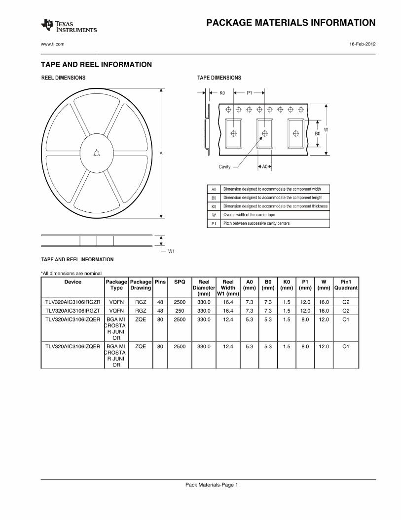
TAPE AND REEL INFORMATION
*All dimensions are nominalDevice Package
TypePackageDrawing
Pins SPQ ReelDiameter(mm)
ReelWidth
W1 (mm)
A0(mm)
B0(mm)
K0(mm)
P1(mm)
W(mm)
Pin1Quadrant
TLV320AIC3106IRGZR VQFN RGZ 48 2500 330.0 16.4 7.3 7.3 1.5 12.0 16.0 Q2TLV320AIC3106IRGZT VQFN RGZ 48 250 330.0 16.4 7.3 7.3 1.5 12.0 16.0 Q2TLV320AIC3106IZQER BGA MI
CROSTAR JUNI
OR
ZQE 80 2500 330.0 12.4 5.3 5.3 1.5 8.0 12.0 Q1
TLV320AIC3106IZQER BGA MI CROSTA
R JUNI OR
ZQE 80 2500 330.0 12.4 5.3 5.3 1.5 8.0 12.0 Q1
PACKAGE MATERIALS INFORMATION
www.ti.com 16-Feb-2012
Pack Materials-Page 1
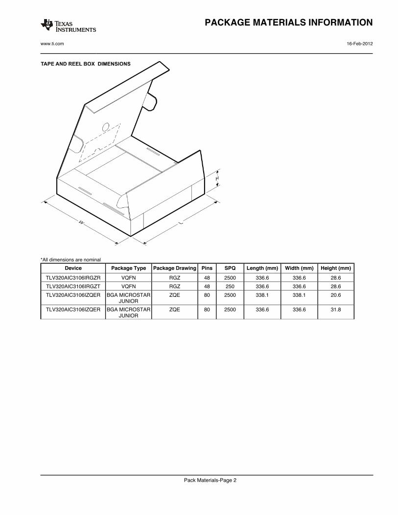
*All dimensions are nominalDevice Package Type Package Drawing Pins SPQ Length (mm) Width (mm) Height (mm)
TLV320AIC3106IRGZR VQFN RGZ 48 2500 336.6 336.6 28.6TLV320AIC3106IRGZT VQFN RGZ 48 250 336.6 336.6 28.6TLV320AIC3106IZQER BGA MICROSTAR
JUNIORZQE 80 2500 338.1 338.1 20.6
TLV320AIC3106IZQER BGA MICROSTARJUNIOR
ZQE 80 2500 336.6 336.6 31.8
PACKAGE MATERIALS INFORMATION
www.ti.com 16-Feb-2012
Pack Materials-Page 2
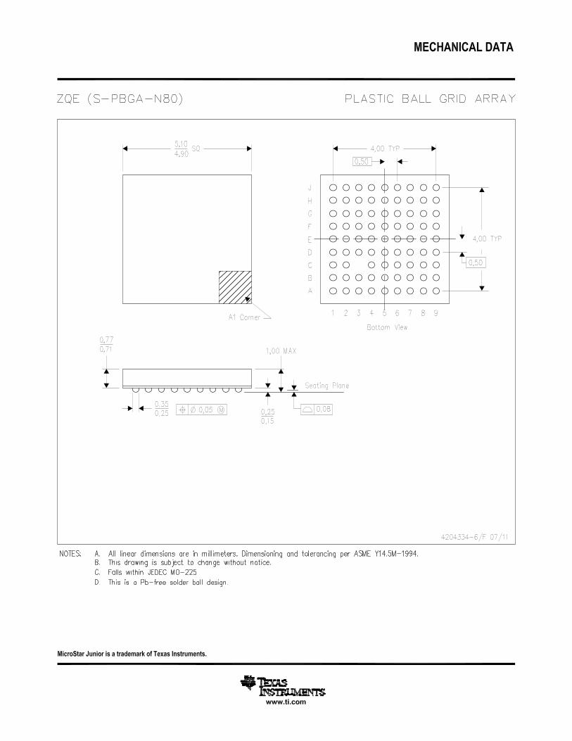

IMPORTANT NOTICETexas Instruments Incorporated and its subsidiaries (TI) reserve the right to make corrections, modifications, enhancements, improvements,and other changes to its products and services at any time and to discontinue any product or service without notice. Customers shouldobtain the latest relevant information before placing orders and should verify that such information is current and complete. All products aresold subject to TI¶s terms and conditions of sale supplied at the time of order acknowledgment.TI warrants performance of its hardware products to the specifications applicable at the time of sale in accordance with TI¶s standardwarranty. Testing and other quality control techniques are used to the extent TI deems necessary to support this warranty. Except wheremandated by government requirements, testing of all parameters of each product is not necessarily performed.TI assumes no liability for applications assistance or customer product design. Customers are responsible for their products andapplications using TI components. To minimize the risks associated with customer products and applications, customers should provideadequate design and operating safeguards.TI does not warrant or represent that any license, either express or implied, is granted under any TI patent right, copyright, mask work right,or other TI intellectual property right relating to any combination, machine, or process in which TI products or services are used. Informationpublished by TI regarding third-party products or services does not constitute a license from TI to use such products or services or awarranty or endorsement thereof. Use of such information may require a license from a third party under the patents or other intellectualproperty of the third party, or a license from TI under the patents or other intellectual property of TI.Reproduction of TI information in TI data books or data sheets is permissible only if reproduction is without alteration and is accompaniedby all associated warranties, conditions, limitations, and notices. Reproduction of this information with alteration is an unfair and deceptivebusiness practice. TI is not responsible or liable for such altered documentation. Information of third parties may be subject to additionalrestrictions.Resale of TI products or services with statements different from or beyond the parameters stated by TI for that product or service voids allexpress and any implied warranties for the associated TI product or service and is an unfair and deceptive business practice. TI is notresponsible or liable for any such statements.TI products are not authorized for use in safety-critical applications (such as life support) where a failure of the TI product would reasonablybe expected to cause severe personal injury or death, unless officers of the parties have executed an agreement specifically governingsuch use. Buyers represent that they have all necessary expertise in the safety and regulatory ramifications of their applications, andacknowledge and agree that they are solely responsible for all legal, regulatory and safety-related requirements concerning their productsand any use of TI products in such safety-critical applications, notwithstanding any applications-related information or support that may beprovided by TI. Further, Buyers must fully indemnify TI and its representatives against any damages arising out of the use of TI products insuch safety-critical applications.TI products are neither designed nor intended for use in military/aerospace applications or environments unless the TI products arespecifically designated by TI as military-grade or �enhanced plastic.� Only products designated by TI as military-grade meet militaryspecifications. Buyers acknowledge and agree that any such use of TI products which TI has not designated as military-grade is solely atthe Buyers risk, and that they are solely responsible for compliance with all legal and regulatory requirements in connection with such use.TI products are neither designed nor intended for use in automotive applications or environments unless the specific TI products aredesignated by TI as compliant with ISO/TS 16949 requirements. Buyers acknowledge and agree that, if they use any non-designatedproducts in automotive applications, TI will not be responsible for any failure to meet such requirements.Following are URLs where you can obtain information on other Texas Instruments products and application solutions:
Products ApplicationsAudio www.ti.com/audio Automotive and Transportation www.ti.com/automotiveAmplifiers amplifier.ti.com Communications and Telecom www.ti.com/communicationsData Converters dataconverter.ti.com Computers and Peripherals www.ti.com/computersDLP� Products www.dlp.com Consumer Electronics www.ti.com/consumer-appsDSP dsp.ti.com Energy and Lighting www.ti.com/energyClocks and Timers www.ti.com/clocks Industrial www.ti.com/industrialInterface interface.ti.com Medical www.ti.com/medicalLogic logic.ti.com Security www.ti.com/securityPower Mgmt power.ti.com Space, Avionics and Defense www.ti.com/space-avionics-defenseMicrocontrollers microcontroller.ti.com Video and Imaging www.ti.com/videoRFID www.ti-rfid.comOMAP Mobile Processors www.ti.com/omapWireless Connectivity www.ti.com/wirelessconnectivity
TI E2E Community Home Page e2e.ti.com
Mailing Address: Texas Instruments, Post Office Box 655303, Dallas, Texas 75265Copyright � 2012, Texas Instruments Incorporated