TI Information – Selective Disclosure 1 Characterizing Bias Current Spikes A wideband...
20
1 TI Information – Selective Disclosure Characterizing Bias Current Spikes A wideband transimpedance amplifier was used to directly view the input current of several chopper amplifiers Wideband TIA Device Under Test Input Curren t
-
Upload
baldwin-brent-stevenson -
Category
Documents
-
view
219 -
download
0
Transcript of TI Information – Selective Disclosure 1 Characterizing Bias Current Spikes A wideband...

1TI Information – Selective Disclosure
Characterizing Bias Current Spikes
A wideband transimpedance amplifier was used to directly view the input current of several chopper amplifiers
Wideband TIA
Device Under Test
Input Current

2TI Information – Selective Disclosure
Characterizing Bias Current Spikes
SpikeUNUNUBUBFOUT IIIIIRV )2()1()2()1(
OPA657 OPA2188
Bias Current (IB) 2 pA 160 pA
Current Noise (IN) 1.3 fA/rtHz 7 fA/rtHz
Bias current spikes should be apparent above other noise sources

3TI Information – Selective Disclosure
Input Bias Spike Measurement Equipment
• A shielded enclosure was used to mitigate extrinsic noise
• Direct connection to the oscilloscope via coax cable
Spikes were viewed on a 500 MHz oscilloscope
– 50 Ohm input impedance
– DC coupling (maximize bandwidth)
– Averaging used to remove random noise

4TI Information – Selective Disclosure
OPA2188• Spikes repeat at 2x the
chopper clock frequency
• Larger spike is due to the input commutation
• Smaller spike is from the synchronous notch filter on the output
• Largest spike peaks at 850nA
• Total duration is ~24nS

5TI Information – Selective Disclosure
OPA2333
Different input topology– Transmission gates reduce
input current spikes
– 70 nA peak
– 216 nS duration
Commutation frequency is much lower
– Input clock spikes are now of similar magnitude to notch filter spikes
6TI Information – Selective Disclosure
AD8639
This is not unique to TI auto-zero topologies!
1.7 uA!

7TI Information – Selective Disclosure
Noise Feed-Through
Without proper design considerations noise from the input current spikes can appear in the output

8TI Information – Selective Disclosure
Equivalent Schematic
Input current spikes can be viewed as current sources on the inputs
Input current spikes are outside the opamp bandwidth– The opamp can be
removed to simplify analysis
– Current spikes on the non-inverting input are not amplified

9TI Information – Selective Disclosure
Contribution to Output Noise
Output noise is dependant upon:– Input current spike magnitude– Feedback network impedance (RF and RG)– Load Impedance (RLOAD)
Current spikes on the inverting input are coupled to the load by the feedback network
)||(21 LOADFGG RRRIV
LOADF
LOADOUT RR
RVV
1

10TI Information – Selective Disclosure
Noise Measurement
RBWKA
VNoise
NV
RMSHzV
)/(
• Output noise was amplified and viewed on a spectrum analyzer– OPA2211 with a gain of 11
– HP3588 (10Hz to 150MHz)• Data collected using LabView
– Shielded enclosure and cables
VRMS: Output voltage
AV: Gain of secondary amplifier
KN: Brickwall correction factor (1.056)
RBW: Resolution Bandwidth

11TI Information – Selective Disclosure
Gain Effects on Total Noise
At high gains chopper noise is not a dominant noise contributor

12TI Information – Selective Disclosure
Load Impedance Effects
High load impedances can exacerbate chopper noise from input current spikes
13TI Information – Selective Disclosure
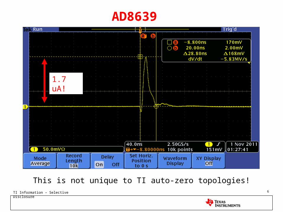
Feedback Network Impedance
Large feedback resistor values will also worsen the output noise
14TI Information – Selective Disclosure
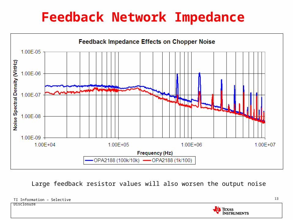
Output Filtering
Adding an RC output filter can mitigate noise seen by high impedance loads
– COUT chosen to have an impedance much less than RLOAD at 2x chopping frequency
– ROUT chosen to maintain opamp stability with the chosen COUT
OUTOUTC CRf
21

15TI Information – Selective Disclosure
Output Filtering
• The corner frequency for the input current spike is actually much lower– The filter now includes the feedback resistance RF
– Filter corner frequency can be chosen to remove noise without affecting desired signal
OUTFOUTSPIKEC CRR
f
)(2
1)(

16TI Information – Selective Disclosure
Output Filtering
kHznFCR
fOUTOUT
C 15910*100*2
1
2
1
kHznFkCRR
fOUTFOUT
SPIKEC 576.110)10100(2
1
)(2
1)(
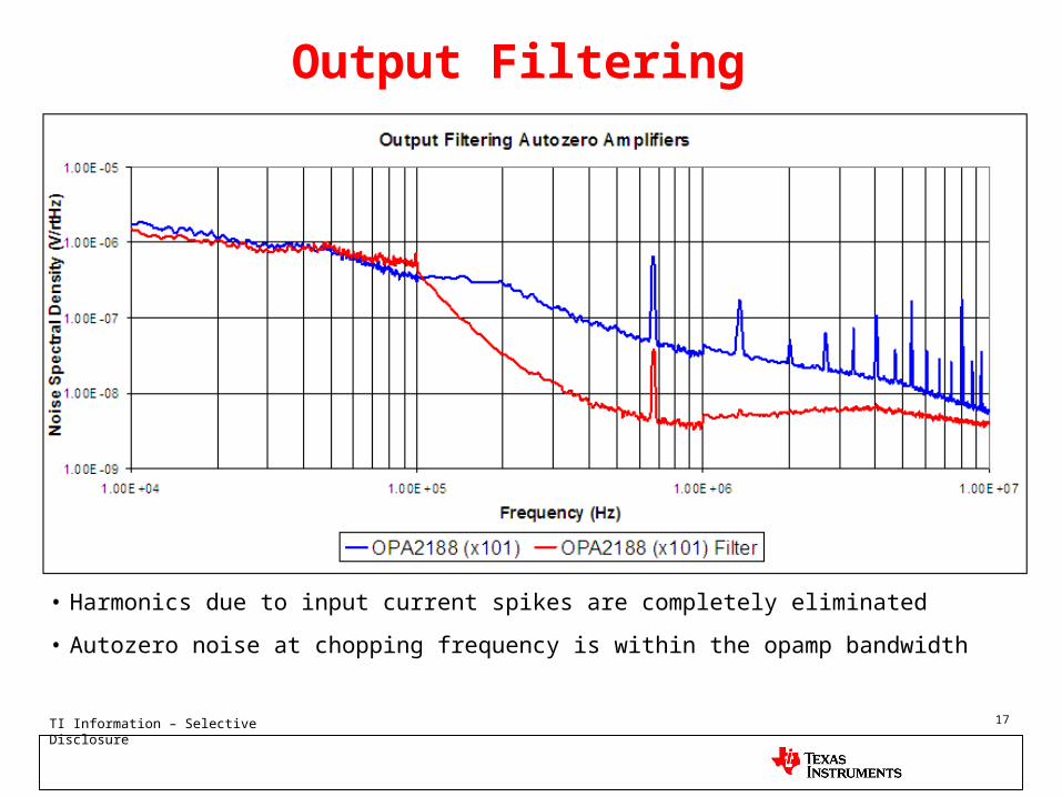
17TI Information – Selective Disclosure
Output Filtering
• Harmonics due to input current spikes are completely eliminated
• Autozero noise at chopping frequency is within the opamp bandwidth

18TI Information – Selective Disclosure
Output Filtering
OPA2188 Without Filtering– Gain: 101, RF:10k, RG:100 Ohm– Oscilloscope 1MOhm input
impedance is the load– Input current spikes are visible
above other noise sources
OPA2188 With Filtering– Gain: 101 RF: 10k, RG: 100 Ohm
– Oscilloscope 1MOhm input impedance is the load
– Triggering oscilloscope becomes difficult due to low noise

19TI Information – Selective Disclosure
Comparison to Non-Autozero Amplifiers
The noise level of a filtered chopper amplifier is on-par with non-chopper topologies

20TI Information – Selective Disclosure
Minimizing Chopper Noise Effects
• Input current spikes are not amplified by the part– Spikes on the inverting input will be coupled to the load by the feedback
network
• Minimize feedback resistance values– Reduces the voltage produced by current spikes
– Standard design practice for low-noise, low-drift circuits
• Load impedance directly contributes to the magnitude of voltage produced by the spike
• An RC filter is an extremely effective way to reduce output noise– Corner frequency can be placed outside of the signal bandwidth
– Noise through the feedback network experiences a much greater attenuation