A Wideband Transimpedance Amplifier - Stanford...
22
A Wideband Transimpedance Amplifier EE 214 Design Project Winter 2010 Azadeh Moini, Milad Mohammadi
-
Upload
truongtuyen -
Category
Documents
-
view
242 -
download
10
Transcript of A Wideband Transimpedance Amplifier - Stanford...

A Wideband Transimpedance Amplifier
EE 214 Design Project
Winter 2010
Azadeh Moini, Milad Mohammadi
!
2!!
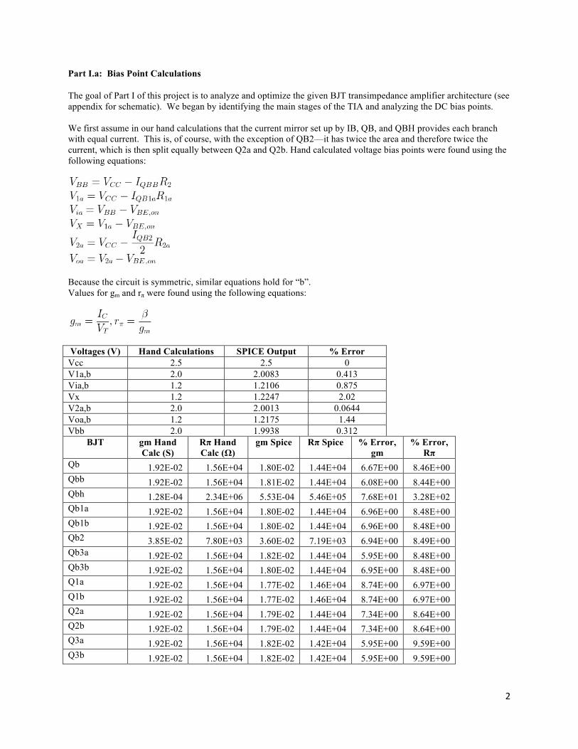
Part I.a: Bias Point Calculations
The goal of Part I of this project is to analyze and optimize the given BJT transimpedance amplifier architecture (see appendix for schematic). We began by identifying the main stages of the TIA and analyzing the DC bias points. We first assume in our hand calculations that the current mirror set up by IB, QB, and QBH provides each branch with equal current. This is, of course, with the exception of QB2—it has twice the area and therefore twice the current, which is then split equally between Q2a and Q2b. Hand calculated voltage bias points were found using the following equations:
Because the circuit is symmetric, similar equations hold for “b”. Values for gm and rπ were found using the following equations:
Voltages (V) Hand Calculations SPICE Output % Error Vcc 2.5 2.5 0 V1a,b 2.0 2.0083 0.413 Via,b 1.2 1.2106 0.875 Vx 1.2 1.2247 2.02 V2a,b 2.0 2.0013 0.0644 Voa,b 1.2 1.2175 1.44 Vbb 2.0 1.9938 0.312
BJT gm Hand Calc (S)
Rπ Hand Calc (Ω)
gm Spice Rπ Spice % Error, gm
% Error, Rπ
Qb 1.92E-02 1.56E+04 1.80E-02 1.44E+04 6.67E+00 8.46E+00 Qbb 1.92E-02 1.56E+04 1.81E-02 1.44E+04 6.08E+00 8.44E+00 Qbh 1.28E-04 2.34E+06 5.53E-04 5.46E+05 7.68E+01 3.28E+02 Qb1a 1.92E-02 1.56E+04 1.80E-02 1.44E+04 6.96E+00 8.48E+00 Qb1b 1.92E-02 1.56E+04 1.80E-02 1.44E+04 6.96E+00 8.48E+00 Qb2 3.85E-02 7.80E+03 3.60E-02 7.19E+03 6.94E+00 8.49E+00 Qb3a 1.92E-02 1.56E+04 1.82E-02 1.44E+04 5.95E+00 8.48E+00 Qb3b 1.92E-02 1.56E+04 1.80E-02 1.44E+04 6.95E+00 8.48E+00 Q1a 1.92E-02 1.56E+04 1.77E-02 1.46E+04 8.74E+00 6.97E+00 Q1b 1.92E-02 1.56E+04 1.77E-02 1.46E+04 8.74E+00 6.97E+00 Q2a 1.92E-02 1.56E+04 1.79E-02 1.44E+04 7.34E+00 8.64E+00 Q2b 1.92E-02 1.56E+04 1.79E-02 1.44E+04 7.34E+00 8.64E+00 Q3a 1.92E-02 1.56E+04 1.82E-02 1.42E+04 5.95E+00 9.59E+00 Q3b 1.92E-02 1.56E+04 1.82E-02 1.42E+04 5.95E+00 9.59E+00

3""
Part I.c: Determining the mid-band loop gain, T0,and transresistance First, we identify that the circuit is a fully differential TIA, and we identify the main stages: Stage 1 is a couple of common base devices (current buffer) that have a current gain of approximately 1. Stage 2 is a voltage-amplifying differential pair. The gain for this stage is given below. Stage 3 is a source follower (voltage buffer) that buffers the output voltage to allow for a larger output voltage swing and a lower output impedance. The gain of this stage is found to be smaller than 1. To calculate the low-frequency gain of the system, we made the following assumptions:
1. The current mirror is not in the signal path and hence is neglected. 2. CBB and Cca are short-circuit in small signal analysis as they are large. For the same reason, Cpa is
open-circuit. 3. The differential pair is symmetric and has a virtual ground at its emitters. 4. In calculating the first stage gain, rπ2is neglected because it is large compared to R1a.
The stage-by-stage gain calculations are as follows:
In the above expressions, a is the forward gain, f is the feedback gain, T0is the loop gain, and A is the closed loop gain.

4""
Part I.d: Determining the Poles of the system To determine the loop gain, T(jω), poles, we first include the loads of the shunt-shunt feedback network into the forward gain path. Once done, we recognize that we have three nodes that produce high frequency poles, namely: Stage1 Input Node, Stage 2 Input Node, and Stage 3 Input Node. To calculate the three dominant poles of the system, we made the following assumptions:
1. Ignore: rµ, rc, re, re,r0, rb 2. Do not assume gain of Stage 3 is 1(gm*R is not large enough to assume this) 3. Make Miller assumption (ignoring zeros) 4. Capacitors in consideration: Cµ, Cπ, Cpa 5. CBB, Cc, Cpcapacitors are short-circuit for small signal analysis 6. Cµ1of the common base stage and Cµ3 of the source-follower stage are grounded on one end and do
not create Miller effect In this design, we "Miller" two capacitors: Cµ of Stage 2 and Cπ of Stage 3, because they are the only two whose input and output are in the signal path. The equivalent input impedance of a load after applying the Miller effect is Z'=Z/(1-K), and the equivalent output impedance is Z'=Z*K/(1-K). Furthermore, Cµ2 acts as a pole splitter. We use the pole splitting equation on slide 31 of lecture 15 to determine the equation for the pole at the input node of stage 3 (input at stage 2 includes the Miller of Cµ2). Note that in order to achieve accurate results, we used the most accurate expression (with no simplifications) from lecture 15to calculate the pole splitting effect.
Here, “p1” is at the input of stage 2, and “p2” is at the input of stage 3. We essentially have 3 nodes, and therefore 3 poles, one at the input of each stage. The hand calculated pole values are computed using the following equations:
and their results are tabulated below: Poles Frequency (GHz) Node
1 1.51 Input of Stage 1 2 1.77 Input of Stage 2 3 48.1 Input of Stage 3

5""
Part I.e: Determining the location of the closed-loop poles from root-locus analysis Below is the Root Locus plot we obtained from MATLAB using the zpk command and the poles calculated in Part I.
The location of the closed loop poles using were found using T0 calculated in Part I.c, T(s) poles calculated in Part I.d, and the equation on slide 43 of Lecture 14:
As shown above, the closed loop poles we find in from our root locus are all in the LHP (negative). Thus, we determine that the amplifier is stable. Based on our root locus plot, the angle of the complex pole with the axis is ~80°. In our MFM lecture, we learned that if the angle with the axis is greater than ~45° or, in some cases, 60°, then we should expect peaking. In our case, therefore, we expect peaking (see page 8 for more details). The angle of the dominant complex conjugate pole is found by finding twice the angle from the ‘negative of the Real axis’ to closed loop poles found above. Each pole has an angle of 78.7° with the axis. Therefore, the total angle between the two complex conjugate poles is 157.45°. Again, this tells us that we should expect peaking in our closed-loop response.
Poles Frequency (GHz) Freq. Mag. (GHz) Node 1 -1.231 + j 6.176 6.2975 Input of Stage 1/2 2 -1.231 –j 6.176 6.2975 Input of Stage 1/2 3 -48.563 48.563 Input of Stage 3
6""
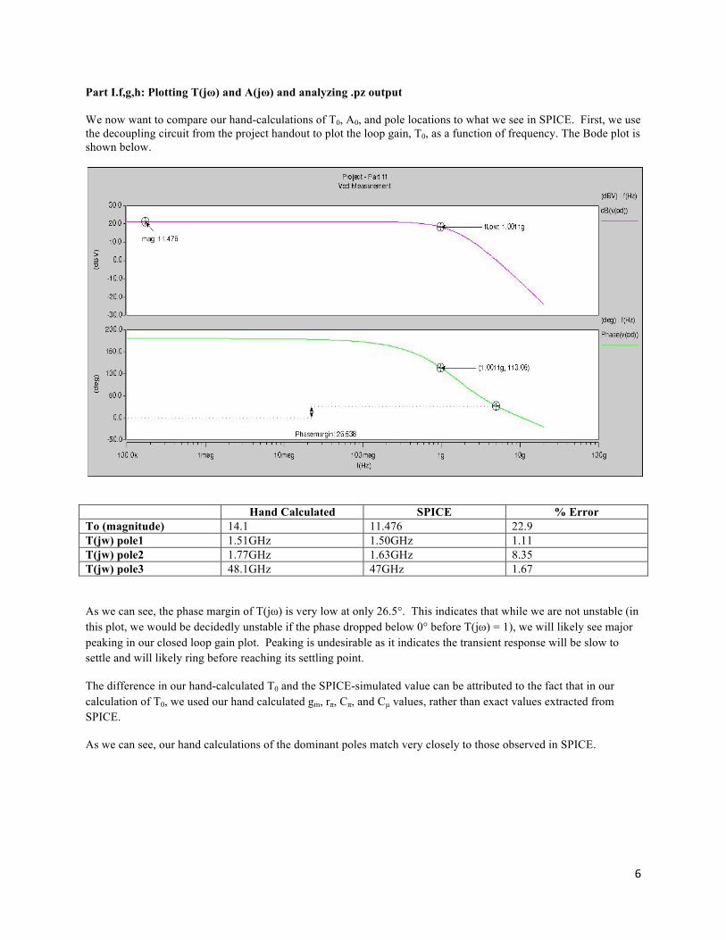
Part I.f,g,h: Plotting T(jω) and A(jω) and analyzing .pz output We now want to compare our hand-calculations of T0, A0, and pole locations to what we see in SPICE. First, we use the decoupling circuit from the project handout to plot the loop gain, T0, as a function of frequency. The Bode plot is shown below.
Hand Calculated SPICE % Error To (magnitude) 14.1 11.476 22.9 T(jw) pole1 1.51GHz 1.50GHz 1.11 T(jw) pole2 1.77GHz 1.63GHz 8.35 T(jw) pole3 48.1GHz 47GHz 1.67
As we can see, the phase margin of T(jω) is very low at only 26.5°. This indicates that while we are not unstable (in this plot, we would be decidedly unstable if the phase dropped below 0° before T(jω) = 1), we will likely see major peaking in our closed loop gain plot. Peaking is undesirable as it indicates the transient response will be slow to settle and will likely ring before reaching its settling point.
The difference in our hand-calculated T0 and the SPICE-simulated value can be attributed to the fact that in our calculation of T0, we used our hand calculated gm, rπ, Cπ, and Cµ values, rather than exact values extracted from SPICE.
As we can see, our hand calculations of the dominant poles match very closely to those observed in SPICE.

7""
We next plot A(jω) in SPICE and look at the outcome. The Bode plot is shown below.
Hand Calculation SPICE % Error Ao (magnitude) 934 919.86 1.52 A(jw) pole1 (1.23+6.18i)GHz = 6.30GHz (1.16+5.34)GHz = 5.46GHz 15.24 A(jw) pole2 (1.23-6.18i)GHz = 6.30GHz (1.16-5.34)GHz = 5.46GHz 15.24 A(jw) pole3 48.6GHz 87.9GHz 44.76
As expected from our phase margin in T(jω), we see huge peaking in A(jω). Our pole calculations for A(jω) came from our root-locus plot. We know that:
"
Therefore, the poles of T(jω) are the poles of A(jω). Our root-locus plot shows how the poles of T(jω) change for different values of T(jω). According to the above equation, we find the poles of A(jω) by solving for T(jω) = -1. As expected, the two low frequency poles are complex but still on the LHP, and the high frequency poles follows the root-locus plot to a higher frequency. The large discrepancy between hand calculations and SPICE calculations for the high frequency pole may somewhat be attributable to the discrepancy in our T0 value.
Total power consumed by this circuit is 10.02mW.

!
8!!
Part I.i: Determining value and effect of adding a feedback (phantom) zero After making the previous plots we notice some peaking in our plot of A(jω). Our goal is to have an overall phase margin in T(jω) of 45° or better (ideally ~60°) to avoid peaking in the closed loop, A(jω), response. We decided we should introduce a feedback, or phantom, zero that will maximize our closed-loop bandwidth without giving us any peaking. The idea is to put a feedback capacitor in parallel with our feedback resistor to introduce a zero in the feedback network. We know that the frequency at which T(jω) = 1 is the 3dB point of A(jω). If we size our feedback capacitor such that our zero is at the frequency where T(jω) = 1, we should be able to achieve 45° phase margin in A(jω). (We know this is true because, according to our pole/zero calculations, we have 2 poles before the -3dB point). To avoid peaking, we will actually want a phase margin of ~60°, so we will start by achieving 45° and pushing the zero to a slightly lower frequency to achieve better phase margin. Our assumptions are as follows: We assume that we can ignore the pole created by our feedback network, as it will be very large and beyond our frequency range of interest. We assume that we will not affect the forward amplifier with our added zero. We further assume that we only have the 3 dominant poles we calculated in previous parts. We find that the frequency at which T(jω) = 1 is 6.30GHz. This makes sense, as it is in fact between the 2nd and 3rd pole we calculated. The frequency of our zero in T(jω) is: 1/(2!"#$#). We set this to 6.30GHz and find Cf = 26fF. After re-plotting our circuit in SPICE with this feedback capacitor included, we find that we get a phase margin of over 61° in T(jω), and in fact, our plot of A(jω) is flat and shows no signs of peaking. This means that our pole did not end up exactly where we predicted. This is reasonable because our hand calculations do not perfectly match the SPICE output, and we made a few assumptions. However, our hand calculations and assumptions must have been reasonable, since we achieve the exact outcome we were hoping for. Our new root locus plot, including our phantom zero, is below. All poles and zeros are always in the LHP, indicating more stability in the circuit, as expected. Additionally, the angle between the negative real axis and our complex poles is now 44.49° according to our MATLAB scripts, meeting the requirements for a flat frequency response.
9""
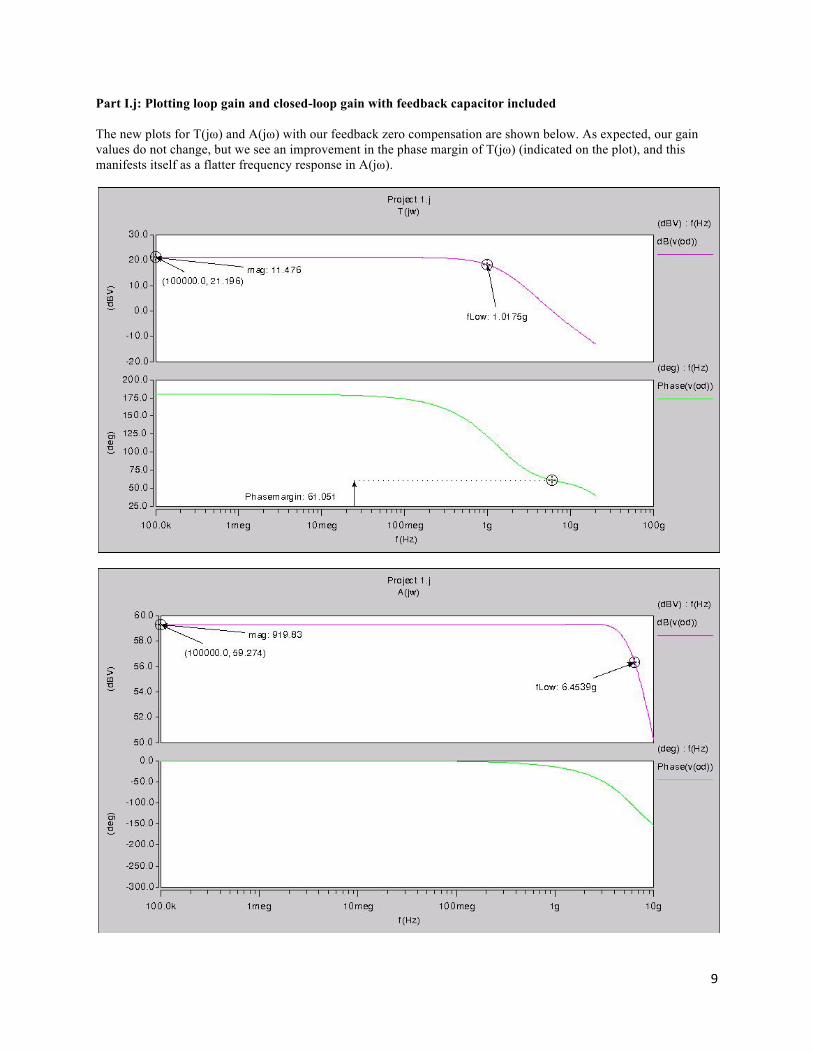
Part I.j: Plotting loop gain and closed-loop gain with feedback capacitor included The new plots for T(jω) and A(jω) with our feedback zero compensation are shown below. As expected, our gain values do not change, but we see an improvement in the phase margin of T(jω) (indicated on the plot), and this manifests itself as a flatter frequency response in A(jω).
10""
We do not expect to see a change in our poles of T(jω), only the addition of a zero. Again, we used our root locus plot to calculate our expected poles for A(jω). Below is a table comparing hand-calculated values and SPICE values for poles of T(jω) and A(jω). *all in GHz Real Imaginary Magnitude
(Hand calc) Real Imaginary Magnitude
(SPICE calc) % Error
T(jω) pole1 1.51 0 1.51 1.46 0 1.46 3.61 T(jω) pole2 1.77 0 1.77 1.64 0 1.64 7.69 T(jω) pole3,4 48.1 0 48.1 34.1 +/- 27.4 43.7 9.35 T(jω) zero1 6.30 0 6.30 6.12 0 6.12 2.94 A(jω) pole1,2 4.87 +/- 4.79 6.83 3.90 +/- 4.56 6 13.83 A(jω) pole3,4 41.3 0 41.3 31.8 +/-24.3 40 3.08
We see reasonable matching between our hand-calculated poles and zeros and those found through SPICE simulations. One interesting note is the high frequency poles we find in both T(jω) and A(jω) are complex, and not real as we calculated. We suspect that the reason for this is that our hand-calculated value of T0 do not perfectly match the value we see in SPICE; therefore, we are on a slightly different location on the root locus map, resulting in the small mismatch we see in our pole calculations.

11""
Part I.k-l: Noise Analysis
To hand calculate the noise, we used the following equations. As shown below, the input referred current noise is dominated by the collector Shot-noise of the common-base stage, Q1, and its corresponding current mirror BJT device, QB1. The subsequent stages contribute negligible amounts to the input referred noise value. Once we realized this, we decided to simplify our analysis by only calculating the main noise sources across the entire circuit. A summary of this work is included below.
The above results match with our noise simulations on SPICE. The PSD input referred current noise we extracted from the plot below is 1.6E-22 A2/Hz which corresponds to 11% error between the simulated and the hand calculated results. We think this mismatch in our values comes from two sources:
1. The approximations we made in calculating the noise (explained above). 2. For hand calculations, we did not include any data from the SPICE simulations. Thus, the diescrepancies
between our hand calculated Ic and Ib values and SPICE values add to the error.
Extra Observation: the input referred voltage noise of this amplifier is approximately the same for all the stages (they are all in the order of 10-19). This is because the resisances of all stages are roughly in the same order of magnitude.
Hand Calc Noise (A2/Hz)
SPICE Noise (A2/Hz)
% Error
1.78E'22" 1.61E'22" 11.1

!
12!!
Part II Design 1: Thoughts, sizing, and biasing In the second part of the project, we will discuss two CMOS-based transimpedance amplifiers (TIA). We decide to begin our CMOS exploration with the same architecture we used in Part I. This is a good way for us to clearly see the differences between our MOSFETs and BJTs. The only change we make in the architecture is to remove the “beta helper” transistor QBH, since MOSFETs draw no gate current. Before we begin, we made a series of predictions. First, β for MOSFETs is infinite. However, it is 300 for the BJTs we use, which here is essentially infinite, indicating that our BJTs are very high performance. From the lecture notes we know that gm/Id is lower for MOSFETs than for BJTs. Therefore, we suspect that if we keep current the same, we will see lower gain in our MOSFET circuit. We note that MOSFETs have no gate noise, whereas BJTs have shot noise at the base. We hope that this will be to our benefit in the noise calculations. Additionally, we think we may be able to use PMOS in some situations if we are hard-pressed to meet the noise specifications, since γ for PMOS is 0.7 and is 0.8 for NMOS. In biasing our CMOS circuit, we have two real knobs: current and gm/Id. Because we predict low gm to be a problem, we start this design by taking the highest current possible (2mA) and a very high gm/Id (18). We realize that a high gm/Id and high Id will give us a large device width, and therefore hurt out bandwidth. Thus, we take the device length to be minimal. Additionally, our initial goal is to meet the gain spec and from there attempt to improve the bandwidth if possible. We only go as high as 18 for gm/Id because our EE214 HSpice noise models become inaccurate beyond this point. However, because we don’t have to worry about distortion, we are still able to use a high gm/Id. Before beginning, we generate two plots for W: one in which we sweep Id for various gm/Id, and one in which we sweep gm/Id for various values of Id. As stated, we decided to go with the largest current and gm/Id, but these plots are included in the appendix and could be useful for increasing bandwidth at the cost of gain if so desired. One thing we notice is that setting all the resistors to zero gives us zero gain, as expected, but drives the bandwidth to 2.28GHz. We think this must be the maximum bandwidth achievable by this circuit. However, as we have a particular gain spec, we continue with our primary goal of reaching this gain. We should note that we begin without the feedback capacitor, as we did in the BJT circuit, and we will later determine if it is necessary. It is valuable to note that Rf, our feedback resistor, does not play a role in DC biasing. However, it plays a crucial role in bandwidth and gain, as later analyses will make clear. Although we start by sizing all our transistors the same, such that each branch receives 2mA of current, we later tweak this a bit. Our gain depends on R1a,b and R2a,b; however, low headroom limits how large these resistors can be sized before pushing other transistors into the linear regime. Therefore, we resize transistors MB1a and MB1b such that our first stage receives half the current as the other stages, allowing us to improve gain to the point of our BJT design. This is described in more detail in the following section. Below is a table with transistor data. Transistor Name Current (A) Width (µm) Length
(µm) gm (S) Cgs (fF) Cgd (fF)
Mb 2.00E-03 319.6 0.18 3.57E-02 433.44 154.35 Mbb 2.08E-03 319.6 0.18 3.69E-02 434.04 154.33 Mb1a 7.13E-04 160 0.18 1.27E-02 215.55 81.14 Mb1b 7.13E-04 160 0.18 1.27E-02 2.16E+02 8.11E+01 Mb2 2.80E-03 640 0.18 4.93E-02 859 325.8 Mb3a 1.58E-03 319.6 0.18 2.90E-02 431.3 156 Mb3b 1.58E-03 319.6 0.18 2.90E-02 431.3 156 M1a 6.50E-04 160 0.18 1.28E-02 204.18 77.36 M1b 6.50E-04 160 0.18 1.28E-02 204.18 77.36 M2a 1.40E-03 319.6 0.18 2.70E-02 412.7 154.47 M2b 1.40E-03 319.6 0.18 2.70E-02 412.7 154.47 M3a 1.64E-03 319.6 0.18 3.09E-02 402.7 154.5 M3b 1.64E-03 319.6 0.18 3.09E-02 402.7 154.5

13##
Part II Design 1: Pole and Gain Analysis We went through a similar process with our CMOS design as with our BJT design in order to fully understand our CMOS design and to gain insight into the differences between these circuits. Here, as in our BJT circuit, we have a fully differential circuit with three stages: a common gate (current buffer), common source, and source follower. First, our pole calculations: we see that our three dominant poles of T(jω) are at the same nodes as our BJT circuit. Our first pole is at the input of stage 1. Our second pole is at the input of stage 2, and our third pole is at the input of stage 3. However, we again have a pole splitting capacitor, Cgd of stage 2. We again make the Miller assumption for both Cgd2 and Cgs3, and assume we can ignore any associated zeros. One big difference we have in CMOS is that we need to take the bulk into account and determine when gmb and Csub are important. In our 1st stage, the common gate, we tie the bulk to ground, not to the source. This gives us 2 bonuses: not only do we short out our dwell cap, but our gm is enhanced by gmb, increasing our gain and bandwidth. In our 2nd stage, the common source, we tie the bulk to the source, which is AC ground. In this stage, we have neither gmb nor Csub. In our 3rd stage, the source follower, we tie the bulk to the source again. We again do not have gmb, but this time we must take Csub into account, since the bulk is not grounded. Csub has a very interesting effect at this node. Because Cgs3 is “Millered”, Csub has the effect of adding a zero at: ! = 1/(2! ∗ !" !" ∗ !"#$ = ~7!"#. This actually falls beyond our 3rd pole so we ignore it. We find that poles 1, 2 and 3 of T(jω): 51.2MHz, 99.6MHz, 4.08GHz. The pole equations are given by the following equations (again, very similar to our BJT analysis):
Next, we calculate the gain stage-by-stage, including ro since it is not significantly larger than our load resistors.

14##
From these gain calculations, it is clear to see why we decreased current in the first stage to increase our gain. Gain in the first stage is dependent only on R1a,b, not on gm. Thus, decreasing gm does not hurt us, and decreasing current allows us to increase R1a and maintain our DC bias points. Additionally, decreasing I decreased our device widths, decreasing the capacitances of our stage 1 transistors, and we see an improvement in the bandwidth. Using these values of T0 and poles, we again make a root locus plot to predict stability and the location of our closed loop poles. Our root locus plot is shown below:
According to the root locus plot, our poles for A(jω) should be on the LHP (values in table below). Since the angle between the negative Real axis and our poles is just at the edge of our requirement for a maximally flat response (59.47°), we will look to the plot (below) to make sure we don’t see peaking. Our next step was to compare our hand calculated values to those actually achieved in SPICE. As seen below in our plot of A(jω), our careful hand analysis paid off. Our gain is the same as our BJT circuit, and, as we expected, we see a flat closed loop response. Our plot of T(jω) also shows a phase margin of 60.6°, again confirming that we should see a flat closed loop response. Note that our closed loop bandwidth has dropped significantly from the BJT case. Again, this is primarily because our large gm/Id and large gm give us large widths, leading to very large capacitances. Furthermore, our flat A(jω) indicates that we do not need a feedback zero in our CMOS case.
15##
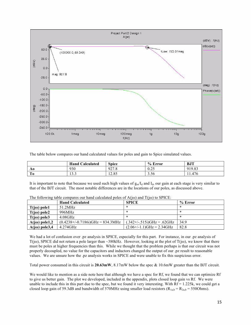
The table below compares our hand calculated values for poles and gain to Spice simulated values. Hand Calculated Spice % Error BJT Ao 930 927.8 0.25 919.83 To 13.3 12.85 3.56 11.476 It is important to note that because we used such high values of gm/Id and Id, our gain at each stage is very similar to that of the BJT circuit. The most notable differences are in the locations of our poles, as discussed above. The following table compares our hand calculated poles of A(jω) and T(jω) to SPICE: Hand Calculated SPICE % Error T(jω) pole1 51.2MHz * * T(jω) pole2 996MHz * * T(jω) pole3 4.08GHz * * A(jω) pole1,2 (0.4238+/-0.7186i)GHz = 834.3MHz (.342+/-.515i)GHz = .62GHz 34.9 A(jω) pole3,4 4.274GHz (2.06+/-1.1)GHz = 2.34GHz 82.8 We had a lot of confusion over .pz analysis in SPICE, especially for this part. For instance, in our .pz analysis of T(jω), SPICE did not return a pole larger than ~380kHz. However, looking at the plot of T(jω), we know that there must be poles at higher frequencies than this. While we thought that the problem perhaps is that our circuit was not properly decoupled, no value for the capacitors and inductors changed the output of our .pz result to reasonable values. We are unsure how the .pz analysis works in SPICE and were unable to fix this suspicious error. Total power consumed in this circuit is 20.63mW, 8.17mW below the spec & 10.6mW greater than the BJT circuit. We would like to mention as a side note here that although we have a spec for Rf, we found that we can optimize Rf to give us better gain. The plot we developed, included in the appendix, plots closed loop gain vs Rf. We were unable to include this in this part due to the spec, but we found it very interesting. With Rf = 1.225k, we could get a closed loop gain of 59.3dB and bandwidth of 570MHz using smaller load resistors (R1a,b = R2a,b = 550Ohms).

!
16!!
Part II Design 1: Noise Analysis To hand calculate the noise, we used the following equations. A summary of our hand analysis of this amplifier is included below.
The above calculations are done using SPICE output data (.op) and approximately match our noise simulations on SPICE. The PSD input referred current noise we extracted from the noise plot below is 1.63E-22 A2/Hz which corresponds to 11.0% error between the simulated and the hand calculated results. We think because the gm/Id=18 in this design is at the onset of the reliability margin of the graph below (obtained from lecture 10), the noise simulations are slightly inaccurate and hence different from what we anticiated. It is very interesting to note that our MOSFET input current noise is very similar to that of our BJT circuit. While we do not have gate leakage current in our CMOS (whereas we have base shot noise in the BJT), we do have a higher γ in CMOS, as well as a slightly higher gm in our design. Additionally, Rf is the same in both circuits. We suspect that these reasons all contribute to our similar noise values.
!
Hand Calc Noise (A2/Hz)
SPICE Noise (A2/Hz)
% Error BJT (A2/Hz)
1.81E'22! 1.63E'22! 11.0 1.61E-22
17##
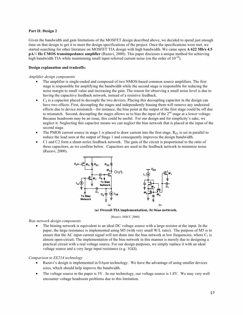
Part II: Design 2 Given the bandwidth and gain limitations of the MOSFET design described above, we decided to spend just enough time on that design to get it to meet the design specifications of the project. Once the specifications were met, we started searching for other literature on MOSFET TIA design with high bandwidth. We came upon A 622 Mb/s 4.5 pA/√ Hz CMOS transimpedance amplifier (Razavi, 2000). This paper discusses a unique method for achieving high bandwidth TIA while maintaining small input referred current noise (on the order of 10-24). Design explanation and tradeoffs: Amplifier design components
• The amplifier is single-ended and composed of two NMOS-based common source amplifiers. The first stage is responsible for amplifying the bandwidth while the second stage is responsible for reducing the noise margin to small value and increasing the gain. The reason for observing a small noise level is due to having the capacitive feedback network, instead of a resistive feedback.
• CS is a capacitor placed to decouple the two devices. Placing this decoupling capacitor in the design can have two effects. First, decoupling the stages and independently biasing them will remove any undesired effects due to device mismatch—for instance, the bias point at the output of the first stage could be off due to mismatch. Second, decoupling the stages allows us to bias the input of the 2nd stage at a lower voltage. Because headroom may be an issue, this could be useful. For our design and for simplicity’s sake, we neglect it. Neglecting this capacitor means we can neglect the bias network that is placed at the input of the second stage.
• The PMOS current source in stage 1 is placed to draw current into the first stage. RD1 is set in parallel to reduce the load seen at the output of Stage 1 and consequently improves the design bandwidth.
• C1 and C2 form a shunt-series feedback network. The gain of the circuit is proportional to the ratio of these capacitors, as we confirm below. Capacitors are used in the feedback network to minimize noise (Razavi, 2000).
[Razavi, ISSCC 2000]
Bias network design components • The biasing network is equivalent to an ideal DC voltage source with a large resistor at the input. In the
paper, the large resistance is implemented using M5 (with very small W/L ratio). The purpose of M5 is to ensure that the AC input current signal will not drain into the bias network at low frequencies, where C1 is almost open-circuit. The implementation of the bias network in this manner is merely due to designing a practical circuit with a real voltage source. For our design purposes, we simply replace it with an ideal voltage source and a very large input resistance (e.g. 1GΩ).
Comparison to EE214 technology
• Razavi’s design is implemented in 0.6µm technology. We have the advantage of using smaller devices sizes, which should help improve the bandwidth.
• The voltage source in the paper is 3V. In our technology, our voltage source is 1.8V. We may very well encounter voltage headroom problems due to this limitation.
18##
Our modifications and calculations:
• In our first design attempt, we tried to design the circuit as shown in the paper. Doing so gave us some insight as to which circuit components are essential for the expected behavior of the design and which ones are there for practicality (Cs, for example). Of course these “practical” circuit components still effect the design performance and need to be optimized. For instance, the sizing of the feedback network is of critical importance. Additionally, if the size of M5 is not chosen wisely, we can observe a zero at 0Hz. We suspect this is due to the AC input current signal being drained into the biasing network rather than in the amplifier (described in more detail below).
• It is important to note that we biased our initial circuit in a similar manner to our previous CMOS design—that is, we take gm/Id to be 18 to attempt to meet the gain spec. Additionally, for simplicity, we sized all the transistors the same (with the exception of M5). Furthermore, we used 2mA in the current sources as a starting point.
• At this point, we did hand analysis for gain and dominant poles. This not only helped us to understand the circuit, but also to choose values for different components. Our hand calculations confirmed that the closed loop transimpedance is in fact proportional to the ratio of the feedback caps, C2/C1. The gain of this design is calculated using the following expressions,
and the three poles of the system are calculated as follows:
• Once we identified the critical design components, we redesigned our circuit to simplify it. Our intention was to first design the ideal circuit and then time permitting, add the rest of the blocks and construct the entire circuit, as described in the paper. However, due to time limitations, we did not manage to include the parts we neglected from the original design.
• The changes we made were as follows. We replaced the PMOS at the first stage with an ideal current source. This, we were hoping, would improve bandwidth by removing any capacitances associated with the PMOS. Additionally, it removes the burden of deciding where to bias the PMOS device. Furthermore, we chose to remove CS, and therefore the 2nd biasing network. Third, we replaced the biasing network with a more simple design using an ideal voltage source and a large input resistor. It is using this biasing network that we see why Razavi emphasized the sizing of M5 in his design. As we mentioned above, if the resistor is too low, the input signal will be redirected to the resistor rather than to the amplifier, and we will get a plot like the one below, rather than a nice flat response.

19##
• Using a large input resistor and the simplified design described above, we observe the following:
Vcc 1.8V RD1 160Ω Iss1 4mA RD2 60Ω Iss2 6mA C1 1.2pF
Length 0.18µm C2 0.1nF Width_stage1 620µm Width_stage2 960µm
Iss1 is the current source that replaces the PMOS. RD1 and RD2 are the load resistors for the 1st and 2nd stages, respectively. Iss2 is the current source that is at the source of the 2nd stage. C1 and C2 form the
20##
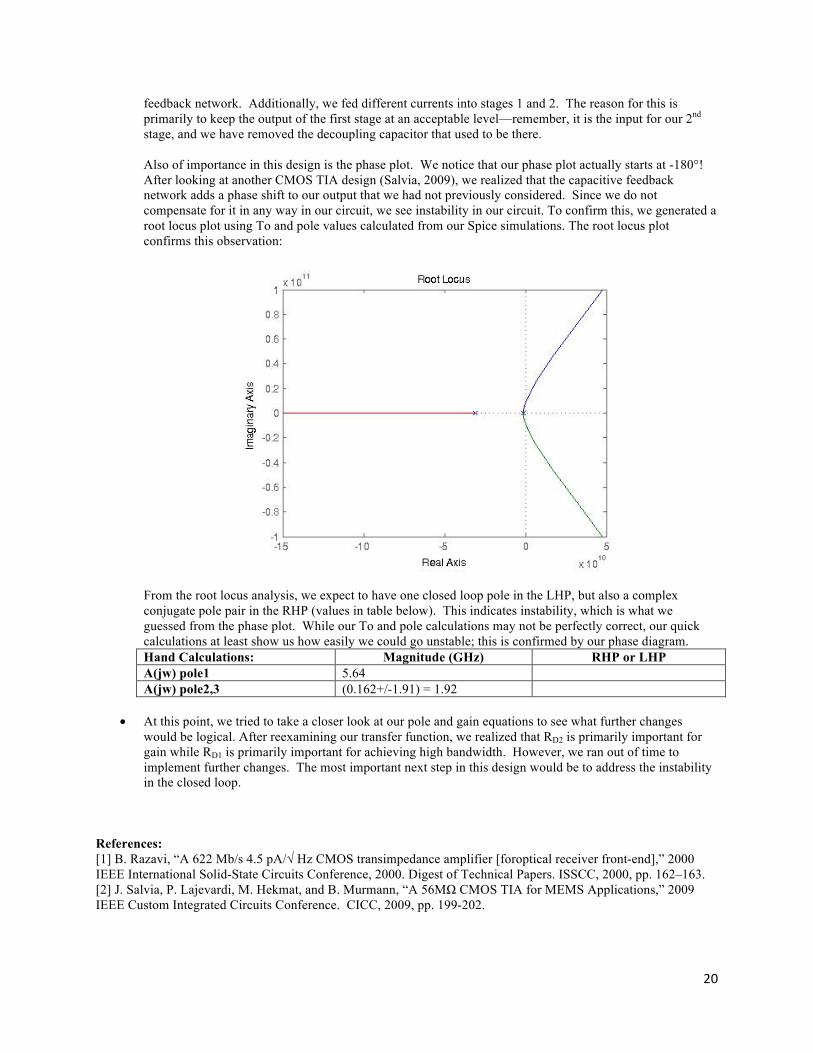
feedback network. Additionally, we fed different currents into stages 1 and 2. The reason for this is primarily to keep the output of the first stage at an acceptable level—remember, it is the input for our 2nd stage, and we have removed the decoupling capacitor that used to be there. Also of importance in this design is the phase plot. We notice that our phase plot actually starts at -180°! After looking at another CMOS TIA design (Salvia, 2009), we realized that the capacitive feedback network adds a phase shift to our output that we had not previously considered. Since we do not compensate for it in any way in our circuit, we see instability in our circuit. To confirm this, we generated a root locus plot using To and pole values calculated from our Spice simulations. The root locus plot confirms this observation:
From the root locus analysis, we expect to have one closed loop pole in the LHP, but also a complex conjugate pole pair in the RHP (values in table below). This indicates instability, which is what we guessed from the phase plot. While our To and pole calculations may not be perfectly correct, our quick calculations at least show us how easily we could go unstable; this is confirmed by our phase diagram. Hand Calculations: Magnitude (GHz) RHP or LHP A(jw) pole1 5.64 A(jw) pole2,3 (0.162+/-1.91) = 1.92
• At this point, we tried to take a closer look at our pole and gain equations to see what further changes would be logical. After reexamining our transfer function, we realized that RD2 is primarily important for gain while RD1 is primarily important for achieving high bandwidth. However, we ran out of time to implement further changes. The most important next step in this design would be to address the instability in the closed loop.
References: [1] B. Razavi, “A 622 Mb/s 4.5 pA/√ Hz CMOS transimpedance amplifier [foroptical receiver front-end],” 2000 IEEE International Solid-State Circuits Conference, 2000. Digest of Technical Papers. ISSCC, 2000, pp. 162–163. [2] J. Salvia, P. Lajevardi, M. Hekmat, and B. Murmann, “A 56MΩ CMOS TIA for MEMS Applications,” 2009 IEEE Custom Integrated Circuits Conference. CICC, 2009, pp. 199-202.

[1] C.F. Liao and S.I. Liu, “40 Gb/s transimpedance-AGC amplifier and CDR circuit for broadband data receivers in 90 nm CMOS,” IEEE Journal of Solid State Circuits, vol. 43, 2008, p. 642.[2] B. Razavi, “A 622 Mb/s 4.5 pA/√ Hz CMOS transimpedance amplifier [foroptical receiver front-end],” 2000 IEEE International Solid-State Circuits Conference, 2000. Digest of Technical Papers. ISSCC, 2000, pp. 162–163.[3] J. Salvia, P. Lajevardi, M. Hekmat, and B. Murmann, “A 56MΩ CMOS TIA for MEMS Applications,” 2009 IEEE Custom Integrated Circuits Conference. CICC, 2009, pp. 199-202.

21##
Appendix BJT Schematic from project handout:
Decoupling schematic: