Recent progress in MOCVD Technology for Electronic and … · 2017-11-20 · Recent progress in...
24
Recent progress in MOCVD Technology for Electronic and Optoelectronic Devices Prof Dr.-Ing. Michael Heuken 1,2 Vice President Corporate Research&Development 1) AIXTRON SE, Dornkaulstr. 2, 52134 Herzogenrath, Germany 2) RWTH-Aachen University, Templergraben 55, 52074 Aachen, Germany AIXTRON SE
Transcript of Recent progress in MOCVD Technology for Electronic and … · 2017-11-20 · Recent progress in...
Recent progress in MOCVD Technology for Electronic and Optoelectronic Devices
Prof Dr.-Ing. Michael Heuken1,2
Vice President Corporate Research&Development
1) AIXTRON SE, Dornkaulstr. 2, 52134 Herzogenrath, Germany2) RWTH-Aachen University, Templergraben 55, 52074 Aachen,
Germany
AIXTRON SE

Contents
Introduction
State of the art MOCVD
Micro LED for Displays
Conclusion and Takeaway
Energy saving by using GaN/AlGaN HEMT

The revolution in mobile telephony
3

Compound semiconductor for power control
4
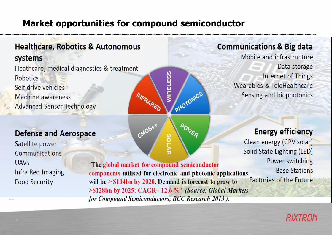
Market opportunities for compound semiconductor
5

Principle of MOVPE
Ga(CH3)3 + AsH3 → GaAs +3CH4
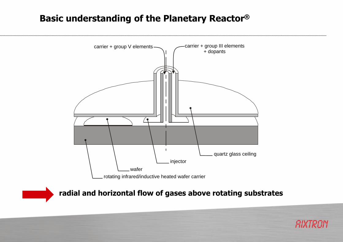
carrier + group III elements+ dopants
carrier + group V elements
wafer
injector
quartz glass ceiling
rotating infrared/inductive heated wafer carrier
Basic understanding of the Planetary Reactor®
radial and horizontal flow of gases above rotating substrates

Gas transport mechanisms in the Planetary Reactor
• Depletion of group-III species results in flat growth rate profile by disc rotation
• Uniformity controlled by balance of convective and diffusive fluxes M.Heuken et al. JCG 303 (2007) 318
8
Resulting growth profile
Distance from center
on rotated waferMOYDJ diff
MOYUJ convect
J = MO species mass flux
= gas density
U = local flow velocity
YMO = mass fraction of MO
D = diffusion coefficient
Dominant species fluxes:
diffusion flux
forced convection flux (by main flow)
Group III
Group V
Group V
Triple injector

NO COMPROMISE IN TUNING:
•Individual wafer rotation and GFR flow control = good on-wafer uniformity by design
•Injector enabling full tuning flexibility
ADVANCED YIELD MANAGEMENT:
•Reset of reactor each run with Cl2 in-situ cleaning No Part Exchange
Excellent Run-to-Run Stability
•Temperature matching between each individual wafers, within a run and run to run
G5+: “Single Wafer performance w Batch reactor cost benefits”
9
Single wafer rotation, combined with radial horizontal gas flow
G5+ 5x200 mm

10
Requirements for MOCVD in HVM:
Cassette-to-Cassette 150/200 mm Si wafer automation for fab integrationand throughput
In-situ Reactor Cleaning for process robustness and yield
On-wafer temperature process control for highest reproducibility and yield
High throughput for lowest Cost-of-ownership (COO)
Qualified device level layer processesfor fast time to market
Cassette-to-Cassette Module
G5+ C Cassette-to-Cassettedual module cluster
Vacuum Robot
AIX G5+ C: CS High-Volume Manufacturing Award 2016

Power Transistor: 100x SL + Active Layers
AIXTRON G5+ C PLANETARY REACTOR® 11
• 100x SL buffer to target 650 V
• Increased carbon level in SL by means of autodoping
• Reference D-Mode device stack with active layers
Bow X (µm) Bow Y (µm)
Sample C 64 44
No strain relaxation even with 100x SL
RT bow comparable to 50x SL
Total thickness: ~5.0 µm
Reflectivity
Curvature
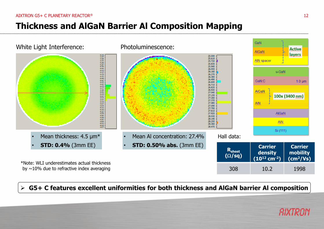
Thickness and AlGaN Barrier Al Composition Mapping
AIXTRON G5+ C PLANETARY REACTOR® 12
• Mean thickness: 4.5 µm*
• STD: 0.4% (3mm EE)
• Mean Al concentration: 27.4%
• STD: 0.50% abs. (3mm EE)
G5+ C features excellent uniformities for both thickness and AlGaN barrier Al composition
*Note: WLI underestimates actual thickness by ~10% due to refractive index averaging
Rsheet
(W/sq)
Carrier density
(1012 cm-2)
Carrier mobility(cm2/Vs)
308 10.2 1998
Hall data:
White Light Interference: Photoluminescence:

I-V Breakdown Characteristics
AIXTRON G5+ C PLANETARY REACTOR® 13
0 250 500 750 1000 1250 150010
-12
10-11
10-10
10-9
10-8
10-7
10-6
10-5
10-4
10-3
10-2
10-1
100
Forward
Reverse
Cu
rre
nt
(A/m
m2)
Voltage (V)
T = 25 °C
0 250 500 750 1000 1250 150010
-12
10-11
10-10
10-9
10-8
10-7
10-6
10-5
10-4
10-3
10-2
10-1
100
Forward
Reverse
Cu
rre
nt
(A/m
m2)
Voltage (V)
T = 150 °C
800 V / 900 V 600 V / 770 V
650 V specification met at room temperature / very close at 150 °C
1 µA/mm2
0 2 4 6 8 10 120
100
200
300
400
I d (
mA
/mm
)
Vds (V)
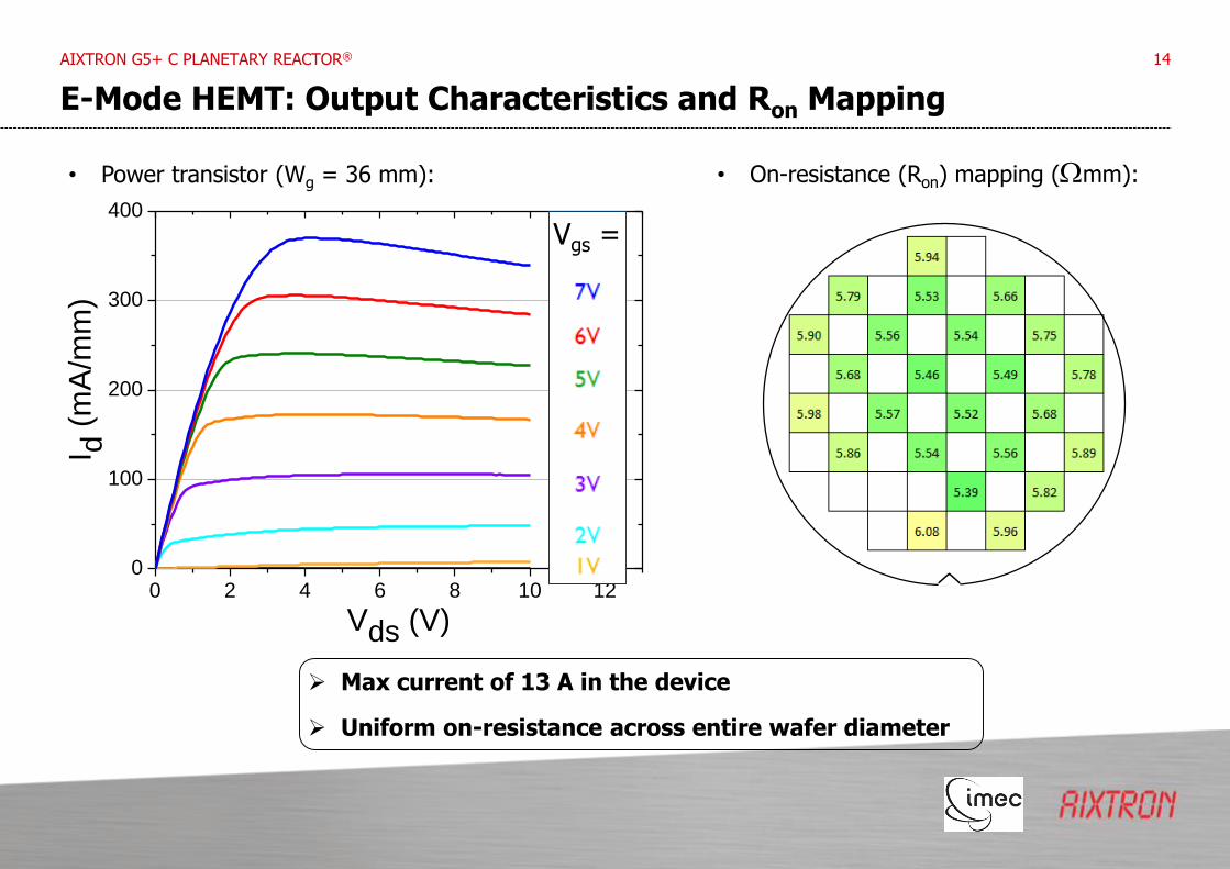
E-Mode HEMT: Output Characteristics and Ron Mapping
AIXTRON G5+ C PLANETARY REACTOR® 14
• Power transistor (Wg = 36 mm):
Max current of 13 A in the device
Uniform on-resistance across entire wafer diameter
• On-resistance (Ron) mapping (Wmm):
Vgs =

Intra & Inter wafer layer thickness uniformity & reproducibility
15
Intra-wafer uniformity: σ/mean=0.44%
Inter-run uniformity: σ/mean=0.24%
Inherent process reproducibility delivers highest on-wafer performance at high throughput!
Mean Thicknessin µm
Inter-Run Intra & Inter-Wafer

16
Sources: Texas Instruments, Electronic Products
Selected products – market penetration

Micro LED and it’s potential as emerging display technologyMicro LED opens a new field of opportunities
Large Size Displays
Smart Watches Augmented Reality
TV Display
Smartphone time
Brightness-> Small pixels-> High contrast ratio
Brightness Efficiency-> battery lifetime
Brightness-> compete with ambient light
-> Color Gamut-> Interactive
Brightness-> battery lifetime-> pixels much smaller than pitch allow integration of sensor matrix
Head Up Display-> High Dynamic Range-> High Definition

Larger Wafer Sizes Required for Micro LED Processing
4“ wafer
52 stamps 10mm x 10mm
3mm E.E.
Fill Factor = 75%
6“ wafer
137 stamps 10mm x 10mm
3mm E.E.
Fill Factor = 84%
Assume: 10mm x 10mm Stamps with Pixels for Transfer
• Larger wafer sizes improve wafer utilization• 6” or 8” Requirement driven by Back End Technology Shift
Courtesy: CALY Technologies

Individual Wafer Temperature Control
• Satelite Wafer Temperature measured by a UV Pyrometer
• Gas foil rotation is individually controlled for each satellite (wafer).
• Flying height of satellite over the main disc determines the temperature adjusted by individual flow rate.
Flying Height Temperature
Topside
Temperature
Measurement
Individual
Flow for each
Satellite (Wafer)
Pyro
MFC MFC
MFC M
FC
MFC

PL Wavelength Uniformity Results for Blue LED
2nm
W/W ~ 0.40nmR/R ~ 0.30nm
on-W
0.55nm
DOM = 450.9nm = 0.50nm(3mm e.e.)
BLUEmLED
InGaN /GaN MQW on sapphire in 8x6“ configuration

PL Wavelength Uniformity Results for Green LED
1.7nm
W/W ~ 0.30nmR/R ~ 0.20nm
on-W ~ 0.75nm
InGaN /GaN MQW on sapphire in 8x6“ configuration
GREENmLED
DOM = 525.9nm = 0.60nm(3mm e.e.)

DOM = 627.0nm
= 0.32nm (3mm e.e.)
1.5nm
W/W ~ 0.30nmR/R ~ 0.25nm
on-W
0.40nm
GaInP /AlGaInP MQW on GaAs in 8x6“ configuration
PL Wavelength Uniformity Results for Red LED
REDmLED

Summary & Key Take Aways
23
AIXTRON is developing a complete CVD manufacturing solution forcompound semiconductor based on existing production technology
GaN based Transistors for Power and Microwave Applications
R/G/B Micro LED production technology for future Displays
Business target: Next Generation MOCVD for HVM

If you have any further questions or require more information, please contact us at: Professor Dr. M. HeukenAIXTRON SEDornkaulstr. 252134 HerzogenrathGermanyPhone +49 (2407) 9030-0Fax +49 (2407) 9030-40E-Mai [email protected]
Thank you very much for your attention.