The PN J 1 4 P-N Junction and Application
10
The P N J UNCTION 17 ◆ In the P type semiconductor there are a large no of majority charge carrier hole and small no of minority charge carrier electron. Similarly, in N type semiconductor there are a large no of majority charge carrier electron and a small no of minority charge carrier holes. But they are electronically neutral and such a piece of extrinsic material is not of practical use. A pure block of intrinsic semiconductor can be so doped by a special manufacturing process that one half of it becomes P type and the other part with becomes N type to produce P-N junction diode that are the building block of all electronic gadgets we use today. After completing this section, we should be able to ❑ Describe how a p-n junction is formed • Discuss diffusion across a p-n junction • Explain the formation of the depletion region • Define barrier potential and discuss its significance ❑ Working principle of p-n junction under forward and reverse bias • Half wave and Bridge rectifier 1–4 P-N Junction and Application If a piece of intrinsic silicon is doped so that part is n-type and the other part is p-type, a p-n junction forms at the boundary between the two regions and a diode is created, as indicated in Figure 1–20(a). The p region has many holes (majority carriers) from the impurity atoms and only a few thermally generated free electrons (minority carriers). The n region has many free electrons (majority carriers) from the impurity atoms and only a few thermally generated holes (minority carriers). p-n junction Depletion region (a) The basic silicon structure at the instant of junction formation showing only the majority and minority carriers. Free electrons in the n region near the p-n junction begin to defuse across the junction and fall into holes near the junction in the p region. Besides this, there are negatively charged Acceptor atom in P region and positively charged Donor atom in the N region. ▲ FIGURE 1–20 (b) Every electron that defuses across the junction combines with a hole to make it neutral in the p region of the junction. As a result, there are only negatively charged Acceptor atom in the p region and positively charged Donor atom left in the n region at the vicinity of the junction that produce electric potential across it. This potential repels the charge carriers to defuse further. This part of the junction region consists of blue arrows showing in Figure 1-20(b), is called depletion region and the electric field produced across it is called barrier potential. Formation of the depletion region. The width of the depletion region is exaggerated for illustration purposes. p region n region – + – + – + – + – + – + – + – + Barrier potential p region n region
Transcript of The PN J 1 4 P-N Junction and Application

The PN JUN CTI ON 17 ◆
In the P type semiconductor there are a large no of majority charge carrier hole and small no of minority charge carrier
electron. Similarly, in N type semiconductor there are a large no of majority charge carrier electron and a small no of
minority charge carrier holes. But they are electronically neutral and such a piece of extrinsic material is not of practical
use. A pure block of intrinsic semiconductor can be so doped by a special manufacturing process that one half of it
becomes P type and the other part with becomes N type to produce P-N junction diode that are the building block of all
electronic gadgets we use today.
After completing this section, we should be able to
❑ Describe how a p-n junction is formed
• Discuss diffusion across a p-n junction
• Explain the formation of the depletion region
• Define barrier potential and discuss its significance ❑ Working principle of p-n junction under forward and reverse bias
• Half wave and Bridge rectifier
1–4 P-N Junction and Application
If a piece of intrinsic silicon is doped so that part is n-type and the other part is p-type, a p-n junction forms at the
boundary between the two regions and a diode is created, as indicated in Figure 1–20(a). The p region has many holes
(majority carriers) from the impurity atoms and only a few thermally generated free electrons (minority carriers). The n
region has many free electrons (majority carriers) from the impurity atoms and only a few thermally generated holes
(minority carriers).
p-n junction Depletion region
(a) The basic silicon structure at the instant of
junction formation showing only the majority
and minority carriers. Free electrons in the n
region near the p-n junction begin to defuse
across the junction and fall into holes near the
junction in the p region. Besides this, there are
negatively charged Acceptor atom in P region
and positively charged Donor atom in the N
region.
▲ FIGURE 1–20
(b) Every electron that defuses across the junction
combines with a hole to make it neutral in the p
region of the junction. As a result, there are only
negatively charged Acceptor atom in the p region
and positively charged Donor atom left in the n
region at the vicinity of the junction that produce
electric potential across it. This potential repels the
charge carriers to defuse further. This part of the
junction region consists of blue arrows showing in
Figure 1-20(b), is called depletion region and the
electric field produced across it is called barrier
potential.
Formation of the depletion region. The width of the depletion region is exaggerated for illustration purposes.
p region n region
– +
– +
– +
– +
– +
– +
– +
– +
Barrier potential
p region n region

2 INTRODUCTION to SEMICONDUCTORS ◆
Formation of the depletion Region
Free electrons in the n region are randomly drifting in all directions. At
the instant of the p-n junction formation, those electrons near the junction
in the n region begin to diffuse across the junction into the p region where
they combine with holes, as shown in Figure 1–20(b).
Electron defuses across the boundary of the p and n region and
combines with a hole to make it neutral in the p region of the junction. So
the n region loses some electrons and the p region loses some holes near
the junction. As a result, a layer of n region at the vicinity of the interface
contains only a no of positively charged pentavalent donor ions that
creates positive potential. Similarly, the layer of p region near the
junction consists of only a no of negatively charged trivalent acceptor
ions producing negative positive potential. These two layers of positive
and negative immovable ions form electric field across it, form depletion
region, as shown in Figure 1–19(b). The term depletion refers to the fact
that this region near the p-n junction is depleted of charge carriers
(electrons and holes) due to diffusion across the junction. This electric
field that opposes the diffusion of charge carriers further, is called barrier
potential or potential barrier. Keep in mind that the depletion region is
formed very quickly and is very thin ( of the order of 10-6 m) compared to
the n region and p region.
Barrier Potential
In the depletion region there are many positive ions in n region and many
negative ions in p region of the pn junction. The forces between the
opposite ions form an electric field, as illustrated in Figure 1–20(b) by the
blue arrows. This electric field offers a barrier to the freely movable
electrons in the n region defuse further. The potential difference across the
depletion region is called the barrier potential and is expressed in volts.
Therefore, external electric potential across the depletion region
equal to the barrier potential with the proper polarity must be applied to
provide energy to the electrons to move across the barrier. But on the
other hand, it is noticed that the internal electric field enables the
minority carriers (electrons in p region and holes in n regions) to flow
across the junction. Thus a very small drift current flows in the reverse
direction.
The barrier potential of a p-n junction depends on several factors,
including the type of semiconductive material, the amount of doping, and
the temperature. The typical barrier potential is approximately 0.7 V for
silicon and 0.3 V for germanium at 258C.
After invention of the electric light
bulb, Edison continued to
experiment and in 1883 found that
he could detect electrons flowing
through the vacuum from the lighted
filament to a metal plate mounted
inside the bulb. This discovery became
known as the Edison effect.
An English physicist, John
Fleming, took up where, Edison left
off and found that the Edison effect
could also, be used to detect radio
waves and convert them to electrical
signals. He went on to develop a two-
element vacuum tube called the
Fleming valve, later known as the
diode. It was a device that allowed
current in only one direction. Modern
p-n junction devices are an outgrowth
of this.
H I S T O R Y N O T E
Russell Ohl, working at Bell Labs in
1940, stumbled on the semiconductor pn
junction. Ohl was working with a silicon
sample that had an accidental crack
down its middle. He was using an
ohmmeter to test the electrical
resistance of the sample when he noted
that when the sample was exposed to
light, the current between the two sides
of the crack made a significant jump.
This discovery was fundamental to the
work of the team that invented the
transistor in 1947.
H I S T O R Y N O T E

SUM MAR Y 19 ◆
Energy Energy
Conduction
band
Valence
band
Minority carriers
Majority carriers
Majority carriers
Minority carriers
Conduction
band
Valence
band
0 p region pn junction n region
0 p region pn junction
and depletion
region
n region
(a) At the instant of junction formation
▲ FIGURE 1–21
(b) At equilibrium
Energy diagrams illustrating the formation of the pn junction and depletion region.
Energy diagrams of the P-N Junction and depletion Region
The valence and conduction bands in an n-type material are at slightly lower
energy levels than the valence and conduction bands in a p-type material.
Recall that p-type material has trivalent impurities and n-type material has
pentavalent impurities. The trivalent impurities exert lower forces on the
outer-shell electrons than the pentavalent impurities. The lower forces in p-
type materials mean that the electron orbits are slightly larger and hence, have
greater energy than the electron orbits in the n-type materials.
An energy diagram for a p-n junction at the instant of formation is shown
in Figure 1–20(a). As we can see, the energy level of the valence and
conduction bands in the n region are slightly, lower than those in the p region,
but, there is a significant amount of overlapping.
The free electrons in the n region that occupy the upper part of the
conduction band in terms of their energy can easily, diffuse across the
junction (they do not have to gain additional energy) and temporarily,
become free electrons in the lower part of the conduction band of p-region.
After crossing the junction, the electrons quickly, lose some energy and fall
into the holes in the valence band of the p-region as indicated in Figure
1–21(a).
At the time of formation of depletion region, the energy level of the
conduction band of the n-region decreases due to the loss of the higher-
energy electrons diffused across the junction. Soon, diffusion ceases as, there
are no electrons left with enough energy to get across the boundary to the
conduction band of the p-region, as indicated by the alignment of the top of
the conduction band of n-region and the bottom of the p-region conduction
band in Figure 1–20(b). At this point, the junction is at equilibrium; and the
formation of depletion region is complete. There is an energy gradient across
the depletion region, which acts as an “energy hill” that an n-region electron
must climb to get to the p region.
20 INTRODUCTION to SEMICONDUCTORS ◆
Biasing of P-N Junction Diode
P-N junction semiconductor crystals is widely used in electronic devices
and serve as a semiconductor counter part of vacuum tube diode which
became obsolete after invention of it. So, it is also named P-N junction
diode. It is basically a p-n with metallic contacts at its ends for the
application of external potential difference. The symbolic representation
of p-n junction diode is shown in figure 1-22. The p end and n are called
Anode and Cathode respectively. The black ring at one end of a diode
indicates the cathode. Now let us see, how it can be connected with the
external potential on the basis of which it is of two types--
a) Forward bias and b) Reverse bias
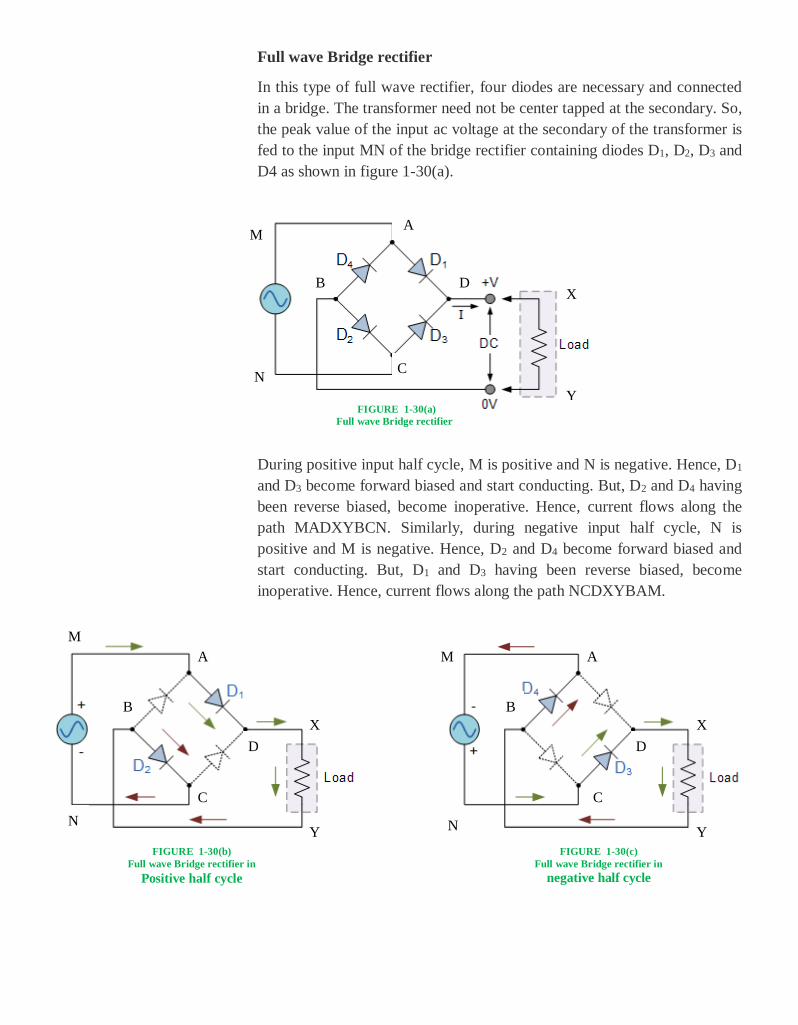
Forward Bias
When the positive terminal and the negative terminal of an external
potential source is connected with p and n region respectively this type
of connection is called forward bias. Hence, it is opposite to the internal
field i.e barrier potential. In this connection, the net potential against the
depletion layer will be reduced that produces negative potential against
the junction as long as the external potential is less than the barrier
potential. In this situation, the charge carriers do not have enough energy
to get through the depletion layer.
Now, if the external potential increases so that, the net potential
against the junction becomes positive, the depletion layer will be
virtually abolished. In this situation, it is possible for the net positive
potential to push the majority charge carriers i.e free electrons and the
holes towards the interface and they cross the barrier.
After diffusion through the depletion layer, electrons recombine
with the holes in the p region and reduce the concentration of the holes
in the p region. At that time, same no of electrons enter the positive
terminal of the external potential from the electron-hole pair of the
covalent bond that produce hole to maintain the previous concentration
of the hole in p region. Similarly, positive holes defuse the depletion
layer to recombine with the electrons in the n region that reduce the
concentration of the electrons. To compensate it, electrons enter the n
region from the negative terminal of the external source. Thus a
continuous current I flows in the conventional direction (from p to n) as
shown in figure 1-23.
The drift current produced by the minority carriers, however,
remain unchanged and small, because the rate of formation of electron-
hole pair is independent of the electric field, unless it is very large.
▲ FIGURE 1–22
Symbol of P-N junction Diode
▲ FIGURE 1–23

Forward Bias Characteristics
If the external potential increases from zero the net potential against
depletion layer increases from negative net potential and no forward current
will flow as shown in figure 1-24. But, when external positive potential
exceeds (the barrier potential 0.3 V for Ge and 0.7 V for Si, 1.2V for
GaAs), the barrier becomes virtually, abolished as net potential becomes
zero. This potential is called knee potential or threshold or offset voltage.
After that, by supplying greater external voltage to produce positive
net voltage, the electrons get enough energy to overcome the potential
barrier (depletion layer) and cross the junction. The same thing happens
with the holes as well. In this situation, the junction becomes forward
biased and forward current increases with the increases of external
potential. Then, the diode current flows rapidly with very small increase of
voltage which follows nonlinear curve as shown in figure 1-24. This is
forward characteristics of p-n diode. In this non-linear region the dynamic
resistance can be defined as, IV
dR .
Reverse Bias
When the positive terminal and the negative terminal of an external
potential source is connected with n and p region respectively, this type of
connection is called reverse bias as shown in figure 1-25. In this situation,
the net potential against the diode corresponds to the more negative
potential. The width of the depletion layer will virtually be wider and the
majority charge carriers (electron in n and hole in p region) do not have
enough energy to get through the depletion layer.
The drift current carried by the minority carriers (electron in p and
hole in n region) however, is not affected. Electrons in p and hole in n
region can flow in the direction of the field from n to p. But, the number of
minority carriers being very small, the drift current is very small (of the
order of microampere) compared to current under forward bias.
FIGURE 1-24
FIGURE-1-25
Reverse Bias

20 INTRODUCTION to SEMICONDUCTORS ◆ Therefore, the conduction current is contributed by the majority charge carrier in forward bias but by
the minority carrier in the reverse bias. The situation is entirely different in a conductor. In a conductor, only
free electrons take part in electric current nor the holes. Therefore, the same current can flow in the opposite
direction, when the voltage is reversed.
Therefore, it can be concluded that, p-n diode acts like a valve, which opens only in one direction.
Current can flow through the p-n diode only in the direction from p to n under forward bias and practically,
no current flows in opposite direction under reverse bias condition.
Reverse Bias characteristics
The direction of reverse bias potential and barrier potential are same and
along n side to p side. Therefore, if the bias potential increases from zero,
the net potential against the junction increases. The layer becomes,
virtually, wider that opposes the flow of majority charge carriers. In this
situation, very feeble current of the order of μA flows due to the flow of
minority charge carriers (electrons in p and holes in n region) in the reverse
direction as shown in figure 1-26. This current remains constant with the
increase of reverse voltage. This current is called reverse saturation
current.
As the reverse bias potential increases, the majority carrier, electrons
of the n region and holes of p region, are attracted respectively, towards
positive terminal and negative terminal of the external potential. Therefore,
majority carrier start accumulating at the opposite ends of the diode, as a
result, the deletion width at the surface of separation becomes extended to a
large extent. In this situation, both electrons and holes are bound together
with Coulomb attraction.
But, a large no of electron-hole pair will be produced when a certain
large reverse voltage is applied. Huge no of electrons will be released
through the n side end due to the large attraction by the positive terminal.
Similarly, same no of electrons will enter the p region from the negative
terminal and recombine with the hole that results huge reverse current. It
seems that electron flows from p to n region that results abruptly high
current along reverse direction. This phenomenon is called Reverse Break
down (Avalanche and Zener break down) held at breakdown voltage and in
this situation, diode gets destroyed.
FIGURE-1-26
Reverse Bias Characteristic

Diode as rectifier
Rectification means conversion of alternating voltage (or current) to direct
voltage. An n-p diode can be used as a rectifier. There are two types of
Rectifier----a) Half wave rectifier, and b) Full wave rectifier
Half wave rectifier
From the previous explanation, it is clear that diode operates in forward
bias and it remains inoperative in reverse bias condition. The necessary
circuit diagram of half wave rectifier is given below in figure-1-27(b).
The alternating voltage to be rectified is applied across the primary of
a suitable transformer and the secondary of the transformer is connected to
the p-n junction diode D through a load resistance RL. The output is
obtained across RL with alternative interruption.
Explanation
The transformer converts the alternating voltage of the source to the
required voltage in the secondary. The secondary provides alternating
potential to the diode D. The wave form of the input is represented by the
figure 1-27(a). Therefore, the diode D gets positive and negative potential
alternatively. During positive half cycle, the diode is forward biased and
conducts electricity. This current flows through the load resistance RL from
top to bottom and returns back to the secondary winding of the transformer.
But during negative half cycle, being reverse biased the diode don’t
conduct current. So, one directional interrupted output current flows
through the load RL from X to Y only, during alternate half-cycle. The
output wave form is shown in figure 1-27(c).
The dc value of the output is the same as the average value which is
0318.00 VVV
dc
, where V0 =peak value of the input
voltage. Thus the average dc value of the output is 31.85 of peak value.
FIGURE-1-27(a) FIGURE-1-27(b) FIGURE-1-27(c)
Input Waveform Circuit Diagram of Halfwave Rectifier Output Waveform
X
Y

20 INTRODUCTION to SEMICONDUCTORS ◆
Full wave rectifier
If we like to get a rectified voltage during both the half cycles of an input
AC voltage, we require a full wave rectifier in which output power is
receive uninterruptedly against load resistance RL. This type of rectifier is
called full wave rectifier. It is of two types—
i) Center tapped full wave rectifier
ii) Full wave Bridge rectifier
Center tapped full wave rectifier
The alternative voltage source is connected at the input primary of a
transformer and the secondary is connected with two p-n junction diodes
D1 and D2 as shown in figure 1-28. Then, the center tapped point and the
common point of the two diodes are joined with a load resistance against
which unidirectional uninterrupted output voltage can be received as shown
in figure 1-28.
Explanation
The alternating voltage at P1 and P2 with respect to the central tap point are
out of phase (phase difference = π) with each other. Therefore, during
positive half-cycle, diode D1 is forward biased and conducts current
through load resistance RLoad from top to bottom indicated by orange arrow
in the figure 1-28 while the other diode D2 is inoperative having been
reverse biased.
Similarly, during negative half cycle, diode D2 is forward biased and
conducts current through the load resistance RLoad along same direction
indicated by green arrow while the other diode D1 is inoperative having
been reverse biased.
Therefore, D1 and D2 operate alternatively and so, a unidirectional
uninterrupted current can be achieved against the load for both the cycles
of the input voltage. The output wave form is shown in figure 1-29.
FIGURE 1-28
FIGURE 1-29
Full wave Bridge rectifier
In this type of full wave rectifier, four diodes are necessary and connected
in a bridge. The transformer need not be center tapped at the secondary. So,
the peak value of the input ac voltage at the secondary of the transformer is
fed to the input MN of the bridge rectifier containing diodes D1, D2, D3 and
D4 as shown in figure 1-30(a).
During positive input half cycle, M is positive and N is negative. Hence, D1
and D3 become forward biased and start conducting. But, D2 and D4 having
been reverse biased, become inoperative. Hence, current flows along the
path MADXYBCN. Similarly, during negative input half cycle, N is
positive and M is negative. Hence, D2 and D4 become forward biased and
start conducting. But, D1 and D3 having been reverse biased, become
inoperative. Hence, current flows along the path NCDXYBAM.
FIGURE 1-30(b)
Full wave Bridge rectifier in
Positive half cycle
FIGURE 1-30(a)
Full wave Bridge rectifier
FIGURE 1-30(c)
Full wave Bridge rectifier in
negative half cycle
M
N
N
M
C
A
B
Y
D X
D
B
C
A
X
Y
M
N
B
D
C
X
Y
A

20 INTRODUCTION to SEMICONDUCTORS ◆
Therefore, current flows through the load from X to Y during both
cycle of the input voltage and unidirectional uninterrupted output voltage
can be received at the output. The output wave form corresponding to the
input potential is shown in figure 1-31.
Difference between Center tapped and Bridge rectifier
Center Tapped Rectifier Bridge Rectifier
Description
Center tapped rectifier as the name suggest is
requires a center tapped transformer (secondary
winding).
No center tapped transformer is required in bridged rectifier.
Peak Inverse
Voltage
The peak inverse voltage (PIV) of diode in center
tapped full wave rectifier is twice the transformer secondary terminal voltage.
Peak inverse voltage PIV of diode is equal to the
transformer secondary voltage. Thus this type of rectifier can be used for high voltage application.
Number Of
Diodes
Center tapped rectifier uses only two diodes in its circuit.
Bridge rectifier uses four diodes in its circuit. This
result to increment in the circuit complexity in case
of the bridge rectifier.
Transformer
Utilization
Factor
(TUF)
The transformer utilization factor (TUF) is equal to 0.672
The transformer utilization factor (TUF) is equal to 0.810 for bridge rectifier.
Voltage
Drop Across
Voltage drop across the two diodes of center
tapped rectifier is less when compared to bridge rectifier.
The voltage drop across the 4 diodes of bridge
rectifier is more than the voltage drop across center tapped rectifier.
Size Of
Transformer
(kVA rating)
The transformer required in center tapped rectifier
is bigger.
The transformer required in bridge rectifier is smaller than that required in center tapped rectifier
in terms of kVA rating.
Economic
Efficiency
Center tapped transformer is economically
efficient since it uses only two diodes in its circuit.
Bridge rectifier is economically inefficient since it
uses four diodes in its circuit.
FIGURE 1-31
Input Waveform
Output waveform for full
cycle
Check up 1. What is a p-n junction?
2. Explain diffusion.
3. Describe the depletion region.
4. Explain what the barrier potential is and how it is created.
5. What is the typical value of the barrier potential for a silicon diode?