Televisión y Videograbadora Especificaciones generales ...
68
MV9KD1 Televisión y Videograbadora Especificaciones generales Instrucciones de desensamble Clave para abreviaturas Lista de modos de servicio Revisiones preventivas e intervalos de servicio Nota para el reemplazo del IC de memoria Jigs de servicio y herramientas Preparación para el servicio Ajustes mecánicos Ajustes eléctricos Diagramas a bloques Placas de circuitos impresos Diagrama esquemático Formas de onda Vistas explotadas mecánicas Vistas explotadas del chasis (para ver) Lista de partes de reemplazo mecánicas Lista de partes de reemplazo del chasis Lista de partes de reemplazo eléctricas
Transcript of Televisión y Videograbadora Especificaciones generales ...
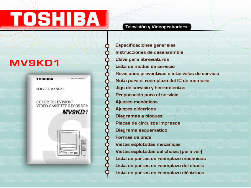
MV9KD1
Televisión y Videograbadora
Especificaciones generales
Instrucciones de desensamble
Clave para abreviaturas
Lista de modos de servicio
Revisiones preventivas e intervalos de servicio
Nota para el reemplazo del IC de memoria
Jigs de servicio y herramientas
Preparación para el servicio
Ajustes mecánicos
Ajustes eléctricos
Diagramas a bloques
Placas de circuitos impresos
Diagrama esquemático
Formas de onda
Vistas explotadas mecánicas
Vistas explotadas del chasis (para ver)
Lista de partes de reemplazo mecánicas
Lista de partes de reemplazo del chasis
Lista de partes de reemplazo eléctricas

SERVICE MANUAL
COLOR TELEVISION/VIDEO CASSETTE RECORDER
FILE NO. 140-200015
MV9KD1

SERVICING NOTICES ON CHECKING
6. AVOID AN X-RAY1. KEEP THE NOTICES
As for the places which need special attentions,they are indicated with the labels or seals on thecabinet, chassis and parts. Make sure to keep theindications and notices in the operation manual.
3. USE THE DESIGNATED PARTS
5. TAKE CARE TO DEAL WITH THECATHODE-RAY TUBE
In the condition that an explosion-proof cathode-ray tube is set in this equipment, safety issecured against implosion. However, whenremoving it or serving from backward, it isdangerous to give a shock. Take enough care todeal with it.
Safety is secured against an X-ray by consider-ing about the cathode-ray tube and the highvoltage peripheral circuit, etc.Therefore, when repairing the high voltage pe-ripheral circuit, use the designated parts andmake sure not modify the circuit.Repairing except indicates causes rising of highvoltage, and it emits an X-ray from the cathode-ray tube.
Please include the following informations when you order parts. (Particularly the VERSION LETTER.)1. MODEL NUMBER and VERSION LETTER
The MODEL NUMBER can be found on the back of each product and the VERSION LETTER can be found at the end of the SERIAL NUMBER.2. PART NO. and DESCRIPTION
You can find it in your SERVICE MANUAL.
HOW TO ORDER PARTS
PERFORM A SAFETY CHECK AFTERSERVICING
7.
Confirm that the screws, parts and wiring whichwere removed in order to service are put in theoriginal positions, or whether there are theportions which are deteriorated around theserviced places serviced or not. Check theinsulation between the antenna terminal orexternal metal and the AC cord plug blades.And be sure the safety of that.
(INSULATION CHECK PROCEDURE)
1.2.
3.
4.
Unplug the plug from the AC outlet.Remove the antenna terminal on TV and turnon the TV.Insulation resistance between the cord plugterminals and the eternal exposure metal[Note 2] should be more than 1M ohm byusing the 500V insulation resistance meter[Note 1].If the insulation resistance is less than 1Mohm, the inspection repair should berequired.
[Note 1]
If you have not the 500V insulationresistance meter, use a Tester.
[Note 2]External exposure metal: Antenna terminal
Earphone jack
2. AVOID AN ELECTRIC SHOCKThere is a high voltage part inside. Avoid anelectric shock while the electric current isflowing.
The parts in this equipment have the specificcharacters of incombustibility and withstandvoltage for safety. Therefore, the part which isreplaced should be used the part which hasthe same character.Especially as to the important parts for safetywhich is indicated in the circuit diagram or thetable of parts as a mark, the designatedparts must be used.
4. PUT PARTS AND WIRES IN THEORIGINAL POSITION AFTERASSEMBLING OR WIRINGThere are parts which use the insulationmaterial such as a tube or tape for safety, orwhich are assembled in the condition thatthese do not contact with the printed board.The inside wiring is designed not to get closerto the pyrogenic parts and high voltage parts.Therefore, put these parts in the originalpositions.

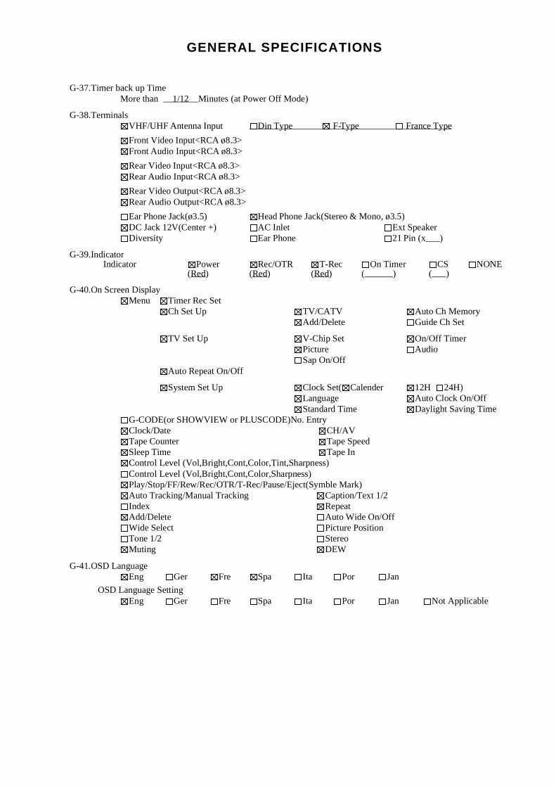
GENERAL SPECIFICATIONS
G-1.Outline of the Product 9 inch(222.8mmV):Measured diagonallyColor CRT 90 degree deflection 2 -Speed 1/2" Video Cassette Recorder
VHS Recorder/PlayerVHS-C Player
G-2.VCR FormatVHS Standard NTSC PAL SECAM PAL-M PAL-N
VHS Hi-Fi Audio System
G-3.Video Recording System :Rotary,slant azimuth two head helical scan systemLuminance Component :FM recordingChrominance Component :Low frequency converted direct recording
G-4.Broadcasting System US System M
G-5.Color System NTSC PAL SECAM or Monochrome signal
G-6.NTSC Playback(PAL 60Hz) Yes No Not Applicable
G-7.MESECAM Yes No Not Applicable
G-8.Cassette TapeVHS type video cassette tape Width 12.65mm (1/2 Inch)VHS-C type video cassette tape Width 12.65mm (1/2 Inch)
G-9.Tape SpeedNTSC or PAL-M PAL or SECAM
SP 33.35 mm/sec SP 23.39 mm/secLP 16.67 mm/sec LP 11.69 mm/secSLP(EP) 11.12 mm/sec
G-10.Recording/Playback TimeNTSC or PAL-M
at SP Mode Max. 210 min. (with T-210 cassette)at LP Mode Max. 420 min. (with T-210 cassette)at SLP(EP) Mode Max. 630 min. (with T-210 cassette)
PAL or SECAMat SP Mode Max. 300 min. (with E-300 cassette)at LP Mode Max. 600 min. (with E-300 cassette)
G-11.DeckOVD-5 OVD-6 OVD-6S
G-12.Rewind/Fast Forward Time(Approx.) FF:1'48" / Rew:1'48" (with T-120 cassette) (with E-180 cassette)
G-13.Search SpeedSP 3 and 5 TimesLP TimesSLP(EP) 9 and 15 Times
G-14.Slow SpeedSP TimesLP TimesSLP(EP) Times
G-15.Frame AdvanceSP TimesLP TimesSLP(EP) Times

GENERAL SPECIFICATIONS
G-16.Antenna Input ImpedanceVHF/UHF 75 ohm unbalanced
G-17.Tuner and Receiving channel 1Tuner System 2Tuner System BS Tuner
Tuner : Contactless Electric tuner
Oscar(W/O HYPER) Oscar(W/ HYPER) France CATV) Otherschannel coverage
2 ~ 69 , 4A , A-5 ~ A-1 , A ~ I , J ~ W , W+1 ~ W+84Tuning System
Frequency syn. Voltage syn. Others
G-18.Preset Channel: -- channels
G-19.Intermediate FrequencyPicture(FP) 45.75 MHz MHz MHzSound (FS) 41.25 MHz MHz MHzFP-FS 4.50 MHz MHz MHz
G-20. Stereo/Dual TV SoundYes( NICAM GERMAN USA JAPAN JAPAN BS) No
G-21.Video SignalInput Level 1 Vp-p / 75 ohmOutput Level 1 Vp-p / 75 ohmS/N Ratio 50 dB (Weighted)Horizontal Resolution at SP Mode 220 Lines
G-22.Audio SignalInput Level
Line - dB / - KohmRCA - 8 dB / 50 Kohm
Output LevelLine - dB / - KohmRCA - 8 dB / 1 Kohm
(0dB=0.775 V rms)
S/N Ratio at SP Mode 38 dBHarmonic Distortion : 1.5 % (1KHz)
Frequency Response : at SP Mode 100 Hz ~ 10 KHzat LP Mode Hz ~ KHzat SLP(EP) Mode 100 Hz ~ 4 KHz
Hi-Fi Model’s Spes NONEDepth Multiplex Recording Rotary, Slant Azimuth Two HeadSystem Helical Scan SystemDynamic Range : More than -- dBWow And Flutter : Less than --- % WrmsChannel Separation : More than -- dBHarmonic Distortion : Less than -- %
G-23.HeadsVideo 2 Rotary Heads Track Width(SP/LP/SLP : 1ch 26 µm, 2ch 31 µm)FM Audio Rotary Heads Track Width(SP/LP/SLP : 1ch µm, 2ch µm)Audio / Control 1 Stationary Head ( Mono Stereo(L,R) )Erase 1 Full Track Erase
G-24.Motor: 3 MotorsTape/Cassette LoadingCylinder (Direct Drive)Capstan (Direct Drive)
G-25.Power Source 120 V AC 50Hz AC 60Hz
EXT DC Jack 12 V

GENERAL SPECIFICATIONS
G-26.Power Consumption: 54 W at AC 120 V 60 Hz 48 W at DC 12 V (at TV and VCR ON)
Stand by: 5 W at AC 120 V 60 HzPer Year: -- kWh / Year
G-27.Dimensions(Approx.) 278 mm(W) 306.5 mm(D) 311.5 mm(H)
G-28.Weight(Approx.) Net : 8.8 Kg ( 19.4 lbs)Gross: 10.5 Kg ( 23.1 lbs)
G-29.Cabinet MaterialCabinet Front: PS 94HB DECABROM
ABS 94V2 NON-DECA94V0
Cabinet Rear: PS 94HB DECABROMABS 94V2 NON-DECA
94V0Jack Panel: PS 94HB DECABROM
ABS 94V2 NON-DECA94V0
G-30.Cassette Loading System: Front Cassette Loading System Top Loading System
G-31.Tape Counter: Linear Time Tape Counter
G-32.Protector: Power Fuse Dew Sensor
G-33.RegulationSafety
UL CSA SAA SI CE SEVBS NF NEMKO FEMKO DEMKO IEC65SEMKO NZ HOMOLO SABS CNS SISIRNOM AS3159 DENTORI UNE GOST NONE
RadiationFCC DOC FTZ PTT CE SEVSABA SI NF NZ HOMOLO UNECNS CISPR13 DENTORI AS/NZS NONE
X-RadiationDHHS HWC PTB DENTORI NONE
G-34.TemperatureOperation 5 ºC ~ 40 ºCStorage -20 ºC ~ 60 ºC
G-35.Operating Humidity Less than 80 %RH
G-36.Clockand TimerCalender : 1990/1/1 ~ 2081/12/31 (Initial 2000/1/1 2005/1/1)Built-in 1 Month 8 Events Programmable TimerOne Touch Recording : Max Time 5 HoursSleep Timer Yes Max 120 Min.( 10 Min. Step) NoOn/Off Timer Yes 1 Programs NoWake Up Timer Yes Programs NoAuto Shut Off 15 Minutes
GENERAL SPECIFICATIONS
G-37.Timer back up TimeMore than 1/12 Minutes (at Power Off Mode)
G-38.TerminalsVHF/UHF Antenna Input Din Type F-Type France Type
Front Video Input<RCA ø8.3>Front Audio Input<RCA ø8.3>
Rear Video Input<RCA ø8.3>Rear Audio Input<RCA ø8.3>
Rear Video Output<RCA ø8.3>Rear Audio Output<RCA ø8.3>
Ear Phone Jack(ø3.5) Head Phone Jack(Stereo & Mono, ø3.5)DC Jack 12V(Center +) AC Inlet Ext SpeakerDiversity Ear Phone 21 Pin (x )
G-39.IndicatorIndicator Power Rec/OTR T-Rec On Timer CS NONE
(Red) (Red) (Red) ( ) ( )
G-40.On Screen DisplayMenu Timer Rec Set
Ch Set Up TV/CATV Auto Ch MemoryAdd/Delete Guide Ch Set
TV Set Up V-Chip Set On/Off TimerPicture AudioSap On/Off
Auto Repeat On/Off
System Set Up Clock Set( Calender 12H 24H)Language Auto Clock On/OffStandard Time Daylight Saving Time
G-CODE(or SHOWVIEW or PLUSCODE)No. EntryClock/Date CH/AVTape Counter Tape SpeedSleep Time Tape InControl Level (Vol,Bright,Cont,Color,Tint,Sharpness)Control Level (Vol,Bright,Cont,Color,Sharpness)Play/Stop/FF/Rew/Rec/OTR/T-Rec/Pause/Eject(Symble Mark)Auto Tracking/Manual Tracking Caption/Text 1/2Index RepeatAdd/Delete Auto Wide On/OffWide Select Picture PositionTone 1/2 StereoMuting DEW
G-41.OSD LanguageEng Ger Fre Spa Ita Por Jan
OSD Language SettingEng Ger Fre Spa Ita Por Jan Not Applicable

GENERAL SPECIFICATIONS
G-42.SpeakerPosition Front Side BottomSize 3 inchesImp. 8 ohm x 1 pcsOutput Max 1.2 W
10% 0.8 W (Typical)
G-43.EXT SpeakerYes W Imp ohm No
G-44.CartonMaster Carton: Need No Need
Content: ---- SetMaterial: ---- / ---- Corrugated CartonDimensions: ---- mm(W) ---- mm(D) ---- mm(H)Description of Origin Yes No
Gift BoxMaterial Double/Brown Corrugated Carton ( with Photo Label)
Double/White Corrugated Carton ( with Photo Label)Double Full Color Carton W/Photo
Dimensions: 338 mm(W) 376 mm(D) 386 mm(H)Design: As Per BUYER 'sDescription of Origin: Yes No
Drop Test Natural Dropping At 1 Corner / 3 Edges / 6 SurfacesHeight 25cm 31cm 46cm 62cm 80cm
Container Stuffing: 1,256 Sets / 40' container
G-45.AccessoriesChannel Film Dew/AHC Caution SheetOwner's Manual ( W/Guarantee Card) [English]Remote Control Unit AC Plug AdaptorRod Antenna ( One Pole Two Pole/ F-Type DIN Type France Type)Loop Antenna( F-Type DIN Type France Type)U/V Mixer Quick Set-up SheetDC Car Cord (Center+) Battery (UM- 4 x 2 )Guarantee Card AC CordWarning Sheet AV Cord (2Pin-1Pin)Circuit Diagram Registration CardAntenna Change Plug PTB SheetService Facility List 300 ohm to 75 ohm Antenna AdaptorImportant Safeguard Euro Warranty Information SheetESP Card
G-46.Other FeaturesAuto Head CleaningAuto Tracking Auto SearchAuto ClockVIDEO PLUS+(SHOWVIEW,G-CODE)HQ (VHS Standard High Quality)Auto Power On, Auto Play, Auto Rewind, Auto EjectForward / Reverse Picture Search SQPBAuto CH Memory CATVClosed Caption CM Skip(30sec x 6Times)TV Auto Shutt off Function Energy StarV-chip( USA CANADA)TV Monitor

GENERAL SPECIFICATIONS
G-47.SwitchFront Power Channel Up Volume Up
Play Channel Down Volume DownPause/Still F.FWD/Cue Rew/RevSystem Select Eject/Stop Rec/OTROne Touch Playback Main Power SW Input Select
Rear Color On/Off (SECAM only) DegaussMain Power SW AC/DC
G-48.Magnetic FieldBV : +0.45G BV : +0.35G BV : +0.25GBH : 0.18G BH : 0.30G BH : 0.30GBV : -0.15G BV : -0.25G BV : -0.50GBH : 0.15G BH : 0.15G BH : 0.30G
G-49.Remote Control Unit:Unit: RC-DQFormat : NEC Custom Code : 40-BF/44-BB hGlow in Dark Remocon Yes NoPower Source: D.C 3 V Battery UM - 4 x 2Total 42 Keys
0 Power Tracking Auto 1 Rec/OTR(2Key) Tracking Up/Set + 2 Play Tracking Down/Set - 3 F.Fwd Menu 4 Rew Enter 5 Pause/Still Cancel 6 Stop Muting 7 Eject Volume Up 8 Timer Rec(2Key) Volume Down 9 TV/Caption/Text Ch UpSleep Timer Ch DownQuick View Zero Return Input Select
Counter Reset SpeedCall CM Skip(Skip Search) Audio Select(for Hi-Fi)Slow(for 4Head) Program( /VCR PLUS+) VCR PLUS+

Main PCB3
1
Main PCB Holder
VCR Block
DISASSEMBLY INSTRUCTIONS
1. REMOVAL OF MECHANICAL PARTSAND P.C. BOARDS
1-1: BACK CABINET (Refer to Fig. 1-1)
1.2.3.
4.
Remove the 4 screws 1.Remove the 2 screws 2.Remove the 2 screws 3 which are used for holding theBack Cabinet.Remove the Back Cabinet in the direction of arrow.
1-3: TV/VCR BLOCK (Refer to Fig. 1-3)
1.2.
3.
Remove the 2 screws 1.Disconnect the following connectors:(CP353, CP401 and CP403).Remove the TV/VCR Block in the direction of arrow.
Front Cabinet
TV/VCR Block
1 1
Fig. 1-3
1-4: MAIN PCB (Refer to Fig. 1-4)
1.
2.3.4.5.6.
Disconnect the following connectors:(CP502, CP820 and CP501).Remove the screw 1.Remove the Main PCB Holder.Remove the 2 screws 2.Remove the screw 3.Remove the Main PCB in the direction of arrow.
Fig. 1-4
2
2
Fig. 1-1
Front Cabinet
Back Cabinet
1
3
1
1-2: CRT PCB (Refer to Fig. 1-2)
CAUTION: BEFORE REMOVING THE ANODE CAP,DISCHARGE ELECTRICITY BECAUSE ITCONTAINS HIGH VOLTAGE.BEFORE ATTEMPTING TO REMOVE ORREPAIR ANY PCB, UNPLUG THE POWERCORD FROM THE AC SOURCE.
1.
2.
3.
Remove the Anode Cap.(Refer to REMOVAL OF ANODE CAP)Disconnect the following connectors:(CP801 and CP850).Remove the CRT PCB in the direction of arrow.
1
1
2
2
3
Front Cabinet CRT PCB
Fig. 1-2

2
1
1
Deck Shield Plate
VCR Block
DISASSEMBLY INSTRUCTIONS
1-5: DECK SHIELD PLATE (Refer to Fig. 1-5)
1.2.3.
Remove the 2 screws 1.Remove the screw 2.Remove the Deck Shield Plate in the direction of arrow.
1-7: JACK PLATE AND SYSCON PCB (Refer to Fig. 1-7)
1.2.3.4.5.6.7.
Remove the screw 1.Remove the Syscon PCB in the direction of arrow (A).Remove the 2 screws 2.Remove the nut 3.Remove the washer 4.Unlock the 2 supports 5.Remove the Jack Plate in the direction of arrow (B).
Jack Plate
1
Deck Holder
Syscon PCB
(A)
5
5
(B)
Fig. 1-7
22
4
3
Fig. 1-5
1-6: DECK CHASSIS (Refer to Fig. 1-6)
1.2.
3.
Remove the 3 screws 1.Disconnect the following connectors:(CP1001, CP1002, CP1004, CP1005, CP1006, CP4001,CP4002 and CP4003).Remove the Deck Chassis in the direction of arrow.
Deck Chassis
Syscon PCB
Fig. 1-6
11
1

DISASSEMBLY INSTRUCTIONS
2. REMOVAL OF DECK PARTS2-1: TOP BRACKET (Refer to Fig. 2-1)
Remove the 2 screws 1.Slide the 2 supports 2 and remove the Top Bracket.
1.2.
NOTE
When you install the Top Bracket, install the screw (1)first, then install the screw (2).
1(2)
Top BracketTop Bracket
Main Chassis
Main Chassis
2
1(1)
2
Fig. 2-1
NOTE
When you install the Tape Guide L, install as shown in thecircle of Fig. 2-3-B. (Refer to Fig. 2-3-B)
REC Lever
Tape Guide L
• The REC Lever is not installed on the Video Cassette Player. Fig. 2-3-B
2-4: CASSETTE HOLDER ASS'Y (Refer to Fig. 2-4)
Move the Cassette Holder Ass'y to the front side.Push the Locker R to remove the Cassette Side R.Remove the Cassette Side L.
1.2.3.
Main Chassis
Main ChassisCassette Side L
Cassette Side R
Fig. 2-4
2-5: CASSETTE SIDE L/R (Refer to Fig. 2-5)
Unlock the 4 supports 1 and then remove the CassetteSide L/R.
1.
• Screw Torque: 5 ± 0.5kgf•cm
2-2: FLAP LEVER/TAPE GUIDE R (Refer to Fig. 2-2)
NOTE
When you install the Cassette Side R, be sure to move theLocker R after installing.
Cassette Side L
Cassette Side R
1
1
1
Locker R 1
Fig. 2-5
Move the Cassette Holder Ass'y to the back side.Remove the Polyslider Washer 1.Remove the Flap Lever.Unlock the 3 supports 2 and remove the Tape Guide R.
1.2.3.4.
Fig. 2-2
2-3: TAPE GUIDE L (Refer to Fig. 2-3-A)
Move the Cassette Holder Ass'y to the back side.Unlock the 2 supports 1 and remove the Tape Guide L.Remove the REC Lever. (Recorder only)
1.2.3.
1
Main Chassis
Tape Guide L
REC Lever
Fig. 2-3-A• The REC Lever is not installed on the Video Cassette Player.
1
1
2
22
Tape Guide R
Flap Lever
Main Chassis
Locker R

DISASSEMBLY INSTRUCTIONS
2-6: LINK ASS'Y (Refer to Fig. 2-6)
Set the Link Ass'y to the Eject position.Remove the (A) side of the Link Ass'y first, then removethe (B) side.
1.2.
Main Chassis
(A)
Main Chassis
Link Ass'y
Fig. 2-6
2-7: LOADING MOTOR ASS'Y (Refer to Fig. 2-7)
Remove the Link Lever.Remove the Dumper Spring.Remove the 2 screws 1.Unlock the support 2 and remove the Loading MotorAss'y.Unlock the 2 supports 3 and remove the Deck PCB(BOT).
1.2.3.4.
5.
2-9: TENSION ASS'Y (Refer to Fig. 2-9-A)
Move the Inclined S Ass'y to the back side.Remove the Tension Spring.Unlock the support 1 and remove the Tension ArmAss'y.Remove the Tension Adjust.Unlock the 2 supports 2 and remove the Tension BandAss'y.Unlock the support 3 and remove the Tension Holder.Remove the SS Brake Spring.Remove the SS Arm Brake.
1.2.3.
4.5.
6.7.8.
1
2
1
Loading Motor Ass'y
Link Lever
Main Chassis
• Screw Torque: 5 ± 0.5kgf•cm Fig. 2-7
Deck PCB(BOT)
Link Ass'y
(B)
Dumper Spring
3
3
1
2
2
Tension Adjust
Tension Band Ass'y
Tension SpringTension Arm Ass'y
Tension Holder
Inclined S Ass'y
Fig. 2-9-A
SS Brake Spring
SS Arm Brake
NOTE
When you install the Tension Adjust, install as shown inFig. 2-9-B. (Refer to Fig. 2-9-B)
Fig. 2-9-B
2-10: T BRAKE ASS'Y (Refer to Fig. 2-10)
Remove the T Brake Spring.Remove the T Brake Ass'y.
1.2.
T Brake Ass'y
Fig. 2-10
Adjust the direction of the Marker to inside.
T Brake Spring
2-8: SENSOR COVER L (Refer to Fig. 2-8)
Unlock the support 1 and remove the Sensor Cover L.Unlock the 2 supports 2 and remove the Deck PCB(EOT).
1.2.
Main Chassis
Sensor Cover L
2
2
1
Fig. 2-8
Deck PCB(EOT)

DISASSEMBLY INSTRUCTIONS
2-11: S REEL/T REEL (Refer to Fig. 2-11)
Remove the S Reel and T Reel.Remove the 2 Polyslider Washers 1.
1.2.
NOTE
Do not touch the Pinch Roller. (Use gloves.)When you install the Pinch Roller Block, install as shownin the circle of Fig. 2-12-B. (Refer to Fig. 2-12-B)
1.2.
NOTE
Take care not to damage the gears of the S Reel and TReel.The Polyslider Washer may be remained on the back ofthe reel.Take care not to damage the shaft.Do not touch the section "A" of S Reel and T Reel. (Usegloves.) (Refer to Fig. 2-11) Do not adhere the stainson it.When you install the reel, clean the shaft and oil it. (Ifyou do not oil, noise may be heard in FF/REW mode.)After installing the reel, adjust the height of the reel.(Refer to MECHANICAL ADJUSTMENT)
1.
2.
3.4.
5.
6.
Fig. 2-12-B
2-13: A/C HEAD (Refer to Fig. 2-13-A)
Remove the screw 1.Remove the A/C Head Base.Remove the 3 screws 2.Remove the A/C Head and A/C Head Spring.
1.2.3.4.
NOTE
Do not touch the A/C Head. (Use gloves.)When you install the A/C Head Spring, install as shownin Fig. 2-13-B. (Refer to Fig. 2-13-B)When you install the A/C Head, tighten the screw (1)first, then tighten the screw (2), finally tighten the screw(3).
1.2.
3.
A/C Head
22
A/C Head Spring
1
(3)(1)
2(2)
A/C Head Base
Spring Position Fig. 2-13-B
2-14: FE HEAD (RECORDER ONLY) (Refer to Fig. 2-14)
Remove the screw 1.Remove the FE Head.
1.2.
1FE Head
• The FE Head is not installed on the Video Cassette Player.• Screw Torque: 4 ± 0.5kgf•cm
Fig. 2-13-A• Screw Torque: 4 ± 0.5kgf•cm (Screw 1)
Fig. 2-14
S Reel
1
(A)
T Reel
(A)
1
Fig. 2-11
2-12: PINCH ROLLER BLOCK/P5-3 ARM ASS'Y(Refer to Fig. 2-12-A)
Remove the P5 Spring.Remove the screw 1.Unlock the 2 supports 2 and remove the CassetteOpener.Remove the Pinch Roller Block, Pinch Roller ArmSpring, Pinch Roller Lever Ass'y and P5-3 Arm Ass'y.
1.2.3.
4.
1
2
2
P5 Spring
Cassette Opener
P5-3 Arm Ass'y
Pinch Roller Block
Pinch Roller Lever Ass'y
Main Chassis
Fig. 2-12-A
Pinch Roller Arm Spring
• Screw Torque: 5 ± 0.5kgf•cm

DISASSEMBLY INSTRUCTIONS
1
2
E-Ring
Middle Gear
Main Cam
Pinch Roller Cam
Joint Gear
P5 Cam
Fig. 2-17-A
NOTE
When you install the Pinch Roller Cam, P5 Cam and MainCam, align each marker. (Refer to Fig. 2-17-B)
Pinch Roller Cam
P5 Cam
Main CamMarker
Check the hole of MainChassis can be seen.
Fig. 2-17-B
2-18: CLUTCH ASS'Y (Refer to Fig. 2-18)
Remove the Polyslider Washer 1.Remove the Clutch Ass'y, Ring Spring and CouplingGear.Unlock the 2 supports 2 and remove the Clutch Lever.
1.2.
3.
2-16: CAPSTAN DD UNIT (Refer to Fig. 2-16)
Remove the Capstan Belt.Remove the 3 screws 1.Remove the Capstan DD Unit.
1.2.3.
• Screw Torque: 5 ± 0.5kgf•cm Fig. 2-16
2-17: MIDDLE GEAR/MAIN CAM (Refer to Fig. 2-17-A)
Remove the Polyslider Washer 1, then remove theMiddle Gear.Remove the E-Ring, then remove the Main Cam, P5Cam and Pinch Roller Cam.Remove the Polyslider Washer 2, then remove theJoint Gear.
1.
2.
3.
Capstan DD Unit
Capstan Belt
1 11
Fig. 2-18
1
Clutch Ass'y
Ring Spring
Coupling Gear
Clutch Lever
2
2
2-15: AHC ASS'Y/CYLINDER UNIT ASS'Y(Refer to Fig. 2-15)
Unlock the support 1 and remove the AHC Ass'y.Remove the 3 screws 2.Remove the Cylinder Unit Ass'y.
1.2.3.
When you install the Cylinder Unit Ass'y, tighten thescrews from (1) to (3) in order while pulling the Ass'ytoward the left front direction.
NOTE
1
AHC Ass'y
Cylinder Unit Ass'y
22
2
• Screw Torque: 3 ± 0.5kgf•cm Fig. 2-15
(1)
(3)(2)

DISASSEMBLY INSTRUCTIONS
2-19: LOADING GEAR S/T ASS'Y (Refer to Fig. 2-19-A)
1.
2.3.
4.
5.6.7.
8.9.
1
2
Capstan Brake Spring
Capstan Brake Ass'y
Main RodMain Loading Gear
Tension Lever
Loading Gear T
Loading GearSpring
Loading Arm T Ass'y
Loading Gear S
Loading GearSpring
Loading Arm S Ass'y
LED Reflecter
Idler Arm Ass'y
Clutch Actuator
Remove the E-Ring 1 and remove the Main LoadingGear.Remove the Capstan Brake Spring.Slide the Main Rod and remove the Capstan BrakeAss'y.Remove the Main Rod, Tension Lever, Clutch Actuator,Idler Arm Ass'y.Remove the screw 2.Remove the LED Reflecter.Remove the Loading Arm S Ass'y and Loading Arm TAss'y.Remove the Loading Gear S and Loading Gear T.Remove the Loading Gear Spring.
2. When you install the Clutch Actuator, install as shown inthe circle of Fig. 2-19-C. (Refer to Fig. 2-19-C)
Fig. 2-19-C
Clutch Actuator
NOTE
Do not touch the roller of Guide Roller.
Fig. 2-20
Loading Gear Holder
Inclined T
P4 Cover
Guide Roller
Inclined S
1
2
3
4
4
Guide Roller
2-20: INCLINED S/T ASS'Y (Refer to Fig. 2-20)
Unlock the support 1 and remove the P4 Cover.Remove the screw 2.Unlock the support 3 and remove the Loading GearHolder.Remove the Inclined S.Remove the Inclined T.Remove the 2 screws 4, then remove the Guide Roller.
1.2.3.
4.5.6.
• Screw Torque: 5 ± 0.5kgf•cm Fig. 2-19-A
NOTES
Loading Arm T Ass'y
Main Loading Gear
Marker
Marker
Loading Arm S Ass'y
1. When you install the Loading Arm S Ass'y, Loading ArmT Ass'y and Main Loading Gear, align each marker.(Refer to Fig. 2-19-B)
Fig. 2-19-B
• Screw Torque: 5 ± 0.2kgf•cm (Screw 2)• Screw Torque: 0.7 ± 0.2kgf•cm (Screw 4)

GND on the CRT
CRTSupport
Screwdriver
Alligator Clip
GND on the CRT
DISASSEMBLY INSTRUCTIONS
3. REMOVAL OF ANODE CAPRead the following NOTED items before starting work.
After turning the power off there might still be a potentialvoltage that is very dangerous. When removing theAnode Cap, make sure to discharge the Anode Cap'spotential voltage.Do not use pliers to loosen or tighten the Anode Capterminal, this may cause the spring to be damaged.
*
*
REMOVAL
Follow the steps as follows to discharge the Anode Cap.(Refer to Fig. 3-1.)Connect one end of an Alligator Clip to the metal part of aflat-blade screwdriver and the other end to ground.While holding the plastic part of the insulated Screwdriver,touch the support of the Anode with the tip of theScrewdriver.A cracking noise will be heard as the voltage is discharged.
1.
Fig. 3-1
Flip up the sides of the Rubber Cap in the direction of thearrow and remove one side of the support.(Refer to Fig. 3-2.)
2.
Rubber Cap
CRT
SupportFig. 3-2
3. After one side is removed, pull in the opposite direction toremove the other.
NOTE
Take care not to damage the Rubber Cap.
INSTALLATION
Clean the spot where the cap was located with a smallamount of alcohol. (Refer to Fig. 3-3.)
1.
Fig. 3-3
Location of Anode Cap
NOTE
Confirm that there is no dirt, dust, etc. at the spot wherethe cap was located.
Arrange the wire of the Anode Cap and make sure thewire is not twisted.Turn over the Rubber Cap. (Refer to Fig. 3-4.)
2.
3.
Fig. 3-4

DISASSEMBLY INSTRUCTIONS
4. Insert one end of the Anode Support into the anode button,then the other as shown in Fig. 3-5 .
SupportCRT
Fig. 3-5
5.6.
Confirm that the Support is securely connected.Put on the Rubber Cap without moving any parts.
4. REMOVAL OF DEFLECTION YOKE(Refer to Fig. 4-1)
1.2.
3.4.
Loosen the screw 1.Remove the Convergence • Purity Magnet in thedirection of arrow.Remove the 3 Wedges.Remove the Deflection Yoke in the direction of arrow.
INSTALLATION
Convergence •Purity Magnet
Deflection Yoke
Wedge
Install new Deflection Yoke in reverse steps of REMOVAL.
NOTE
After adjusting the purity and the convergence, fix thescrew 1 and lock the wedges.
Fig. 4-1
Wedge(A)
1

KEY TO ABBREVIATIONS
A
B
C
D
E
F
G
H
A/CACCAEAFCAFTAFT DETAGCAMPANTA.PBAPCASS'YATAUTOA/VBGPBOTBPFBRAKE SOLBUFFB/WCCASECAPCARRCHCLKCLOCK (SY-SE)COMBCONVCPMCTLCYLCYL-MCYL SENSDATA (SY-CE)dBDCDD UnitDEMODDETDEVEEFEMPHENCENVEOTEQEXTFFBCFEFFFGFL SWFMFSCFWDGENGNDH.P.F
::::::::::::::::::::::::::::::::::::::::::::::::::::::::::::::
Audio/ControlAutomatic Color ControlAudio EraseAutomatic Frequency ControlAutomatic Fine TuningAutomatic Fine Tuning DetectAutomatic Gain ControlAmplifierAntennaAudio PlaybackAutomatic Phase ControlAssemblyAll TimeAutomaticAudio/VideoBurst Gate PulseBeginning of TapeBandpass FilterBrake SolenoidBufferBlack and WhiteCapacitance, CollectorCassetteCapstanCarrierChannelClockClock (Syscon to Servo)Combination, Comb FilterConverterCapstan MotorControlCylinderCylinder-MotorCylinder-SensorData (Syscon to Servo)DecibelDirect CurrentDirect Drive Motor UnitDemodulatorDetectorDeviationEmitterEmitter FollowerEmphasisEncoderEnvelopeEnd of TapeEqualizerExternalFuseFeed Back ClampFull EraseFast Forward, FlipflopFrequency GeneratorFront Loading SwitchFrequency ModulationFrequency Sub CarrierForwardGeneratorGroundHigh Pass Filter
I
KL
M
N
O
P
R
S
H.SWHzICIFINDINVKILLLEDLIMIT AMPLM, LDMLPL.P.FLUMI.MMAXMINIMIXMMMODMPXMS SWNCNROSCOPEPBPB CTLPB-CPB-YPCBP. CONPDPGP-PRRECREC-CREC-YREEL BRKREEL SREFREGREWREV, RVSRFRMCRYS. CLKS. COMS. DATASEGSELSENSSERSISIFSOSOLSPSTBSW
::::::::::::::::::::::::::::::::::::::::::::::::::::::::::::::
Head SwitchHertzIntegrated CircuitIntermediate FrequencyIndicatorInverterKillerLeftLight Emitting DiodeLimiter AmplifierLoading MotorLong PlayLow Pass FilterLuminanceMotorMaximumMinimumMixer, mixingMonostable MultivibratorModulator, ModulationMultiplexer, MultiplexMecha State SwitchNon ConnectionNoise ReductionOscillatorOperationPlaybackPlayback ControlPlayback-ChrominancePlayback-LuminancePrinted Circuit BoardPower ControlPhase DetectorPulse GeneratorPeak-to PeakRightRecordingRecording-ChrominanceRecording-LuminanceReel BrakeReel SensorReferenceRegulated, RegulatorRewindReverseRadio FrequencyRemote ControlRelaySerial ClockSensor CommonSerial DataSegmentSelect, SelectorSensorSearch ModeSerial InputSound Intermediate FrequencySerial OutputSolenoidStandard PlaySerial StrobeSwitch

KEY TO ABBREVIATIONS
S
T
UV
XY
SYNCSYNC SEPTRTRACTRICK PBTPUNREGVVCOVIFVPV.PBVRV.RECVSFVSRVSSV-SYNCVTX'TALY/C
:::::::::::::::::::::
SynchronizationSync Separator, SeparationTransistorTrackingTrick PlaybackTest PointUnregulatedVoltVoltage Controlled OscillatorVideo Intermediate FrequencyVertical Pulse, Voltage DisplayVideo PlaybackVariable ResistorVideo RecordingVisual Search Fast ForwardVisual Search RewindVoltage Super SourceVertical-SynchronizationVoltage TuningCrystalLuminance/Chrominance

SERVICE MODE LIST
This unit provided with the following SERVICE MODES so you can repair, examine and adjust easily.
To enter SERVICE MODE, unplug AC cord till lost actual clock time. Then press and hold Vol (-) button of main unit andremocon key simultaneously.
The both pressing of set key and remote control key will not be possible if clock has been set. To reset clock, either unplugAC cord and allow at least 5 seconds before Power On.
Set Key Remocon Key Operations
VOL. (-) MIN 0 Releasing of V-CHIP PASSWORD.
Horizontal position adjustment of OSD.NOTE: Also can be adjusted by using the Adjustment MENU.Refer to the "ELECTRICAL ADJUSTMENT" (OSD HORIZONTAL).
VOL. (-) MIN 3 Adjust the PG SHIFTER automatically.Refer to the "ELECTRICAL ADJUSTMENT" (PG SHIFTER).
VOL. (-) MIN 4 Adjust the PG SHIFTER manually.Refer to the "ELECTRICAL ADJUSTMENT" (PG SHIFTER).
VOL. (-) MIN 2
Adjusting of the Tracking to the center position.NOTE: Also can be adjusted by pressing the ATR button for more than 2 secondsduring PLAY.
VOL. (-) MIN 5
POWER ON total hours and PLAY/REC total hours are displayed on the screen.Refer to the "PREVENTIVE CHECKS AND SERVICE INTERVALS" (CONFIRMATIONOF USING HOURS).
Can be checked of the INITIAL DATA of MEMORY IC.Refer to the "NOTE FOR THE REPLACING OF MEMORY IC".
VOL. (-) MIN 6
VOL. (-) MIN 1 Initialization of the factory.NOTE: Do not use this for the normal servicing.
VOL. (-) MIN 9 Display of the Adjustment MENU on the screen.Refer to the "ELECTRICAL ADJUSTMENT" (On-Screen Display Adjustment).
VOL. (-) MIN 8 Writing of EEPROM initial data.NOTE: Do not use this for the normal servicing.
Method Operations
Adjusting of the Tracking to the center position.Refer to the "MECHANICAL ADJUSTMENT" (GUIDE ROLLER) and "ELECTRICALADJUSTMENT" (PG SHIFTER).
Press the ATR button on theremote control for more than2 seconds during PLAY.
Make the short circuit betweenthe test point of SERVICE andthe GND.
The EOT/BOT/Reel sensor do not work at this moment.Refer to the "PREPARATION FOR SERVICING"
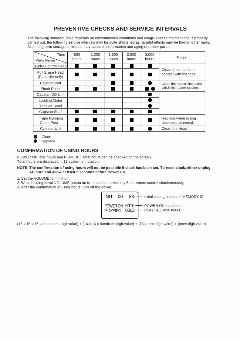
PREVENTIVE CHECKS AND SERVICE INTERVALS
The following standard table depends on environmental conditions and usage. Unless maintenance is properlycarried out, the following service intervals may be quite shortened as harmful effects may be had on other parts.Also, long term storage or misuse may cause transformation and aging of rubber parts.
Parts Name
Audio Control Head
NotesTime 500
hours1,000hours
1,500hours
2,000hours
3,000hours
: Clean: Replace
Full Erase Head(Recorder only)
Capstan Belt
Pinch Roller
Capstan DD Unit
Loading Motor
Tension Band
Capstan Shaft
Tape RunningGuide Post
Cylinder Unit
Clean those parts incontact with the tape.
Clean the rubber, and partswhich the rubber touches.
Replace when rollingbecomes abnormal.
Clean the Head
CONFIRMATION OF USING HOURSPOWER ON total hours and PLAY/REC total hours can be checked on the screen.Total hours are displayed in 16 system of notation.
NOTE: The confirmation of using hours will not be possible if clock has been set. To reset clock, either unplugAC cord and allow at least 5 seconds before Power On.
1.2.3.
Set the VOLUME to minimum.While holding down VOLUME button on front cabinet, press key 6 on remote control simultaneously.After the confirmation of using hours, turn off the power.
INIT 00 83
00100003
POWER ONPLAY/REC
Initial setting content of MEMORY IC.
POWER ON total hours.PLAY/REC total hours.
(16 x 16 x 16 x thousands digit value) + (16 x 16 x hundreds digit value) + (16 x tens digit value) + (ones digit value)

PREVENTIVE CHECKS AND SERVICE INTERVALS
CLEANINGNOTE
After cleaning the heads with isopropyl alcohol, do notrun a tape until the heads dry completely. If the headsare not completely dry and alcohol gets on the tape,damage may occur.
1. AUDIO CONTROL HEAD
Wrap a piece of chamois around your finger. Dip it inisopropyl alcohol and clean the audio control head bywiping it horizontally. Clean the full erase head in thesame manner. (Refer to the figure below.)
Audio Control Head
2. TAPE RUNNING SYSTEM
When cleaning the tape transport system, use thegauze moistened with isopropyl alcohol.
3. CYLINDER
Wrap a piece of chamois around your finger. Dip it inisopropyl alcohol. Hold it to the cylinder head softly.Turn the cylinder head counterclockwise to clean it (inthe direction of the arrow). (Refer to the figure below.)
NOTE
Do not exert force against the cylinder head. Do not movethe chamois upward or downward on the head.Use the chamois one by one.
Cylinder Head
3.
4.5.6.7.8.The unit will now have the correct DATA for the new MEMORY IC.
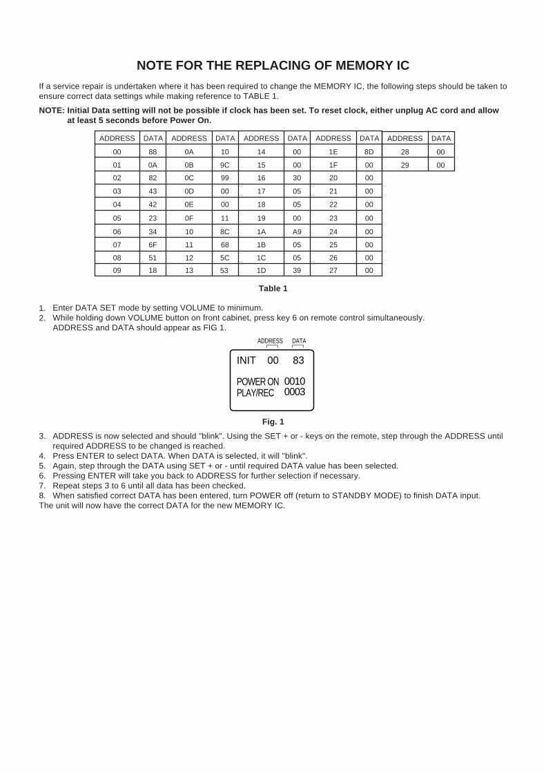
NOTE FOR THE REPLACING OF MEMORY IC
If a service repair is undertaken where it has been required to change the MEMORY IC, the following steps should be taken toensure correct data settings while making reference to TABLE 1.
NOTE:
Table 1
1.2.
Fig. 1
ADDRESS is now selected and should "blink". Using the SET + or - keys on the remote, step through the ADDRESS untilrequired ADDRESS to be changed is reached.Press ENTER to select DATA. When DATA is selected, it will "blink".Again, step through the DATA using SET + or - until required DATA value has been selected.Pressing ENTER will take you back to ADDRESS for further selection if necessary.Repeat steps 3 to 6 until all data has been checked.When satisfied correct DATA has been entered, turn POWER off (return to STANDBY MODE) to finish DATA input.
Enter DATA SET mode by setting VOLUME to minimum.While holding down VOLUME button on front cabinet, press key 6 on remote control simultaneously.ADDRESS and DATA should appear as FIG 1.
INIT 00 83
00100003
POWER ONPLAY/REC
ADDRESS DATA
Initial Data setting will not be possible if clock has been set. To reset clock, either unplug AC cord and allowat least 5 seconds before Power On.
ADDRESS DATA
00 88
01 0A
02 82
03 43
04 42
05 23
06 34
07 6F
08 51
09 18
ADDRESS DATA
0A 10
0B 9C
0C 99
0D 00
0E 00
0F 11
10 8C
11 68
12 5C
13
ADDRESS DATA
14 00
15 00
16 30
17 05
18 05
19 00
1A A9
1B 05
1C 05
1D 39
ADDRESS DATA
1E 8D
1F 00
20 00
21 00
22 00
23 00
24 00
25 00
26 00
27 0053
ADDRESS DATA
28 00
29 00

Taper nut driver
70909228
SERVICING FIXTURES AND TOOLS
Back tension cassette gauge
70909103
Torque cassette gauge(KT-300NR)
70909199
AdapterDial Torque Gauge(10~90gf•cm)(60~600gf•cm)
JG154 Cable
JG162A Cable (8 Pins)JG162D Cable (11 Pins)JG162Y Cable (5 Pins)
Tentelometer
VTR cleaning kit VTR lubrication kit Grease JG002BJG002E
JG002F
JG153 X Value AdjustmentScrewdriver
JG022 Master Plane JG024A Reel Disk HeightAdjustment Jig
Part No. Remarks
JG002B VSR Torque, Brake Torque (S Reel/T Reel Ass'y)
JG002E Brake Torque (T Reel Ass'y)
JG002F VSR Torque, Brake Torque (S Reel)
JG153 X Value Adjustment
JG022/JG024A Reel Disk Height Adjustment
Used to connect the Syscon PCB and Main PCBJG162A/JG162D
Used to connect the Syscon PCB and CRT PCBJG162Y
Used to connect the test point of SERVICE and GROUNDJG154
Alignment Tape
ST-N5ST-NF

PREPARATION FOR SERVICINGHow to use the Servicing Fixture
1.2.
3.
4.
Unplug the connector CP353, CP502, CP820 and CP850, then remove the VCR Block from the set.Connect as shown in the below figure using the Service Fixture.• Connect the Syscon PCB to the Main PCB with the cable JG162A and JG162D.• Connect the Syscon PCB to the CRT PCB with the cable JG162Y.Short circuit between TP1001 and Ground with the cable JG154.(Refer to MAJOR COMPONENTS LOCATION GUIDE)The EOT, BOT and Reel Sensor do not work at this moment.At that time, the STOP/EJECT button is available to insert and eject the Cassette Tape.
Front Cabinet
CRT PCB
CP850CP502
CP820 Main PCB
JG162D
JG162Y
JG162A
CD850
CP601
CD810
To Ground
JG154
Syscon PCB
TP1001
MECHANICAL ADJUSTMENTS
1. CONFIRMATION AND ADJUSTMENTRead the following NOTES before starting work.
•
•
Place an object which weighs between 450g~500g onthe Cassette Tape to keep it steady when you want tomake the tape run without the Cassette Holder. (Do notplace an object which weighs over 500g.)When you activate the deck without the CassetteHolder, short circuit between TP1001 and GND. (Referto ELECTRICAL ADJUSTMENT PARTS LOCATIONGUIDE) In this condition the BOT/EOT/Reel Sensor willnot function.
1-3: CONFIRMATION OF PLAYBACK TORQUE ANDBACK TENSION TORQUE DURING PLAYBACK
Load a video tape (T-120) recorded in standard speedmode. Set the unit to the PLAY mode.Install the tentelometer as shown in Fig. 1-3 . Confirm thatthe meter indicates 20 ± 2gf in the beginning of playback.
1.
2.
• USING A TORQUE CASSETTE GAUGE (KT-300NR)
1.
2.
3.
After confirmation and adjustment of Tension Postposition (Refer to item 1-2) , load the torque cassettegauge (KT-300NR) and set to the PLAY mode.Confirm that the right meter of the torque tape indicates60~110gf•cm during playback in SP mode.Confirm that the left meter of the torque tape indicates25~40gf•cm during playback in SP mode.
Tentelometer
Video Tape
Guide RollerP1 Post
Fig. 1-3
CONFIRMATION AND ADJUSTMENT OF REELDISK HEIGHT
1-1:
1.2.
3.
4.
Turn on the power and set to the STOP mode.Set the master plane (JG022) and reel disk heightadjustment jig (JG024A) on the mechanism framework,taking care not to scratch the drum, as shown in Fig. 1-1-A.Confirm that "A" of the reel disk is lower than "B" of thereel disk height adjustment jig (JG024A) , and is higherthan "C". If it is not enough height, adjust to 10(+0.2, -0)mm with the height adjustment washer.Adjust the other reel in the same way.
1-2: CONFIRMATION AND ADJUSTMENT OF TENSIONPOST POSITION
1.2.
3.
Set to the PLAY mode.Adjust the Tension Adjust until the edge of the TensionArm is positioning within 0.5mm range from thestandard line center of Main Chassis.After this adjustment, confirm that the cut position islocated in "A" area as shown in Fig. 1-2-B . If it islocated in "B" area, adjust again.While turning the S Reel clockwise, confirm that theedge of the Tension Arm is located in the positiondescribed above.
Reel Disk Height Adjustment Jig(JG024A)
Fig. 1-1-A
Reel Disk
Height AdjustmentWasher2.6x4.7xT0.132.6X4.7xT0.25
(B)
(C)
Master Plane (JG022)
Fig. 1-1-B
(A)
10(+0.2, -0)mm
Master Plane (JG022)
Reel Disk HeightAdjustment Jig(JG024A)
Fig. 1-2-A
Standard line of Main Chassis
Tension Adjust
Tension Arm
0.5mm (Adjusting range)
Standard line center of Main Chassis
(A)
Cut Position
Fig. 1-2-B
(B)
Tension Adjust

MECHANICAL ADJUSTMENTS
1-4: CONFIRMATION OF VSR TORQUE
Operate within 4~5 seconds after the reel disk begins toturn.Install the Torque Gauge (JG002F) and Adapter (JG002B)on the S Reel. Set to the Rewind mode. (Refer to Fig.1-4)Then, confirm that it indicates 120~180gf•cm.
1.
2.
3.
NOTE
Install the Torque Gauge on the reel disk firmly. Press theREW button to turn the reel disk.
1-5: CONFIRMATION OF REEL BRAKE TORQUE
(S Reel Brake) (Refer to Fig. 1-4)
Set to the STOP mode.Move the Idler Ass'y from the S Reel.Install the Torque Gauge (JG002F) and Adapter(JG002B) on the S Reel. Turn the Torque Gauge(JG002F) clockwise.Then, confirm that it indicates 60~100gf•cm.
1.2.3.
4.
(T Reel Brake) (Refer to Fig. 1-4)
Set to the STOP mode.Move the Idler Ass'y from the T Reel Ass'y.Install the Torque Gauge (JG002E) and Adapter(JG002B) on the T reel. Turn the Torque Gauge(JG002E) counterclockwise.Then, confirm that it indicates 45~70gf•cm.
1.2.3.
4.
NOTE
If the torque is out of the range, replace the followingparts.
Check item
1-4
1-5
Replacement Part
Idler Ass'y/Clutch Ass'y
T Brake Spring/Tension Spring
2. CONFIRMATION AND ADJUSTMENTOF TAPE RUNNING MECHANISM
Tape Running Mechanism is adjusted precisely at thefactory. Adjustment is not necessary as usual. When youreplace the parts of the tape running mechanism becauseof long term usage or failure, the confirmation andadjustment are necessary.
2-1: GUIDE ROLLER
Playback the Alignment Tape.Connect CH-1 of the oscilloscope to TP4001 (Envelope)and CH-2 to TP1002 (SW Pulse) .Press and hold the TRACKING-AUTO button on theremote control more than 2 seconds to set tracking tocenter.Trigger with SW Pulse and observe the envelope. (Referto Fig. 2-1-A)When observing the envelope, adjust the Taper NutDriver slightly until the envelope will be flat.Even if you press the Tracking Button, adjust so thatflatness is not moved so much.Adjust so that the A : B ratio is better than 3 : 2 as shownin Fig. 2-1-B , even if you press the Tracking Button tomove the envelope (The envelope waveform will begin todecrease when you press the Tracking Button).Adjust the PG shifter during playback.(Refer to the ELECTRICAL ADJUSTMENTS)
1.2.
3.
4.
5.
6.
7.
NOTE
After adjustment, confirm and adjust A/C head.(Refer to item 2-2)
Fig. 2-1-A
Max
A : B = 3 : 2
A
Entrance Exit
MaxB
Fig. 2-1-B
CH-2SW Pulse (TP1002)
CH-1Track
CH-2Track
CH-1Envelope(TP4001)
Envelope
CH-3Audio
(1)
(2)
Fig. 1-4
Torque Gauge/Adapter(JG002F/JG002B)
T Reel
S Reel
Torque Gauge/Adapter(JG002E/JG002B)
MECHANICAL ADJUSTMENTS
2-3:2-2:
When the Tape Running Mechanism does not work well,adjust the following items.
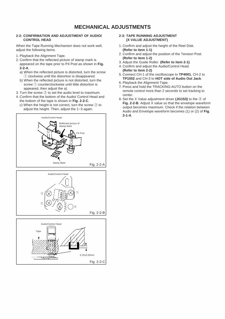
CONFIRMATION AND ADJUSTMENT OF AUDIO/CONTROL HEAD
1.2.
3.4.
Playback the Alignment Tape.Confirm that the reflected picture of stamp mark isappeared on the tape prior to P4 Post as shown in Fig.2-2-A.a)
b)
Turn the screw 2 to set the audio level to maximum.Confirm that the bottom of the Audio/ Control Head andthe bottom of the tape is shown in Fig. 2-2-C .c)
TAPE RUNNING ADJUSTMENT(X VALUE ADJUSTMENT)
Confirm and adjust the height of the Reel Disk.(Refer to item 1-1)Confirm and adjust the position of the Tension Post.(Refer to item 1-2)Adjust the Guide Roller. (Refer to item 2-1)Confirm and adjust the Audio/Control Head.(Refer to item 2-2)Connect CH-1 of the oscilloscope to TP4001, CH-2 toTP1002 and CH-3 to HOT side of Audio Out Jack .Playback the Alignment Tape.Press and hold the TRACKING-AUTO button on theremote control more than 2 seconds to set tracking tocenter.Set the X Value adjustment driver (JG153) to the 4 ofFig. 2-2-B . Adjust X value so that the envelope waveformoutput becomes maximum. Check if the relation betweenAudio and Envelope waveform becomes (1) or (2) of Fig.2-1-A.
1.
2.
3.4.
5.
6.7.
8.
When the reflected picture is distorted, turn the screw1 clockwise until the distortion is disappeared.When the reflected picture is not distorted, turn thescrew 1 counterclockwise until little distortion isappeared, then adjust the a).
When the height is not correct, turn the screw 3 toadjust the height. Then, adjust the 1~3 again.
Reflected picture ofStamp Mark
Stamp Mark
Audio/Control Head
P4 Post
Fig. 2-2-A
Audio/Control Head
13
2
Fig. 2-2-B
Tape
Audio/Control Head
Fig. 2-2-C
0.25±0.05mm
4

MECHANICAL ADJUSTMENTS
3. MECHANISM ADJUSTMENT PARTS LOCATION GUIDE
5
6
7
8
910
1
2
3
4
1. Tension Adjust2. Tension Arm3. Guide Roller4. P1 Post5. Audio/Control Head
6.7.8.9.
10.
X value adjustment driver holeP4 PostT Brake SpringT ReelS Reel

ELECTRICAL ADJUSTMENTS
1. ADJUSTMENT PROCEDURERead and perform these adjustments when repairing thecircuits or replacing electrical parts or PCB assemblies.
CAUTION
2. BASIC ADJUSTMENTS
(VCR SECTION)2-1: PG SHIFTER
1.
2.3.
4.
Connect CH-1 on the oscilloscope to TP1002 and CH-2to TP4201.Playback the alignment tape.Press and hold the Tracking-Auto button on the remotecontrol more than 2 seconds to set tracking to center.Press the VOL. DOWN button on the set and thechannel button (3) on the remote control simultaneouslyuntil the indicator REC disappears. If the indicator RECdisappears, adjustment is completed.
(If the above adjustments doesn't work well:)
5.
6.
7.
Press the VOL. DOWN button on the set and thechannel button (3) on the remote control simultaneouslyuntil the indicator REC disappears.When the REC indicator is blinking, press both VOL.DOWN button on the set and the channel button (4) onthe remote control simultaneously and adjust theTracking +/- button until the arising to the down of HeadSwitching Pulse becomes 6.5 ± 0.5H.(Refer to Fig. 2-1-A, B)Press the Tracking Auto button.
Fig. 2-1-B
CH-2
CH-1
6.5H
CH-1
CH-2
6.5H
Fig. 2-1-A
2-2: VCO FREERUN
1.2.
3.
4.
Place the set with Aging Test for more than 10 minutes.Connect the digital voltmeter between the pin 7 ofCP602 and the pin 1 (GND) of CP602 .Activate the adjustment mode display of Fig. 1-1 andpress the channel button (03) on the remote control toselect "VIF VCO".Press the VOL. UP/DOWN button on the remote controluntil the digital voltmeter is 2.5 ± 0.5V.
•
•
•
•
Use an isolation transformer when performing anyservice on this chassis.Before removing the anode cap, discharge electricitybecause it contains high voltage.When removing a PCB or related component, afterunfastening or changing a wire, be sure to put the wireback in its original position.Inferior silicon grease can damage IC's and transistors.When replacing IC's and transistors, use only specifiedsilicon grease.Remove all old silicon before applying new silicon.
On-Screen Display Adjustment
1.
2.
Unplug the AC plug for more than 5 seconds to set theclock to the non-setting state. Then, set the volumelevel to minimum.Press the VOL. DOWN button on the set and thechannel button (9) on the remote controlsimultaneously to display adjustment mode on thescreen as shown in Fig. 1-1 .
Fig. 1-1
Use the Channel UP/DOWN button or Channel button(0-9) on the remote control to select the options shownin Fig. 1-2 .Press the MENU button on the remote control to endthe adjustments.
3.
4.
FUNCTIONOSD HCUT OFFRF DELAYVIF VCOH VCOH PHASEV SIZEV SHIFTR DRIVEB DRIVER CUT OFFG CUT OFFB CUT OFF
NO.00010203040506070809101112
FUNCTIONBRIGHTNESSCONTRASTCOLORTINTSHARPNESSFM LEVELLEVELSEPARATION 1SEPARATION 2TEST MONOTEST STEREOX-RAY TEST
NO.131415161718192021222324
TV
00 OSD 15
Fig. 1-2

ELECTRICAL ADJUSTMENTS
2-3: RF AGC
1.2.
3.
4.
Receive the VHF HIGH (70dB).Connect the digital voltmeter between the pin 5 ofCP602 and the pin 1 (GND) of CP602 .Activate the adjustment mode display of Fig. 1-1 andpress the channel button (02) on the remote control toselect "RF DELAY".Press the VOL. UP/DOWN button on the remote controluntil the digital voltmeter is 2.65 ± 0.05V.
2-7: WHITE BALANCE
NOTE: Adjust after performing CUT OFF adjustment.
1.2.3.
4.
5.
6.
7.
8.
Place the set with Aging Test for more than 15 minutes.Receive the color bar pattern.Using the remote control, set the brightness and contrastto normal position.Activate the adjustment mode display of Fig. 1-1 andpress the channel button (10) on the remote control toselect "R CUT OFF".Using the VOL. UP/DOWN button on the remote control,adjust the R CUT OFF.Press the CH. UP/DOWN button on the remote control toselect the "R DRIVE", "B DRIVE", "G CUT OFF" or "BCUT OFF".Using the VOL. UP/DOWN button on the remote control,adjust the R DRIVE, B DRIVE, G CUT OFF or B CUTOFF.Perform the above adjustments 6 and 7 until the whitecolor is looked like a white.
2-8: FOCUS
1.2.3.
Receive the monoscope pattern.Turn the Focus Volume fully counterclockwise once.Adjust the Focus Volume until picture is distinct.
2-9: HORIZONTAL PHASE
1.2.
3.
4.
Receive the monoscope pattern.Using the remote control, set the brightness andcontrast to normal position.Activate the adjustment mode display of Fig. 1-1 andpress the channel button (05) on the remote control toselect "H PHASE".Press the VOL. UP/DOWN button on the remotecontrol until the SHIFT quantity of the OVER SCAN onright and left becomes minimum.
(TV SECTION)2-4: CONSTANT VOLTAGE
1.2.3.4.5.
6.
Input DC12V to DC Jack and turn the Power ON.Connect the digital voltmeter to the TP401.Set condition is AV MODE without signal.Adjust the VR501 until the DC voltage is 101 ± 0.5V.Input AC120V to AC cord and remove the DC Jackcord. Check if the Power is ON before doing the aboveprocedure.Adjust the VR502 until the DC voltage is 102 ± 0.5V.
2-10: VERTICAL SIZE
NOTE: Adjust after performing adjustments in section 2-9.
1.
2.
3.
4.
5.
Receive the cross hatch signal from the PatternGenerator.Using the remote control, set the brightness andcontrast to normal position.Activate the adjustment mode display of Fig. 1-1 andpress the channel button (06) on the remote control toselect "V SIZE".Press the VOL. UP/DOWN button on the remotecontrol until the rectangle on the center of the screenbecomes square.Receive a broadcast and check if the picture is normal.
2-5: OSD HORIZONTAL
1.2.
Activate the adjustment mode display of Fig. 1-1 .Press the VOL. UP/DOWN button on the remotecontrol until the difference of A and B becomesminimum. (Refer to Fig. 2-2)
BA
TV
00 OSD 15
Fig. 2-2
1.
2.3.4.
5.
Adjust the unit to the following settings.R CUT OFF=128, G CUT OFF=128, B CUT OFF=128,R DRIVE=64, B DRIVE=64, BRIGHTNESS=128,CONTRAST=96Place the set with Aging Test for more than 15 minutes.Set condition is AV MODE without signal.Activate the adjustment mode display of Fig. 1-1 andpress the channel button (01) on the remote control toselect "CUT OFF".Adjust the Screen Volume until a dim raster is obtained.
2-6: CUT OFF
ELECTRICAL ADJUSTMENTS
2-11: VERTICAL POSITION
NOTE: Adjust after performing adjustments in section 2-10.
1.
2.
3.
4.
Receive the center cross signal from the PatternGenerator.Using the remote control, set the brightness andcontrast to normal position.Activate the adjustment mode display of Fig. 1-1 andpress the channel button (07) on the remote control toselect "V POSI".Press the VOL. UP/DOWN button on the remotecontrol until the horizontal line becomes fit to the notchof the shadow mask.
2-12: SUB BRIGHTNESS
1.2.
3.
4.
5.6.
Receive the monoscope pattern.Using the remote control, set the brightness andcontrast to normal position.Activate the adjustment mode display of Fig. 1-1 andpress the channel button (13) on the remote control toselect "BRIGHTNESS".Press the VOL. UP/DOWN button on the remotecontrol until the white 5% is starting to be visibleReceive the monoscope pattern. (Audio Video Input)Press the TV GAME button on the remote control to setto the AV mode. Then perform the above adjustments2~4.
2-13: SUB TINT
1.2.
3.4.
5.
6.7.
Receive the color bar pattern. (RF Input)Using the remote control, set the brightness, contrast,color and tint to normal position.Connect the synchro scope to TP803.Activate the adjustment mode display of Fig. 1-1 andpress the channel button (16) on the remote control toselect "TINT".Press the VOL. UP/DOWN button on the remotecontrol until the section "A" becomes a straight line.(Refer to Fig. 2-3)Receive the color bar pattern. (Audio Video Input)Press the TV GAME button on the remote control to setto the AV mode. Then perform the above adjustments2~5.
Fig. 2-3
"A"
2-14: SUB COLOR
1.2.
3.4.
5.
6.
7.8.
Receive the color bar pattern. (RF Input)Using the remote control, set the brightness, contrast,color and tint to normal position.Connect the synchro scope to TP801.Activate the adjustment mode display of Fig. 1-1 andpress the channel button (15) on the remote control toselect "COLOR".Adjust the VOLTS RANGE VARIABLE knob of theoscilloscope until the range between white 100% and0% is set to 5 scales on the screen of the oscilloscope.Press the VOL. UP/DOWN button on the remotecontrol until the red color level is adjusted to 120 ± 5%of the white level. (Refer to Fig. 2-4)Receive the color bar pattern. (Audio Video Input)Press the TV GAME button on the remote control to setto the AV mode. Then perform the above adjustments2~6.
0%
Fig. 2-4
White 0%
White 100%
100%
Red Level

ELECTRICAL ADJUSTMENTS
3. ELECTRICAL ADJUSTMENT PARTS LOCATION GUIDE
(VCR SECTION)
SYSCON PCB
TU601
TP4201J4202 J4201
TP4001
TP1001
CP602
TP1002

ELECTRICAL ADJUSTMENTS
(TV SECTION)
MAIN PCB
FOCUS VOLUMESCREEN VOLUME
FB401T502
T501VR501
VR502
TP401
J801
TP801
TP803
CRT PCB

ELECTRICAL ADJUSTMENTS
4. PURITY AND CONVERGENCEADJUSTMENTS
NOTE
1.
2.
3.
Turn the unit on and let it warm up for at least 30minutes before performing the following adjustments.Place the CRT surface facing east or west to reduce theterrestrial magnetism.Turn ON the unit and demagnetize with a Degauss Coil.
4-1: STATIC CONVERGENCE (ROUGH ADJUSTMENT)
1.
2.
3.
4.
5.
6.
7.
8.
Tighten the screw for the magnet. Refer to the adjustedCRT for the position. (Refer to Fig. 4-1)If the deflection yoke and magnet are in one body,untighten the screw for the body.Receive the green raster pattern from the color bargenerator.Slide the deflection yoke until it touches the funnel sideof the CRT.Adjust center of screen to green, with red and blue onthe sides, using the pair of purity magnets.Switch the color bar generator from the green rasterpattern to the crosshatch pattern.Combine red and blue of the 3 color crosshatch patternon the center of the screen by adjusting the pair of 4pole magnets.Combine red/blue (magenta) and green by adjusting thepair of 6 pole magnets.Adjust the crosshatch pattern to change to white byrepeating steps 6 and 7.
4-2: PURITY
NOTE
Adjust after performing adjustments in section 4-1.
1.
2.
3.
4.5.
Receive the green raster pattern from color bargenerator.Adjust the pair of purity magnets to center the color onthe screen.Adjust the pair of purity magnets so the color at theends are equally wide.Move the deflection yoke backward (to neck side)slowly, and stop it at the position when the whole screenis green.Confirm red and blue colors.Adjust the slant of the deflection yoke while watchingthe screen, then tighten the fixing screw.
DEFLECTION YOKEDEFLECTION YOKE SCREWMAGNET SCREW
6 POLE MAGNETS4 POLE MAGNETSPURITY MAGNETS
Fig. 4-1
4-3: STATIC CONVERGENCE
NOTE
Adjust after performing adjustments in section 4-2.
1.
2.
3.
Receive the crosshatch pattern from the color bargenerator.Combine red and blue of the 3 color crosshatch patternon the center of the screen by adjusting the pair of 4pole magnets.Combine red/blue (magenta) and green by adjusting thepair of 6 pole magnets.
4-4: DYNAMIC CONVERGENCE
NOTE
Adjust after performing adjustments in section 4-3.
1.
2.
Adjust the differences around the screen by moving thedeflection yoke upward/downward and right/left.(Refer to Fig. 4-2-a)Insert three wedges between the deflection yoke andCRT funnel to fix the deflection yoke.(Refer to Fig. 4-2-b)
R G B
RGB
R G B
RGB
UPWARD/DOWNWARD SLANT RIGHT/LEFT SLANT
Fig. 4-2-a
WEDGE WEDGE
WEDGE
WEDGE POSITION
Fig. 4-2-b

MICON/DECK
Q806
BLUE AMP
Q805
GREEN AMP
Q804
RED AMP
Q405
H-DRIVE
Q406
H. OUTPUT DY
7
V. OUTPUT IC401 LA78040
3
THERMALPROTECTION
PUMPUP
5VCC
AMP
2
7 F
S9
2 HV
7
9
F
8
3
J801
V801CRT
1
SP351SPEAKER
SOUND AMP IC351 AN7511
6
8
2
VCR_POWER-H
5
MICON/DECK
4
TV_A_MUTE
1
HD
OSD_G
AFT_M
OSD_B
OSD_R
OSD_BLK
VD
COL+B
ABL
AFC
CHROMAIC601 M61203CFP
57
62
1
64
26
VIF AMP
APC DET
BLACK STRETCH GAMMA
LOCK DET
CHROMA TRAP
CHROMA BPF
BRIGHT DRIVE AMP
5
16
15
14CLAMP
10
3536 34
31
60
IF AGC
63 48
DELAY ADJ
56
VCORF AGC
VIDEO DET
AFT
VIDEO MUTE
DEFEAT AFT OUT
CLAMP
VIDEO TONE
DELAY
55
5.7Vreg
41
RESET
42 33 39 46 13
POWER ON CONTROL
RGB MATRIX
CONTRAST
HPF
ACC
KILLERDET
ACC DET
CHROMA APCDET
DEMODULATOR
VCXO
VCOADJ
32
HVBLK
VERTICAL COUNT DOWN V.RAMP
29
17
HORIZONTALCOUNT DOWN
H VCO AFC 2AFC 1
76
R G BCUT OFF
BUS I/F
TU601
11
5
4
1SAW FILTERCF601
1 54
CHROMA_VIDEO
Y/C_AUDIO
TU_AUDIO
TU_VIDEO
SDASCLMICON/
DECK
AT+5V
X6023.579545MHz
53
Q610, Q611
REG
Q606
Q602, Q603
50
1
27
TV_POWER-H
HEADPHONE JACK
J351
FB401
NC
P-ON-ON
REG
REG
52
12
AT+13V
P.CON+5V
P.CON+8V
3 +25V
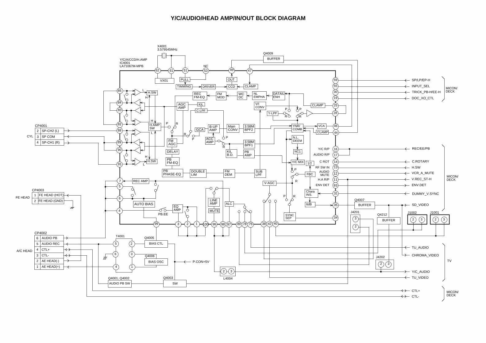
Y/C/AUDIO/HEAD AMP/
IN/OUT
Y/C/AUDIO/HEAD AMP/
IN/OUT
TV BLOCK DIAGRAM
6
L508DEGAUSSCOIL
Q402Q401
DEGAUSSDRIVE
DEGAUSSSW
+180V
T501
5
7
11.3V REG.OPE AMP
IC504 FA7610CP
4
5
3
1
T502
3
7
8
15
13
9
Q505
IC506 TLP621FEED BACK 1
POWER REG.IC501STR-G6623
5
Q512
Q509
DC INRY503 RELAY
J503 DC JACK
Q511
SW
REG. DRIVER
REG. DRIVER
4
11
15
16
14
10Q508
PROTECTOR
Q515
PROTECTOR POWER FILE(DC)
Q503
PROTECTOR
Q507FEED BACK
SW
Q504
PROTECTOR
Q513
VR
502
AC
+B
AD
J
5V SW.
VR
501
DC
+B
AD
J
UNREG+8V
AT+12V
AC IN
F501 D503, D504D535, D536RECTIFIER
PROTECTORQ518
PROTECTORQ514
6
DC POWERSW
X40013.579545MHz
40100 98 97
25
4296
28
85
83
82
5
7
46
4
6
44
59
55
30
19
14
13
93
2 13 78 76
H.AMPSW
REC AMP
CP4001
4
3
2
SP-CH1 (R)
SP COM
SP-CH2 (L)
CYL
FE HEAD (HOT)
FE HEAD (GND)2
1
CP4003
FE HEAD
CP4002
6
5
4
AUDIO PB
AUDIO REC
CTL+A/C HEAD3
2
1
AE HEAD(-)
AE HEAD(+)
CTL-
CTL+
CTL-
Y/C/A/CCD/H.AMPIC4001LA71067M-MPB
49
Q4009
BUFFER
VX01
62 61
PULL
51
TIMMING
53
CCD
OUT
DRIVER CLAMP
47
16
17
12
11
34
31
35
84
H.SW
88
90
91
89
H.SW
H
L
H
L
H
L
PB.EE
P
R
WCDC
DATAILENH
NLEMPHA
RECFM-EQ
FMMOD
P R
AGCAMP
KIL
FMAGC
DELAY
PBFM-EQ
PBPHASE-EQ
P
R
C-LPF
GCAB-UPAMP
ACCAMP
MainCONV
3.58MBPF2
AUTO BIAS
P
R
KILB.D.
PBAMP
3.58MBPF1
DOUBLELIM
FMDEM
SUBLPF
V/ICONV
P
RY-LPF
YNR/COMB
N.L.DEEM
NC1
Y/C MIX
SYNCSEP
VCA
CLAMP
1/2
FBC
CharaINS.
6dB
P R
P
RV-AGC
T4001
CLAMP
EQAMP
LINEAMP
MUTE
ALC
SP/LP/EP-H
INPUT_SEL
TRICK_PB-H/EE-H
DOC_XO_CTL
REC/EE/PB
C.ROTARY
H.SW
VCR_A_MUTE
V.REC_ST-H
ENV.DET
DUMMY_V.SYNC
SD_VIDEO
TU_VIDEO
TU_AUDIO
MICON/DECK
6
2
3
1
5
Q4006
BIAS OSC
Q4005
BIAS CTL
99
Q4003
SW
Q4001, Q4002
AUDIO PB SW
4
P.CON+5V
Y/C R/P
AUDIO R/P
C ROT
RF SW INAUDIOMUTE
H.A R/P
ENV DET
2 3
L4004
NC
Q4007
BUFFER
MICON/DECK
MICON/DECK
3880
J4201
3
2
TV
32
J1002
32
J4202
Q4212
BUFFER
Y/C_AUDIO
CHROMA_VIDEO
Y/C/AUDIO/HEAD AMP/IN/OUT BLOCK DIAGRAM
32
J1001

66
56
V-REC-ST-H
CVIN
27
76
90
89
VCR-POWER
CAP-PWM
DRUM-PG
DRUM-FG
X-OUT(12MHz) 39
35XC-IN(32MHz)
85POWER_FAIL_L
72IIC-DATA1
TIMER SYSCON SERVO MICONIC1001 OEC7043B
38X-IN(12MHz)
36XC-OUT(32KHz)
77 DRUM-PWM
71IIC-CLK1
94CTL-
95CTL+
62
7
OSD B
AFT(MONI)
63OSD G
64OSD R
59
58
V-SYNC
H/C-SYNC
60OSD OUT1
30
29
REC LED
T-REC LED
9KEY A
14REMOCON-IN
28TV-POWER
10KEY B
34 RESET-L
87
11
CAP-FG
CAP-FWD
50
80
79
REEL-T
REEL-S
TAB SW
321
OS1001
AT + 5V
CH DOWN CH UP VOL. UP VOL. DOWN
POWERON/OFF REC/OTR STOP/EJECT PLAY FF/CUE REW/REV
X100112MHz
X100232.768KHz
3OUT IC1002PST600H
6
5 SDA
SCL EEP ROMIC1099S-24C04BDP-LA
SW1001
D793
D791 D792
Q4205
REC LED SW
Q4206T-REC
LED SW
2 3
41
5 CYL DRIVE
7
6
CAP.M F/RFG
3 CYL FG1 CYL PG
CP1005
4 CTLCP1004
1 3
42
1 3
42
REEL SENS.Q1005
REEL SENS. Q1001
POWER FAIL(DC)
SDA
SCL
OSD_R
CTL+
SD_VIDEO
CTL-
V. REC_ST_H
VD
OSD_G
AFT_M
OSD_B
OSD_BLK
HD
Y/C/AUDIO/HEAD AMP/IN/OUT
TV
CAPSTANDD UNIT
MICROMOTOR
TV_POWER_H
FF/REW-L
97
73
CTL AMP-OUT Q1004
FF/REW_SW
18VIDEO-H.SW H. SW
VCR_POWER_HTV
Q4204
TV POWERSW
82TV_A_MUTE TV_A_MUTE
23
2
1
MS SENS LED
MSSEN-B
MSSEN-A1 4
32
1 4
32Q1002
SENSOR SW
MS_SEN AQ1009
MS_SEN BQ1003
AT + 5V
P. CON + 5V
68 CENTER LED
Q1024
LED DRIVERP. CON + 5V
EOT3
LDM-RVS
LDM-FWD 21
20
BOT 4
POWERSAVE
CONTROL LOGIC
STD
2 5 7 4
LOADING MOTOR DRIVERIC1003 BA6955N
P. CON + 5V
LDM-
LDM+
BOT
3
4
2
CP1006
VCC1
LDM-
LDM+
BOT
2
1
3
CP101
VCC 4
BOT SENSORQ101
LM
M101
LOADINGMOTOR
REC/OTR
T-REC
PO
WE
R
61REC-H/EE-M/PB-L
67YC DOC/XO-CTL
83SP/LP/EP-H
69TRICK_PB-H
6VIDEO-ENV-DET
81VCR_A_MUTE
15 COLOR ROTARYC_ROTARYY/C/AUDIO/HEAD AMP/IN/OUT
13 DUMMY-V.SYNCDUMMY_V.SYNC
33 INPUT_SELCTINPUT_SEL
REC/EE/PB
DOC_XO_CTL
SP/LP/EP-H
TRICK_PB-H/EE-H
ENV_DET
VCR_A_MUTE
INPUTSELECT
TV
MICON/DECK BLOCK DIAGRAM
D1003
21
VCC
EOTCP1002
SYSTEM RESET
21
VCC
EOTCP102
BOT SENSORQ102
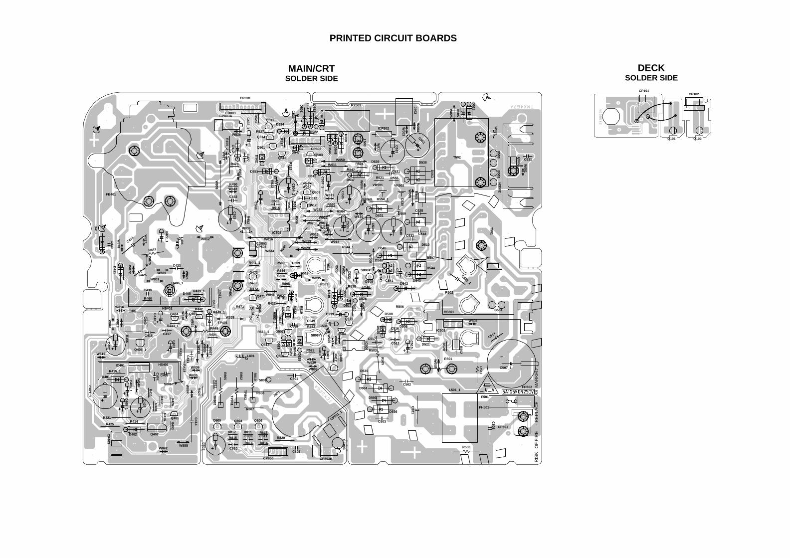
PRINTED CIRCUIT BOARDS
MAIN/CRTSOLDER SIDE
FB401
D413
C430
C438
C406_1
C404
R416
C403
R415_1
C405_1
CP
403
R425
C409
T401
W884
C418_1
C416
C440
R447
W878
L401
C422_1
W824
R490
R423
D412
C433_1
R450_2
R453
TP401
Q401
R403
D409
D408
CP820
W877
W041
C417
R421
R456
Q408
R401
R460
D402
W042
W035
R420
R440_1Q407Q404R442
R443_1
R439_1
R441_1
W810
R417
R419
W037
W036
W034
R410
CP803A
R422
J503
W003
W001
Q505
C514
R511
IC506
C521
FH502
F501
FH501
CP501
C505
D536
C503
D503
D504
D535C507_1
B502
L501_1
C513
C510
R502
R506
C516
D534
D508
R503
D521
D506
B501
B503
D518D
505
R505
C502
C523_1
RY503
ICP502
L503 C
515
C551
IC504
R547
C540
D509
D510
B505_1
B507
C518
C525
C535
D553
D538
D543
D544
D545
D531
C530
C532
C533
D542
D537
D541
D540
R524
VR502VR501
CP502
D516
R554_1
R504
W006
Q508
C522
R538
R545
D513
D546
D548D547
T501
R540
W008R
531
R518 Q512
R539
R522
C508
R515
R507
R508
C506
R527
Q514
D524
R517
Q501
Q518
D502
D512
W016
D527
D530
R533
R519
D519
D520
R532
R552
C549
Q507
D529 D
523
Q506
R513_1
R516
R529
R536
W027
W803
J801
CP803B
CP801_1
CP850
R805
R810
R802
S801
Q806Q804Q805
R820
R807
R808
R816R814
R815
R813R811
L801
TP
801
TP
802
TP
803
C809
C810
C811
C805
C801
R553_1
C411
R424
R535
HS402
Q406_1
W030
CP
401
Q402
W040C
421_1
W815
R544_1
D401
Q509
C423
HS
502
R528
C509
D539
D526
Q504
W007
W819
R411
R500
R512
Q511
R523
IC401 HS401
W029
W032
CC
003
C414
Q405_1
W889
W021
R449
R501
W813
R426
C424
C517
C512
C504_2
W022
D549
R414
W875
D411
C427
D550
R404
C531
W825
W039 Q515
T502
D517
W827
W826
W816
W005
C541
W004
C402
W015
IC501
HS501
W805
W009
W831
W011
R509
D528
C803
CP503
W020
W026
W019
W017W018
W014
W833
W013
R812
C538
C539
W044
C555
W888
Q513
W046
D501
D552
C528
W809
B504
R555
D522
D551
W047
R821
R430
R413
C537_1
Q503W050
D515
C544
C407
C534_2
C536_1
R521
W822
C511
W051
C432
W823
W835
W844
W839
W838
W801
W818
W812
CD803
S808Y
S808X
S806X
S806Y
W872
C425
W830
W842
C410 R
412
R556
W045
R471
Q472
Q471
R472
R473
CD503
C529
RIS
KO
FF
IRE
-R
EP
LAC
EA
SM
AR
KE
D.
CP101
Q101 Q102
CP102
DECKSOLDER SIDE

PRINTED CIRCUIT BOARDSSYSCON (INSERTED PARTS)
SOLDER SIDE
CP1004
SW
1012S
W1003
SW
1011
SW
1002S
W1005
OS
1001
C1004
SW
1007S
W1008
SW
1009S
W1010
SW
1006
SW
1004SW1001
IC1003
CP
1006
CP1005_1
D1002
W084
W087
W088
W037
W066
W816
W181
D1003
C1015
W076
X1002
W148
R1005
D1001
R1016
W131
W081
W133
C1016
C1018
D4207
C1003_1
W060
IC1099
W075
W078
X1001
W086
D1005
R1009
R1013
W019
W026
W034
IC1002
W129
W152
C1001
W072
W071
W070
W069
W122
L1001
W068
W065
C1020
W080
C1021
W126
R1079
W011
W123W074
W012
W007
R1010
W147
CP
4002
W109
W128
W067
R1047
W192
R610
TP
1001
TP
1002
TP
4001
R1002
CC4201
CC4202
R1046
R1040
W028
W808
W079
Q1003
Q1009
W004
W094
W073
W063
W061
W132
W135
W136
W140
W137
W139
W142
W025
W107W
108
W124
W121
W125
R1024
R1028
W146
CP
602
W003
W064
W058
W141
W006
W008
W194
W187
W151
TU601
C610
IC1101
Q1102
Q603
Q606
Q610
Q611
Q602
C1102
C643
L603
C612
TP
4201
C4211
D4206
R4239
L4205
C4220
C4209
C670
C652
D610
D1101
W089
C601
W021
W022
Q1005
Q1001
W143
W048
W110
W145
W144
J4202J4201
W204
W203
W202
W201
W246
W245
W241
C4241
W213
C4214
W239
W247
W248
W238
W185
W184
W240
CP1001
W130
W206
Q4005
Q4003
Q4002
Q4001
Q4006
T4001
C4011
C4021
C4023
C4031
C4037
C4039
C4070
C4033
C4045
C4015
C4017
C4016
L4004
L4005
C4034
C4035
C4043
W165
L4002
L4008
C4061
C4007
C4062
L4007
W099
L4001
W161
W102
W091
R4015
C4024
L4009R4052
W119
CP
4001_1
CP4003
L4010
C4071
W118
C4010
W117
W164
C4022
W836
W180
W158
W045
C4008
W046
C4030
X4001
C4057
W093
W869
W197
W098
L4003
W179
W221R351
C355
IC351 C356
C351
B301
R644
D605
W228
L608
C620
L607
CF604
D602D601
C624
C631
R625
C649
W227
W162
D612
D609
W178
C655
D615D614
D613
W195
C645
R607
R601
CF601 C635
W232
W236W
235
D607
C632
CF603 C659
X602
W217
W209
W208
W186W189W190
W183
W191
W243 W199
D618
D617
W198
D616
W176
W223
W224
W231
R638
W226
W234
W222
W210
W233
W200
W172W174
W166
W163
W167
W216
W212
W211
W214
W215
R4061
W154
W101
W105
W822
C4060
R4031
W168
R4070
W054
C4075
W097
W157
W169
W171
W113
W111
W112
W100
R4068
R4067
W115
D792
D791
D793
C1058
W050
W029
W023
D4208
R1039
D1014
W033
W082
W077
W085
W083
W149
D4209 D4210
W196
D4201
D608
W832
W042
W043
W044
W052W053
W013
W014
W015
C1032
J351
W096
W095
W055
W134
W237
W242
W018
W017
W002W
092
W051
W049
W062
W047
C4026
C4076
W005
W188
R1102
C673
R301
CP1002
CD810
CP601
CD850
W205
C4059
R4062
R360
W020
W103
R4054
R4045
D611
L614
R1001
L601_1
W225
W160
R353
W220
W219
W831
W173
W155
W024
W036
C357
C358
W837
W218
C4058
C664
R674
W116
W256
W114
W230B602
W244W844
B302
B303
W255
W177
C641
C354_1
W845
C4004
W253
W252
W251
CC001
C362
W254
W193
W182
R4075
C648_1
D619
W852
W850
D1004
W257
J1001J1002
C665_1
D620
W814
W827
W823
W810
W849
W834
W824
W851
W867
W821
W807 W841
L1002
W809
W813
W835
W803
W804
W847
W846
W801
W090
W027
CP353
R4201
W855
HS
1100
HS351
W856
R4077
C671
R665
S811Y
S811X
S810X
S810Y
S802Y
S802X
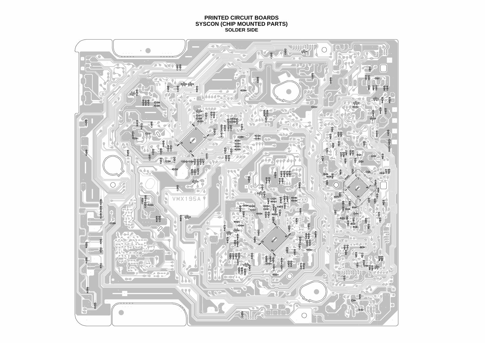
PRINTED CIRCUIT BOARDSSYSCON (CHIP MOUNTED PARTS)
SOLDER SIDE
R10
84R
1088
R10
96
R10
90
R10
91
R10
86
R10
80
R10
95
R10
89C1006
C10
08
C1041
C10
71
R1008
C10
61
R1007
C10
87
C1009
C1010
C10
23
C10
60
C10
68 C42
07
C1065
Q1024
C1034
R10
29
R10
53
R10
45
R1044
C10
33
C10
30
C10
39
R1051
C10
26
R10
66
Q4204
Q4206Q4205
R1035R1021
R1083
C1025 C10
22
C1027
R10
54
R10
87R
1050
C1017
C10
02
R10
03
R42
04
R1036
C10
29
C1028
C10
66
C10
13
C10
19R
1012
R10
06
R10
19
Q1002
Q1004
R10
17
R10
20
C10
40
C10
48 C10
49C
1050
C1046 C10
47
R1032
R10
31
R10
34R
1033
C10
31C
1038
C10
35IC
1001
C10
14
C10
62
R10
77
R10
49
C10
85
R10
18
R10
04
C10
05
R10
11
C42
04
C10
63
C60
9R
605
C60
4
C60
5C
613
Q4212
R42
38
Q4210
R4232
C42
10
Q4203
C60
2R
603
R60
2
R42
13
C42
06
C607
R40
80
R42
03C
4205
R42
36
R42
12
R42
44
R42
43
C10
44
C40
18R
4022
R4023
R40
01
IC40
01
C40
03
R4004
R40
02R
4003
C40
05R
4010
C40
06
C40
74
R40
11
R4020
R40
25
C4020
R40
27
R40
12
R4072
R40
07C
4002
R40
13R
4008
C40
25
R4032
R40
34
C4027
R40
47
C40
38
C40
41
C40
66R
4026
R40
19
R40
29
C40
65R
4028
R4033
C40
28
C40
29
R40
44C
4032
R4014C
4050
C40
36
C40
44
R40
50
C40
48
C4055
R40
65
Q4009
R40
63
C40
52R
4057
C40
53
C40
54R
4055 R
4051
Q4008Q4007
R4024
C4047
R4049
R40
48
C40
51
C40
46
C4049
R40
78
C40
72
C40
78
C40
83
C40
09
R40
05
R40
60
R4036
R40
46
R40
39
R4009
C4069
R352
R35
9
R63
0R
655
C61
5
R64
3
R61
1R
616
C61
4
Q601
R62
0
R62
2R
672
C63
0
C65
0R
633
R647
C66
1
R646
R642
C66
7
R648
C65
8
C66
6
C65
7
C65
3
R636
R66
0
R659
R65
8R
635 R
634
C64
7
R65
7R
631
R65
6
R62
6
R62
4C
639
R621
C62
3
C616
R632
C63
7C
634
C622
C626
R61
4
C62
1
C618 R60
9C
627
R61
8
C62
5R
608
C62
8C
636
C66
0
C654
C64
0
IC60
1
C40
73R
4066
C40
14R
4059
R40
76
R1025
C1045
C10
84
C40
01
R66
3
R79
3R
754
R76
1
R623
HS601
R65
1C
642
R65
0
C40
77
R40
53 Q4010
C4212
R66
2C663
R673
R40
74
C360
Q4012
C40
79
W81
9
W81
8
W83
3
W85
3
C1051
C10
37R
1078
1
31
51
81
1
31
51
81
17
33
49
1

A B C D E F G H
A B C D E F G H
2
1
3
4
5
6
7
8
2
1
3
4
5
6
7
8
L4004 262300315.6KHZ TRAP
1234 6
L4007
100uH
Q40062SD734
BIAS OSCQ4001
2SC3331
AUDIOPB SW
Q40022SC3331
AUDIOPB SW
Q40122SC2412K
SLP S/N UP
Q40082SC2412K
AGC SW
Q40102SC2412K
SYNC PLUS SW
Q40092SA1037K
BUFFER
Q40052SA1318
BIAS CTL
Q40072SA1037AK
BUFFER
X400
1
100C
F3R5
12
C400
4
4716
VKA
C4011
150V KA
C4016
4.725V KA
C4010
476.3V KA
C401
7
150
VKA
C402
4
4.7
25V
KA
C403
4
150
VKA
C404
3
150
VKA
C4009 0.1 F
C400
6
0.01
5B
C403
8
0.1
F
C4047
22P CH
C404
9
180P
CH
C4054
0.01 BC4069
0.01 B
C405
5
0.02
2F
C405
00.
01FC4
044
0.1
F
C403
2
0.02
2B
C407
2
0.1
B
C4051
0.01 B
C4046
0.01 B
C401
5
0.02
210
0VTF
C402
90.
047
F
C402
80.
1B
C404
80.
01B
C400
5
0.01
B
C400
3
0.1
F
C4053 0.01 B
C406
6
1F
C407
3
1F
C406
5
1F
C408
3
27P
CH
C4077
0.1 B
C407
4
470P
CH
C4078
0.1 B
C402
5
0.00
15B
C4020
0.01 B
C402
782
0PCH
C400
1
0.1
B
C403
6
0.02
2B
C4052 0.01 F
C404
1
390P
CH
C407
9
0.00
18B
C401
8
0.00
12B
C401
4
0.04
7B
C4002
0.01 B
R4009 3.3K
R4001
560
R4049
1.5K
R404
8
4.7K
R403
9
33K
R404
6
680
R406
1
6.8K
1/4W
R401
9
6.8K
R403
1
12K
1/4W
R4013
12K
R406
7
47K
1/4W
R4060
220K R4062
220K 1/4W
R406
8
47K
1/4W
R401
0
3.3K
R4063 3.3M
R406
5
2.2K
R4036
47K
R407
0
47K
1/4W
R4078 100R4004
2.7K
R405
9
1.5K
R4011
22KR4020
10K
R402
2
6.8K
R4002
10K
R4003
10K
R403
4
820
R402
3
8.2K
R4025
330K R403
227
K
R402
6
47K
R401
41.
8K
R406
6
6.8K
R402
8
10K
R402
92.
2M
R403
3
1K
R404
4
8.2K
R405
0
680K
R4076 1M
R4005 1M
R4057 2.2K
R4055
10K
R407
447
K
R4052
56 1/4W
R4024
10K
R4045
1.5K 1/4W
R4054
15K 1/4W
R407
7
3.3K
R405
3
2.7K
R404
7
39K
R405
1
27K
R401
5
2.2
1/4W
R402
7
150 R4075
330K 1/4W
R4008
8.2K
R4007
560
R407
2
12K
R4012
18K
C4076
1006.3V KA
C403
5
100
6.3V
KA
C400
8
100
6.3V
KA
C404
5
476.
3VKA
C403
7 150
VKA
C403
9
150
VKA
C403
3
2.2
50V
KA
C403
0
1016
VKA
C402
6
100
6.3V
KA
C4057
3316V KA
C4061150V KA
C4007 150V KA
C402
1
336.
3VKA
C403
1
2.2
50V
KA
C402
2
1016
VKA
C407
0
476.
3VKA
C402
322
6.3V
KA
C4060
150V KA
C4059
4.750V KA
C4075
1016V KA
C4071
150V KA
C4062 150V KA
W82
7
W81
0
W82
3
W834
W814
W822
W836
L400
5
47uH
0305
L4002
100uH 0305L4008
100uH 0305
L400
3
100u
H
L4001
100uH 0305
L401
0
100u
H03
05L4009100uH
TP4001
DURING PLAYBACKMEASURED WITH THE DIGITAL TESTER
NOTE: THE DC VOLTAGE AT EACH PART WASOF PRINTING AND SUBJECT TO CHANGE WITHOUT NOTICE
NOTE:THIS SCHEMATIC DIAGRAM IS THE LATEST AT THE TIME
IC4001LA71067M-MPB
Y/C/A/CCD/H.AMP
1 10
100
11 12 13 14 15 16 17 18 192 20 21 22 23 24 25 26 27 28 293 30
3132
3334
3536
3738
39
4
4041
4243
4445
4647
4849
5
50
515253545556575859
6
60616263646566676869
7
70717273747576777879
8
80
8182
8384
8586
8788
89
9
9091
9293
9495
9697
9899
CP4001_1 TOC-C04X-B1
1
2
3
4
CP4003 TMC-T02X-E1
1
2
T40011626007
1
2
34
5
6
CP4002IMSA-9604S-06Z14
1
2
3
4
5
6
Q4003DTA124ES
SW
CAUTION: DIGITAL TRANSISTOR
C4058
226.3V KANP
IS NON POLAR ONE.THE ALUMI ELECTROLYTIC CAPACITOR MARKED NPTHE RESISTOR MARKED F IS FUSE RESISTOR.NOTE:
TU_A
UDIO
P.CO
N+5V
REAR
_AUD
IO
FRON
T_AU
DIO
SP/L
P/EP
-H
INPU
T_SE
L
P.CON+5V
GND
Y/C_AUDIO
CHROMA_VIDEO
FRONT_AUDIO
FRONT_VIDEO
REAR_AUDIO
REAR_VIDEO
SP/LP/EP-H
TRICK_PB-H/EE-HP.CON+5VV.REC_ST_H
C_ROTARY
VCR_A_MUTETU_VIDEO
REC/EE/PB
DUMMY_V.SYNCCTL-FRONT_VIDEO
CTL+
DOC_XO_CTLENV_DET REAR_VIDEO
INPUT_SEL
SYNC
COMPCHROMA_VIDEOENV_DETCOMPH.SW
SD_VIDEOY/C_AUDIOP.CON+5V
DUMMY_V.SYNC
P.CON+5V
CTL+
CTL- SD_VIDEO
V.REC_ST_H
Y/C_AUDIO
TU_AUDIO
TU_VIDEO
CHROMA_VIDEO
SYNC
TRIC
K_PB
-H/E
E-H
V.RE
C_ST
_H
VCR_
A_M
UTE
DOC_
XO_C
TL
SP/L
P/EP
-H
REC/
EE/P
B
C_RO
TARY
P.CO
N+5V
H.SW
FROM/TO CHROMA
14
13
(SYSCON PCB)Y/C/AUDIO/HEAD AMP SCHEMATIC DIAGRAM
PCB010VMX195
(CD4001)
5.3
0
5.2
00
0
2.5
2.4
5.1
0
0.3
2.8
4.6
0
1.0
0
1.8
1.8
1.8
1.8
5.1
0
1.8
1.8
1.8
1.8
0
2.4 2.4 2.4 0 2.4 5.0 2.3 2.3 2.8 2.3 1.5 2.0 0 0 1.4 4.0 2.3 2.2 3.0 4.1 3.4 4.9 3.4 5.0 5.0 5.0 4.2 2.3 0.1
0
2.2
0
2.7
2.5
3.0
3.2
2.8
2.8
4.9
2.8
3.5
2.5
1.5
1.0
3.0
4.6
4.81.02.102.83.42.00.21.05.01.604.9000.80.80.8005.0NC
5.02.42.402.42.42.42.4
VIDEO OUT
AFC
DETSYNC
AUTO-BIAS VSS
VSS
R P
TIMMING
ACC
AMPPB
H.A
CH3
OUTREC SP
OUTREC EP
ALC-LEVEL
PB-Y
R
P
NC1
DEENN.L.
MIXY/C
PB-C
1 32
R
P
P R
AFTER
BEFORE
R
P
R
P
KIL
RP
NOM
AL
HA T
EST
P
R
RP
RP
TEST
R
P
R
NOMAL
VHS
SQPB
SW
SW
H.AMP
H.AMP
L
H
CH1
CH2
CH4
L
H
L
H
H.A GND
Y-Vcc Y-GND
4Fsc
IN
OUT
C.SYNC
BGA
BGA
TESTR-EQ
PHASE-EQPB
CLOCKPULL
OUT
CCD
DRIVER
FM-EQS-EQ
AFCREC
APCPB
APCREC
BPF13.58M
BPF23.58M
CONVV/I
DEMFM
SUBLPF
ENHDETAIL
EMPHANL
LIMDOUBLE
Y-LPF
YNR/COMB
INS.Chara
6DB
SEPSYNC
1/2
FBC
TC2AGC
V-AGC
CLAMP
VCP
CLAMP
VCA
CLAMP
VDDC-VCC5V
ALWAYSSLD
VCO320FHVX01
C-LPF
BGA DETACC
AMPB-UP
C-GND REGDETKIL
KIL
KILB.D.
GCA
AMPCONVMain
BPF4.21M
BALANCER
CONVSub
MODFMREC
FM-EQ
DCWC
FMAGC
DELAY
FM-EQPB
+AMPAGC
ININAMPCTL
R
HA S
W
C RO
T
RF S
WM
UTE
AUDI
OR/
P
R/P
AUDI
OR/
PY/
C
FILTREC AGC
COMP OUT
ENV DET
H.A VCC
H.A GND
AMPLINE
BIASAUTO
MUTEA.GND
P
A-Vcc
2.3VVref
ALC
/EEPBVref
AMPREC:EP/LPPB:EP
RECPB/EE
AMPEQ
SP-CH1 (R)
SP COM
SP-CH2 (L)
NC
NC
NCNCNCNCNC
FROM/TO MICON
2.6
02.2
FROM/TO I/O
FROM/TO POWER
FROM/TO CYL/MOTOR
0
0
0
0
0.7
0.7
AUDIO PB
AE HEAD(+)
CTL-
CTL+
AUDIO REC
AE HEAD(-)
FROM/TO A/C HEAD
0 5.2
5.2
0
FE HEAD(GND)
FE HEAD(HOT)
FROM/TO F/E HEAD
11 12
02.2
2.8
0 5.1
0
4.6
0
0
4.6
0
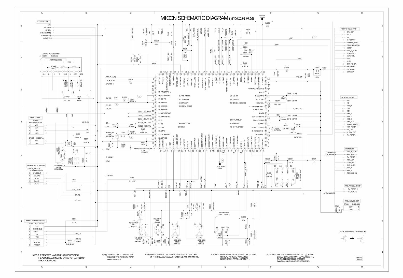
A B C D E F G H
A B C D E F G H
2
1
3
4
5
6
7
8
2
1
3
4
5
6
7
8
D100
4RD
12FB
D101
4
MTZ
J5.1
B
D100
511
E1-E
IC
D1002
1SS133
D1001
11E1-EIC
Q1024DTC143EKA
LED DRIVER
Q1004DTC124EKA
FF/REW_SW
CP1005_1IMSA-9604S-05Z14
1
2
3
4
5
IC10
99S-
24C0
4BDP
-LA
EEP
ROM
1234
5 6 7 8
IC1002 PST600HSYSTEM RESET
1 2 3
R1005
2.7 1W
D100
3SI
D105
0CM
Q1003GP1S94L
MS_SEN B
1
2 3
4
Q1009GP1S94L
MS_SEN A
1
2 3
4
SW10
01SP
VF13
0100
TAB
SW
123 4
IC1003 BA6955NLOADING MOTOR DRIVER
1 2 3 4 5 6 7 8
CP1004 TMC-J08P-B1
1
2
3
4
5
6
7
8
DANS LA NOMENCLATURE DES PIECESN’UTILISER QUE CELLS DECRITESDANGEREUSES AN POINT DE VUE SECURITE
ETANTLES PIECES REPAREES PAR UNATTENTION:
DESCRIBED IN PARTS LIST ONLYCRITICAL FOR SAFETY,USE ONES
ARESINCE THESE PARTS MARKED BYCAUTION:
Q1005RPI-301
REEL SENS
1 2
34
Q1001RPI-301
REEL SENS
1 2
34
L10012.2uH
Q10022SC2412K
SENSOR SW
X100112MHz
X100232.768KHz
C102
1
3316
VKA
C100
3_1
1000
6.3V
YK
C105
8
100
6.3V
KA
C1020
1016V KA
C100
1
100
25V
YK
C101
4
0.1
F
C1030
0.1 B
C106
8
0.1
B
C104
4
0.01
B
C102
8
0.1
B
C1048 18P CH
C1040 18P CH
C1047 18P CH
C1046 20P CH
C103
8
680P
CH
C106
5
0.1
F
C1066
0.1 B
C1034
0.1 F
C1031
0.001 B
C1035
200P CH
C10130.0039 B
C100
6
100P
CH
C107
1
100P
CH
C102
9
0.01
B
C1002
0.001 B
C1039
68P CH
C101
7
0.1
B
C1005
0.001 B
C106
3
0.1
F
C1062
1 B
C10260.1 B
C106
115
0PCH
C106
015
0PCH
C102
322
0PCH
C101
022
0PCH
C100
922
0PCH
C103
739
0PCH
C105
122
0PCH
C1041
0.1 B
C1050
20P CH
C1049
22P CH
C1033
68P CHC1
008
100P
CH
C102
5
0.1
B
C1022
0.1 B
C10270.0039 B
C10190.001 CH
R1078
390KR103
4
560K
R101
6
270
1/4W
R1049
4.7K
R1004
1K
R1040
33K 1/4W
R1024
1K 1/4W
R1029
4.7K
R103
1
1K
R1008
1K
R105
1
5.6K
R107
9
221/
4WR1
083
56K
R108
7
56K
R105
0
100
R106
6
1K
R1044
3.3K
R102
8
4.7K
1/4W
R1032
10K
R1033
1K
R1077
1K
R100
6
47K
R101
1
47K
R100
3
82K
R101
8
4.7K
R101
733
K
R102
022
K
R104
53.
3K
R103
9
18K
1/4W
R1010
3.3K 1/4W
R105
3
220
R103
63.
3K
R100
722
0
R102
122
0
R103
522
0
R100
13.
3K1/
4W
R104
6
4.7K
1/4W
R104
7
4.7K
1/4W
R100
2
120
1/4W
R101
9
47K
R1025560KR1054
150K
R101210K
R1009 560 1/4W
R1013 560 1/4W
C103
2
220
6.3V
KA
C1015 4710V KA
C1016 2216V KA
C1018 4.750V KA
W849
W867
W824
W851
W808
W869
TP1001SERVICE
TP1002VIDEO.H.SW
CAUTION: DIGITAL TRANSISTOR
DURING PLAYBACKMEASURED WITH THE DIGITAL TESTER
NOTE: THE DC VOLTAGE AT EACH PART WASOF PRINTING AND SUBJECT TO CHANGE WITHOUT NOTICE
NOTE:THIS SCHEMATIC DIAGRAM IS THE LATEST AT THE TIME
IC1001OEC7043B
TIMER SYSCON SERVO MICON 1 10
100
11 12 13 14 15 16 17 18 192 20 21 22 23 24 25 26 27 28 293 30
3132
3334
3536
3738
39
4
4041
4243
4445
4647
4849
5
50
515253545556575859
6
60616263646566676869
7
70717273747576777879
8
80
8182
8384
8586
8788
89
9
9091
9293
9495
9697
9899
CP1006IMSA-9604S-04Z14
1
2
3
4
CP1002 CH22076A
1
2
CP1001 52287-0211
1
2
IS NON POLAR ONE.THE ALUMI ELECTROLYTIC CAPACITOR MARKED NPTHE RESISTOR MARKED F IS FUSE RESISTOR.NOTE:
GND
P.CON+5V
AT+12V SDA
SCL
OSD_
R
OSD_
G
OSD_
B
CAP_
CTL
REEL
_T
REEL
_S
CENT
LED
OSD_
BLK
ENV_DET
CYL_
DRIV
E
DOC_
XO_C
TL
REC/
EE/P
B
AT+5V[BACKUP]
EXT_
A_M
UTE
V.RE
C_ST
_H
POW
ER_F
AIL[
DC]
CTL+
TRIC
K_PB
-H/E
E-H
AT+5V[UCON]CTL-MOTOR_GNDC_ROTARY
DUMMY_V.SYNC
TRICK_PB-H/EE-H
COMP
VCR_A_MUTE
V.REC_ST_H
INPUT_SEL
SYNCSYNC
H.SW
DOC_XO_CTL
REC/EE/PB
SD_VIDEO
SP/LP/EP-H
VCR_A_MUTE TAB_SW
TV_A_MUTE
SP/LP/EP-H
LM-
LM+
CAP_FGHD
VD
AFT_MCYL_FG
SCLCYL_PG X_RAY_TEST
LDM
_F
LDM
_R
SDA
OSD_R
EOT
BOT
OSD_G
OSD_B
OSD_BLKCENTLED CTL-POWER_FAIL[DC]
VCR_POWER_HCTL+
IIC_OFFLM-
X_RAY_TESTLM+RESET
TV_POWER_HINPUT_SEL
DEW
VCR_A_MUTETV_POWER_HTAB_SWEXT_A_MUTEVCR_POWER_H
TV_POWER_HC_ROTARY
REC_LEDH.SW
T-REC_LED
EXT_MUTE
KEY_A
KEY_B
REMOCON_INCAP_F/R
DUM
MY_
V.SY
NC
REM
OCON
_IN
MS_
SEN-
A
MS_
SEN-
B
EXT_
MUT
E
T-RE
C_LE
D
ENV_
DET
SEN_
LED
IIC_O
FF
REC_
LED
AFT_
M
KEY_
A
KEY_
B
LDM
_R
LDM
_F
COM
P
EOT
BOT
SCL
SDA
TV_POWER_HCYL_DRIVETV_A_MUTE
RESE
T
REEL
_T
REEL
_S
SEN_
LED
AT+5V[BACKUP]
MS_
SEN-
B
MS_
SEN-
A
CYL_FG
CYL_PG
DEW
CAP_CTL
CAP_FG
CAP_F/R
FROM/TO CHROMA
PCB010VMX195
FROM/TO I/O
FROM/TO Y/C/A/H.AMP
FROM/TO CAPSTAN DD UNIT
FROM/TO MICRO MOTOR
FROM/TO DECK
FROM/TO POWER
(CD1003)
(SYSCON PCB)MICON SCHEMATIC DIAGRAM
VCC
EOT
0
5.10
00 0
0
SDA
SCL
TEST VC
CA0A1A2VS
S
0
2.5 2.6 5.2
0
5.2
5.2
0
0
0
0
1.5
1.3
2.1
2.6
0
5.2
2.5
2.6
5.2
5.21.62.31.8
0
5.1
5.9
2.5
2.0
0.6
2.5
2.5
0.2
0
2.5
2.6
2.5
5.1
5.2
0
1.40.8
0
012.1 00 10.8 0 10.9 12.1
POWERSAVE
CONTROL LOGICSTD
1.4
5.20.8
0.5
5.11.3
1.2 5.2
0 0.9
NC
5.25.1 0
GND OUTIN
0 1.2
NC
NC
10 K
EY B
19 H
I-FI-H
.SW
18 V
IDEO
-H.S
W
99 ANALOG VCC
58 H
/C-S
YNC
59 V
-SYN
C
57 N
UA
55 V
HOLD
53 O
SD-V
CC
52 S
D-IN
(MON
I)
16 H
EAD.
AMP.
SW
15 C
OLOR
ROT
ARY
13 D
UMM
Y-V.
SYNC
12 C
AP-L
IMIT
11 C
AP-F
WD
72 II
C-DA
TA1
71 II
C-CL
K1
74 J
UST
CLOC
K
60 O
SD O
UT1
56 C
VIN
54 H
LF
14 R
EMOC
ON-IN
67 Y
C DO
C/XO
CTL
69 T
RICK
PB-
H
73 F
F/RE
W-L
70 E
XT A
MUT
E
75 T
ONE.
CONT
1 M
SSEN
-A
2 M
SSEN
-B
3 EO
T
4 BO
T
89 DRUM-FG
90 DRUM-PG
93 C
94 CTL-
95 CTL+
96 AMP C
97 CTL AMP-OUT
26 E
XT-M
UTE
28 T
V-PO
WER
27 V
CR-P
OWER
29 T
-REC
LED
30 R
EC L
ED
25 II
C-OF
F
21 L
DM-F
WD
20 L
DM-R
VS
41 X RAY TEST
39 X-OUT(12MHz)
38 X-IN(12MHz)
37 VCC
34 RESET-L
40 VSS
51 S
ERVI
CE
46 NUB
45 OSC-OUT2
44 OSC-IN2
43 CLKSEL
61 R
EC-H
/EE-
M/P
B-L
65 C
AP F
ULL
66 V
-REC
-ST-
H
76 C
AP-P
WM
77 D
RUM
-PW
M
79 R
EEL-
S
80 R
EEL-
T
86 CFG AMP-OUT
87 CAP-FG
88 AMP-VSS
68 C
ENTE
R LE
D
49 OSD-VSS
31 ON-TIMER LED100 DEW
85 POWER-FAIL-L
36 XC-OUT(32KHz)
35 XC-IN(32KHz)
42 CS-EASY-REC LED
47 CM-ADV-VIDEO/AV1
48 CM-ADV-AUDIO/AV2
17 E
NV-C
MP-
IN
8 AF
T(RE
C)
7 AF
T(M
ONI)
9 KE
Y A
91 AMP-VREF OUT
92 AMP-VREF IN
E/V-
MAS
K/PL
AY L
ED
82 TV-A-MUTE
83 SP/LP/EP-H
81 VCR-A-MUTE 50 TAB SW
5.1
22 D
EGAU
SS-H98 AMP-VCC
33 INPUT-SELCT
64 O
SD R
63 O
SD G
62 O
SD B
84 CM/MA-SELECT
5 HI
-FI-E
NV-D
ET
6 VI
DEO-
ENV-
DET
32 OTPB LED
24 S
P-H
23 M
S SE
NS L
ED
CYL DRIVE
CYL PG
CYL +B
CYL FG
CYL GND
FG
VCO
GND
MOTOR GND
I LIMIT
CTL
CAP.M F/R
VCC(5V)
BOT
LDM-
LDM+
VCC
FROM/TO SOUND AMP
DEW+
DEW-
FROM DEW SENSOR
0
0
0 0 5.1 0 0 4.7 0 4.9 5.22.14.24.95.12.52.62.52.50.90.9
NC
NC
NC
000 0 0 00
0
0
0
5.1
0 0 0 0 0 4.81.4 1.4 0 0 2.4 2.2 5.2 5.2 0 2.2 0 0 0 5.2 2.3 2.6 0 0NC
0 0.1 5.2 5.2 0 0
16
17
18
19
20
22
21
0 0.9
2.41.2
05.1
0

A B C D E F G H
A B C D E F G H
2
1
3
4
5
6
7
8
2
1
3
4
5
6
7
8
THE DC VOLTAGE AT EACH PART WAS MEASURED WITH THE DIGITAL TESTER WHEN THE COLOR BROADCAST
WAS RECEIVED IN GOOD CONDITION AND PICTURE IS NORMAL.
NOTE:
HS1100763SAE0067
L101HF57T18.5*10*10 D1
101
11EQ
S04N
D610
SB10-03A3
D620
11ES1
IC1101 KIA7805PI5V REG
1 2 3
CD810 CH28113A
1
2
3
4
5
6
7
8
DANS LA NOMENCLATURE DES PIECESN’UTILISER QUE CELLS DECRITESDANGEREUSES AN POINT DE VUE SECURITE
ETANTLES PIECES REPAREES PAR UNATTENTION:
DESCRIBED IN PARTS LIST ONLYCRITICAL FOR SAFETY,USE ONES
ARESINCE THESE PARTS MARKED BYCAUTION:
Q11022SC13840W
P.CON SW
Q6112SC13840W
REG.
Q6022SC13840W
REG.
Q6032SC13840W
REG.
Q6062SC13840W
REG.
Q6102SD734
REG.
C110
1
0.1
B
R4080
100
R644
100 1/4WR663
100
R110
2
100
1/4W
C110
2
330
10V
YK
C671
100
16V
YK
C670 22
16V
KA
C652
4.7
25V
KA
C643 22
16V
KA
W84
5
OF PRINTING AND SUBJECT TO CHANGE WITHOUT NOTICENOTE:THIS SCHEMATIC DIAGRAM IS THE LATEST AT THE TIME
AT+1
3V
P.CON+5VGNDP.CON+8V
P.CON+5V[CHROMA]AT+5V[BACKUP]
AT+5V[UCON]
AT+12VP.CON+5V[TU1]
P.CON+5V
MOTOR_GNDAT+5V[UCON]GND
AT+5V[BACKUP]
8.7VREF
5.7VREF[PCON]GND
AT+30V5.7VREF[AT]P.CON+5V[CHROMA]
P.CON+5V[TU1]
P.CON+8V
8.7VREFP.CON+9V5.7VREF[PCON]
5.7VREF[AT]
AT+13V
GNDAT+12V
AT+5V[UCON]MOTOR_GND
P.CON+9V
UNREG+8V
AT+13V
AT+30V UNREG+8V P.CON+5VGND
GND
(SYSCON PCB)
POWER SCHEMATIC DIAGRAM
FROM/TO CHROMA
FROM/TO MICON
FROM TV POWER
PCB010VMX195
(CP502)
5.208.2
IN GND OUT
GND
GND
AT+12V
MOTOR GND
UNREG+8V
UNREG+8V
AT+13V
AT+30V
FROM/TO I/O
NC NC
FROM/TO SOUND AMP
FROM/TO Y/C/A/H.AMP
8.5 4.9
5.5
8.7 4.9
5.5
8.5 5.0
5.5
8.6 5.0
5.6
11.7 8.5
9.1
8.9
8.28.7

A B C D E F G H
A B C D E F G H
2
1
3
4
5
6
7
8
2
1
3
4
5
6
7
8
GND
B+
Vout
OS1001GP1U281Q
1
2
3
SW10
02SK
HVBE
D010
REW
/REV
SW10
12SK
HVBE
D010
INPU
T SE
LECT
SW10
03SK
HVBE
D010
FF/C
UE
SW10
04SK
HVBE
D010
VOL
DOW
N
SW10
05SK
HVBE
D010
PLAY
SW10
06SK
HVBE
D010
VOL
UP
SW10
07SK
HVBE
D010
STOP
/EJE
CT
SW10
09SK
HVBE
D010
CH U
P
SW10
08SK
HVBE
D010
REC/
OTR
SW10
10SK
HVBE
D010
CH D
OWN
SW10
11SK
HVBE
D010
POW
ER O
N/OF
F
CC4201 CC4202
H1 H2
E
J4202AV2-20D-2
1
2 3H1 H2
E
J4201AV2-20D-2
REAR A/V JACK(MONO)
1
2 3
S811X
S811YS810X
S810YS802X
S802Y
H NC
E
J1002HTJ-032-05AW
FRONT A/V JACK (MONO)
1
2 3H NC
E
J1001HTJ-032-05AY
1
2 3
D792
SLR-
342V
CT32
POW
ER
D793
SLR-
342V
CT32
REC/
OTR
D791
SLR-
342V
CT32
T-RE
C
D420
6
MTZ
J13B
D420
7
MTZ
J6.8
B
D4201
MTZJ5.6B
D420
8
SB10
-03A
3
D421
0
1SS1
33
D420
9
1SS1
33
Q4204DTC114EKA
TV POWER SWQ4206
DTC114EKA
T-REC LED SWQ4205
DTC114EKA
REC LED SW
L1002
100uH
Q42032SC2412K
AUDIO MUTE
Q42122SA1037AK
BUFFER
Q42102SA1037AK
MUTE SW
C4209
1025V KA
C4211
47016V YK
C421
4
4.7
50V
KA
C420
7
0.1
B
C420
6
0.1
B C420
4
470P
CH
C104
5
0.1
F
C421
2
0.00
1B
C108
7
0.00
1B
C108
4
100P
CH
C108
5
0.00
1B
C421
0
470P
CH
C420
5
470P
CH
R4238
33
R4239
220 1/2W
R4213
75R4
236
1K
R420
3
100
R4244
1K
R761
270
R754
270
R793
270
R1084
5.6K
R1086
2.7K
R1088
1.5K
R1080
33K
R1089
1.5K
R1090
1K
R1095
1K
R420
1
75
R423
2
10K
R1091
1K
R1096
1K
R421
2
75
R4243
2.2K
R4204
1K
C4241
1016V KA
C422
0
100
10V
YK
C100
4
220
6.3V
KA
W85
5
W816
L4205
100uH
TP4201V.OUT
CAUTION: DIGITAL TRANSISTOR
DURING PLAYBACKMEASURED WITH THE DIGITAL TESTER
NOTE: THE DC VOLTAGE AT EACH PART WASOF PRINTING AND SUBJECT TO CHANGE WITHOUT NOTICE
NOTE:THIS SCHEMATIC DIAGRAM IS THE LATEST AT THE TIME
GND
AT+5V[UCON]
REC_LED P.CON+9V
T-REC_LED
KEY_B
KEY_A
REMOCON_IN
TV_POWER_H
EXT_MUTE
VCR_A_MUTE
EXT_A_MUTE
FRONT_AUDIO
FRONT_VIDEO
CHROMA_VIDEO
REAR_AUDIO
REAR_VIDEO
Y/C_AUDIO
23
FROM/TO Y/C/A/H.AMP
FROM/TO MICON
PCB010VMX195
0
0
4.50
0
3.63.6
0
0
3.5
2.5
0
1.90
0
FROM/TO POWER
24
8.5
9.2
9.2
I/O SCHEMATIC DIAGRAM(SYSCON PCB)

A B C D E F G H
A B C D E F G H
2
1
3
4
5
6
7
8
2
1
3
4
5
6
7
8TU
601
TECC
1040
PG32
A
1
10
11
1213
1415
2
3
4
5
6
7
8
9
OUTOUTGININ
CF601SAF45MFY220ZR
SAW FILTER
1 2 3 4 5
CF60
3EF
CT4R
5YS5
A
CF604EFCT4R5MW5
CP601 CH2B026A
1
10
11
2
3
4
5
6
7
8
9
CP6028283_0712_00_000
1
2
3
4
5
6
7
IC601M61203CFP
CHROMA
1 10 11 12 13 14 15 16
1718
19
2
2021
2223
2425
2627
2829
3
3031
32
33343536373839
4
404142434445464748
495
5051
5253
5455
5657
5859
660
6162
6364
7 8 9
B602
BL02RN1-R62
THE DC VOLTAGE AT EACH PART WAS MEASURED WITH THE DIGITAL TESTER WHEN THE COLOR BROADCAST
WAS RECEIVED IN GOOD CONDITION AND PICTURE IS NORMAL.
NOTE:
HS601763WAA0014
L102HF57T18.5*10*10
D609 MTZJ6.8B
D612 MTZJ6.8B
D614
MTZ
J6.8
B
D615
MTZ
J6.8
B
D613
MTZ
J6.8
B
D611
MTZJ9.1B
D608
MTZ
J6.8
B
D619
MTZ
J6.8
B
D602 MTZJ8.2C
D605
11ES1N
D601 1SS133
D607
1SS133
D616
1SS133D617
1SS133D618
1SS133
CD850 CH25095A
1
2
3
4
5
DANS LA NOMENCLATURE DES PIECESN’UTILISER QUE CELLS DECRITESDANGEREUSES AN POINT DE VUE SECURITE
ETANTLES PIECES REPAREES PAR UNATTENTION:
DESCRIBED IN PARTS LIST ONLYCRITICAL FOR SAFETY,USE ONES
ARESINCE THESE PARTS MARKED BYCAUTION:
L601
_1
1.2u
H
L607
18uH
L614100uH
Q6012SA1037AK
BUFFER
X602
100CT3R5053.579545MHz
C607
0.1
B
C613
0.1 B
C602
0.1 F
C664 1 TF
C6570.022 B
C661
0.01 B
C653
0.01
B
C614
0.01
B
C658
0.22 B
C640
0.1
B
C625
1 F
C650
0.01
5B
C623
0.0047 B
C618 100P CH
C6271 B
C615
0.001 CH
C605
100P
CH
C604
100P
CH
C636
0.01
B
C667
0.047 B
C642
100P CH
C663390P CH
C628
220P
CH C654
18P
CH
C660
0.1
B
C666
100P CH
C647
0.01
B
C639
0.01
B
C637
0.01
B
C616
0.01
B
C634
0.01
B
C621
0.01 B
C622
0.1 B
C626
0.1 BC6
73
0.1
TF
C609
0.01
B
C630 0.01 B
C631 1 F
R632
10K
R674
1.8K 1/4W
R673 2.2K
R643
47KR648
2.2K
R647
2.2K
R60810K
R618 10M
R638
150K 1/4W
R609 680
R607
82 1/2W
R633
8.2K
R601
2.2K 1/4W
R651
470R650
560
R616
220
R620
100
R662
1.5K
R622
220
R672
470
R625
10K
1/4W
R642
10K
R646
100K
R623
4.7K
R636
100
R634
100
R630
100
R655
100
R635
100
R660
1.5K
R659
1.5K
R658
1.5K
R631
8.2KR6
57 1K
R626
10K
R656
2.2K
R624
2K
R621 1K
R614 390K
R610
100 1/4W
R603
220
R602
220
R605
220K
R611 10K
C612
2206.3V YK
C601
150V KA
C648_1
150V KA
C641
470
25V
YK
C649 1
50V
KA
C645 1
50V
KA
C620 47
6.3V
KAC659
4716V KA
C655 47
16V
KA
C635 47
16V
KA
C610
2.2
50V
KA
C6322.250V KA
C624
4716V KA
W81
9
W84
4
W80
7
W83
3
W841
W809
W835
W853
W804
W813
W80
3W81
8
W801
W852
W850
L603
100u
H
L608
100uH
OF PRINTING AND SUBJECT TO CHANGE WITHOUT NOTICENOTE:THIS SCHEMATIC DIAGRAM IS THE LATEST AT THE TIME
C665_1
1016V NP
IS NON POLAR ONE.THE ALUMI ELECTROLYTIC CAPACITOR MARKED NPTHE RESISTOR MARKED F IS FUSE RESISTOR.NOTE:
8.7V
REF
POWER_FAIL[DC]
5.7V
REF[
AT]
5.7V
REF[
PCON
]
VD
OSD_R
OSD_G
OSD_B
OSD_BLK
SDA
SCL
AFT_M
VCR_POWER_H TU_VIDEO
HD
X_RAY_TEST
TV_POWER_H
IIC_OFFCHROMA_VIDEO
Y/C_AUDIO
TU_AUDIOB.OUT
TU_VIDEOAGC_M
CHROMA_VIDEO
SOUND+BAUDIO_OUT
SOUND_GND
AUDIO_OUT
Y/C_AUDIO VD
AGC_M
OSD_BLK SOUND+B
SOUND_GND
H_OUT
V_FEEDBACK
V_OUT
ACL
H_PLUSE
TV_POWER_HTU_AUDIOPOWER_FAIL[DC]
AFT_M X_RAY_TEST
AGC_M
V_OUT
OSD_R
OSD_G
OSD_B
HD
G.OUTAT+30V
R.OUTGND
B.OUTP.CON+5V[TU1]
AT+13V
P.CON+5V[CHROMA]
P.CON+8V
8.7VREF
5.7VREF[PCON]
5.7VREF[AT]VC
R_PO
WER
_H
H_PL
USE
H_OU
T
R.OU
T
G.OU
T
B.OU
T
SCL
SDA
PCB010VMX195
FROM/TO POWER
TEST POINT
FROM/TO MICON
(SYSCON PCB)CHROMA SCHEMATIC DIAGRAM
(CP850)
(CP820)
G IN
H PLUSE
NC
TO CRT
FBP
IN
SCL
RF AGC OUT
AFT OUT
VIF GND
VIF VIDEO OUT
QIF IN
VIF APC FILTER
VIF VCO F/B
AUDIO BYPASS
EXT AUDIO IN
FM DIRECT OUT
R OU
T
AFC
FILT
ER
DEF
H OU
T
SDA
H VC
O F/
B
POW
ER O
N CO
NT
B IN
V RAMP FEEDBACK
V RAMP CAP
V PULSE OUT
R IN
CHRO
MA
APC
FILT
ER
TV/Y
IN
Y SW
OUT
VIDE
O/CH
ROM
A GN
D
FAST BLK
SPOT KILLER
G OU
T
RF AGC FILTER
INTE
LLIG
ENT
MON
I
MCU
RES
ET
5.7V
REG
OUT
(FOR
CPU
)
47 LIMITER IN48 IF AGC
64 VIF IN
H.PL
USE
OUT
NC
NCNC
IF
+30V
SDA
SCL
AGC
+5V
NCNC
1.8
2.5
4.9
0
2.5
2.5
29.3
GND
GND
V.FEEDBACK
V.OUT
ACL
SOUND GND
X-RAY TEST
POWER FAIL(DC)
IIC_OFF
SCL
AGC_M
B.OUT
SDA
INTELLGENT MONI
NC
SW R
EG C
ONT
AUDIO OUT
VREG VCC
5V R
EG
VIF
VCC
VIF
IN
B OU
T
EXT
C INQIF OUT
8.7V
REG
OUT
32 X’TAL
31 ACL/ABCL
17 V OUT
FSC OUT
VIDEO CHROMA VCC
STRAT UP VCC
HI V
CC
0 0
2.3
2.4
2.3
3.0
2.0
3.2
9.0
3.0
2.2
0
0
2.4
2.9
2.3
2.7
1.5
1.5 5.0 5.0 2.6 3.6 0.8 2.5 3.93.6 3.4 4.8 2.5 2.5 2.4
3.8
8.5
2.0 2.0 8.2 8.2 8.2 4.0 4.8 5.5 2.8 5.6 0 0 3.2 3.2 2.0 8.8
3.3
3.0
0
4.7
0
0.1
7.3
5.0NC
4.9
4.9
4.8
2.0
0
8.5
SOUND+B
H.OUT
TV POWER H
FROM/TO DEFLECTION
FROM/TO SOUND AMP
FROM/TO Y/C/A/H.AMP
25
3.4
0
2.7
B.OUT
R.OUT
G.OUT
GND
CUT OFF

A B C D E F G H
A B C D E F G H
2
1
3
4
5
6
7
8
2
1
3
4
5
6
7
8
SPEAKER
SP351C908-8-03A
8 OHM
2
1
CD351CH12444A
J351HSJ2000-01-010
HEADPHONE JACK
1
2
3
4
5
6
7
B302
BL01
RN1-
A63
B303
BL01RN1-A63B301
BL01RN1-A63
CC001
THE DC VOLTAGE AT EACH PART WAS MEASURED WITH THE DIGITAL TESTER WHEN THE COLOR BROADCAST
WAS RECEIVED IN GOOD CONDITION AND PICTURE IS NORMAL.
NOTE:
HS351763WSA0009
IC35
1AN
7511
SOUN
D AM
P
1234
5 6 7 8
DANS LA NOMENCLATURE DES PIECESN’UTILISER QUE CELLS DECRITESDANGEREUSES AN POINT DE VUE SECURITE
ETANTLES PIECES REPAREES PAR UNATTENTION:
DESCRIBED IN PARTS LIST ONLYCRITICAL FOR SAFETY,USE ONES
ARESINCE THESE PARTS MARKED BYCAUTION:
C354
_2
3300
16V
YK
C351 2.2
50V
KA
C360
0.018 B
R352
4.7K
R359
47K
R301
56 1/2W
R353
68K 1/4W
R351
5.6K 1/4W
R360
56 1/2W
C356 10
16V
KA
C355
1016V KA
C3573.350V KA
C3583.350V KA
W85
6W832
W837
W821
(W144)
W847
W846
W831
OF PRINTING AND SUBJECT TO CHANGE WITHOUT NOTICENOTE:THIS SCHEMATIC DIAGRAM IS THE LATEST AT THE TIME
CP353 B2B-EH-A
1
2
C362
4716V KANP
IS NON POLAR ONE.THE ALUMI ELECTROLYTIC CAPACITOR MARKED NPTHE RESISTOR MARKED F IS FUSE RESISTOR.NOTE:
SOUND_GND
SOUND+B
AUDIO_OUT
TV_A_MUTE
TV_POWER_H
GND
FROM/TO CHROMA
PCB010VMX195
FROM/TO POWER
SOUND AMP SCHEMATIC DIAGRAM
(SYSCON PCB)
26
FROM/TO MICON
-+
0
08.2 3.5 3.4
3.95.1 0.3
SP OUT +
SP OUT -
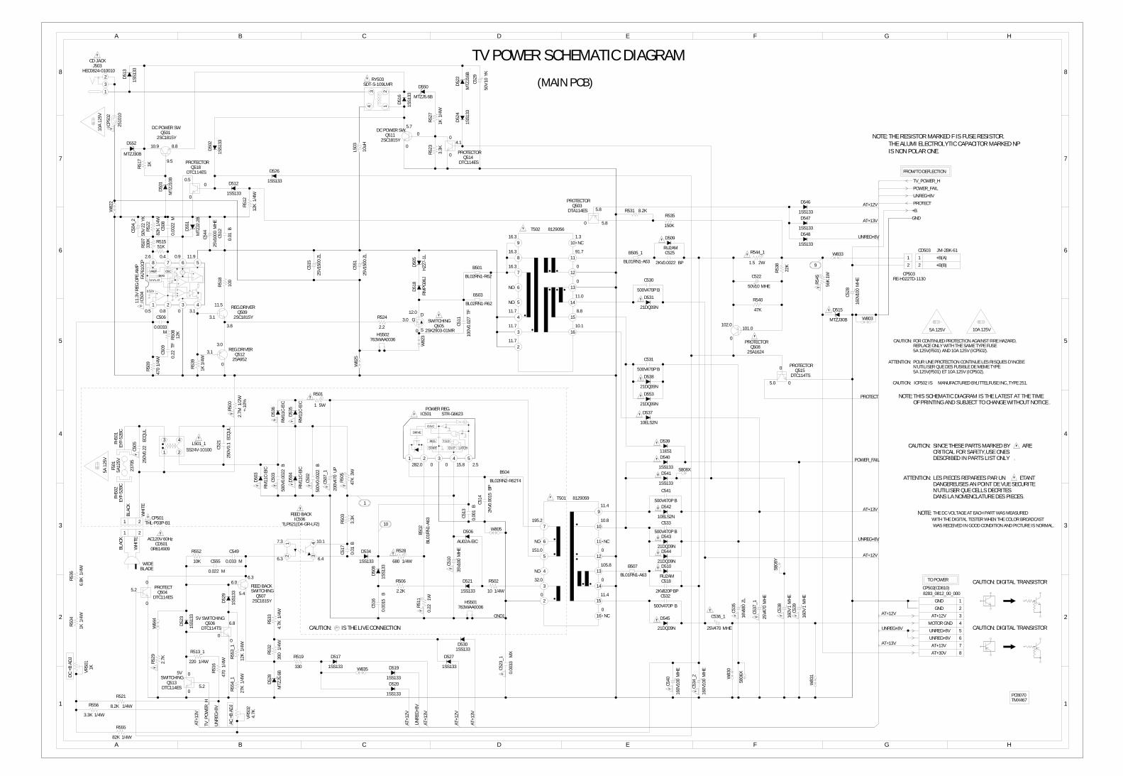
A B C D E F G H
A B C D E F G H
2
1
3
4
5
6
7
8
2
1
3
4
5
6
7
8
R540
47K
R538
22K
R535
150K
R506
2.2K
R519
330
R533
4.7K
1/4W
R552
10K
R553
_1
12K
1/4W
R554
_1
27K
1/4W
R516
470
1/4W
R513_1
220 1/4WR529
2.7K
R503
3.3K
R524
2.2
R512
12K
1/4W
R523
3.3K
R532
390
1/4W
R507
330K
R518
100
R539
1K1/
4W
R51551K
R531 8.2K
R517
1K
R508
12K
R522
82K
1/4W
R527
1K1/
4W
R509
470
1/4W
R502
10 1/4W
R500
2.7M
1/2W
+-10
%
R536
6.8K
1/4W
R504
1K1/
4W
R555
82K 1/4W
R521
8.2K 1/4WR556
3.3K 1/4W
Q503DTA114ES
PROTECTOR
Q5122SA952
REG.DRIVER
W83
0W835
W84
4
W833
W82
3
W82
2
W805
W83
1
W803
W82
5
Q5072SC1815Y
FEED BACKSWITCHING
Q5112SC1815Y
DC POWER SW.
Q5092SC1815Y
REG.DRIVER
Q5012SC1815Y
DC POWER SW
C536_1
47025V MHE
C529
1050
VYK
C537
_1
470
25V
MHE
C538 1
160V
MHE
C539 1
160V
MHE
C535
680
16V
ZL
C522
1050V MHE
C510
100
35V
MHE
C544
1000
25V
MHE
C504
_2
2250
VYK
C534
_2
100
160V
MHE
C540
100
160V
MHE
C528
100
160V
MHE
C531
470P500V BC5
16
0.00
15B
C523
_1
0.00
33M
X
C555
0.022 M
C549
0.033 M
C517
0.01
B
C502
0.00
2250
0VB
C503
0.00
2250
0VB
C521
0.1
250V
ECQU
L
C505
0.22
250V
ECQU
L
C518
820P2KV BP
C525
0.00222KV BP
C506
0.0033M
C512
0.01
BC508
0.00
22M
C509
0.22
TF
C511
0.02
710
0VTF
C541
470P500V B
C533
470P500V B
C532
470P500V B
C513
0.00
1B
C514
0.00
152K
VBP
C530
470P500V B
C507
_1
470
200V
UP
C515
1500
25V
ZL
C551
1500
25V
ZL
L503
10uH
D545
21DQ09N
D519
1SS133
D529
1SS1
33
D523
1SS1
33
D504
RM11
C-EI
C
D535
RM11
C-EI
C
D503
RM11
C-EI
C
D536
RM11
C-EI
C
D502
1SS1
33
D526
1SS133D512
1SS133
D506
AU02A-EIC
D534
1SS133D510
RU2AM
D509
RU2AM
D513
1SS1
33
D524
1SS1
33
D508
1SS1
33
D520
1SS133
D517
1SS133
D546
1SS133D547
1SS133D548
1SS133
D537
10ELS2N
D553
21DQ09N
D538
21DQ09N
D541
1SS133
D540
1SS133
D539
11ES1
D542
10ELS2N
D544
21DQ09N
D543
21DQ09N
D531
21DQ09N
D5301SS133
D527
1SS133
CP5028283_0812_00_000
1
2
3
4
5
6
7
8
IC50
4FA
7610
CP11
.3V
REG.
OPE
AMP
1 2 3 4
5678
IC506TLP621(D4-GR-LF2)
FEED BACK
12 3
4
D528
MTZ
J5.6
B
D552
MTZJ30B
D515
MTZJ30B
Q515DTC114TS
PROTECTOR
Q504DTC114ES
PROTECT
Q506DTC114TS
5V SWITCHING
Q518DTC114ES
PROTECTORQ514
DTC114ES
PROTECTOR
Q513DTC114ES
5VSWITCHING
DESCRIBED IN PARTS LIST ONLYCRITICAL FOR SAFETY,USE ONES
ARESINCE THESE PARTS MARKED BYCAUTION:
DANS LA NOMENCLATURE DES PIECESN’UTILISER QUE CELLS DECRITESDANGEREUSES AN POINT DE VUE SECURITE
ETANTLES PIECES REPAREES PAR UNATTENTION:
OF PRINTING AND SUBJECT TO CHANGE WITHOUT NOTICENOTE:THIS SCHEMATIC DIAGRAM IS THE LATEST AT THE TIME
CAUTION: DIGITAL TRANSISTOR
CAUTION: DIGITAL TRANSISTOR
5A 125V
5A 1
25V
D505
HZ27
-1L
D550
MTZJ5.6B
D551
MTZ
J2.2
B
D501
MTZ
J10B
D522
MTZ
J16B
J503HEC0824-010010
CD JACK
1
2
3
D518
RMPG
06J
D516
1SS1
33
D521
1SS133
B507
BL01RN1-A63
B502
BL01
RN1-
A63
B504
BL02RN2-R62T4
B503
BL02RN1-R62
B505_1
BL01RN1-A63B501
BL02RN1-R62
IC501 STR-G6623POWER REG.
1 2 3 4 5
HS502763WAA0036
HS501763WAA0006R5
11
0.22
1W
R505
47K
3W
R544_1
1.5 2W
R545
56K
1W
RY503SDT-S-109LMR
123
4
VR50
24.
7K
AC +
B AD
J
VR50
11K
DC +
B AD
J
ICP5
02
2510
10
IS THE LIVE CONNECTIONCAUTION:
R501
1 5W
F501
5A12
5V
2370
5
FH50
1EY
F-52
BCFH
502
EYF-
52BC
L501_1SS24V-101001 2
3 4
CP501THL-P03P-B11 2
R528
680 1/4W
CP503RE-H022TD-1130
1
2
Q5082SA1624
PROTECTOR
S
DG
Q5052SK2903-01MR
SWITCHING
BLADEWIDE
BLAC
K
WHI
TE
21
CD5010R614909
AC120V 60Hz
T502 8129056
10
11
12
13
14
15
16
2
3
4
5
6
7
8
9
T501 8129059
10
11
12
13
14
15
16
2
3
4
5
6
7
9
2
1
CD503 JM-2BK-61
S808X
S808
Y
S806
X
REPLACE ONLY WITH THE SAME TYPE FUSE
N’UTILISER QUE DES FUSIBLE DE MEME TYPE
CAUTION:
ATTENTION: POUR UNE PROTECTION CONTINUE LES RISQUES D’INCEIE
FOR CONTINUED PROTECTION AGAINST FIRE HAZARD,
THE DC VOLTAGE AT EACH PART WAS MEASURED WITH THE DIGITAL TESTER WHEN THE COLOR BROADCAST
WAS RECEIVED IN GOOD CONDITION AND PICTURE IS NORMAL.
NOTE:
IS NON POLAR ONE.THE ALUMI ELECTROLYTIC CAPACITOR MARKED NPTHE RESISTOR MARKED F IS FUSE RESISTOR.NOTE:
TV_POWER_H
POWER_FAIL
UNREG+8V
PROTECTAT+12V+B
GNDAT+13V
UNREG+8V
PROTECT
POWER_FAIL
AT+13V
UNREG+8V
AT+12V
AT+12VGND1
UNREG+8V
AT+13V
TV_P
OWER
_H
UNRE
G+8V
UNRE
G+8V
AT+1
3V
AT+1
2V
AT+1
3V
AT+1
2V
AT+1
3V
PCB070TMX467
FROM/TO DEFLECTION
TO POWER
TV POWER SCHEMATIC DIAGRAM
(MAIN PCB)
LITTELFUSE INC.,TYPE 251.CAUTION: ICP502 IS MANUFACTURED BY
10A 125V
5A 125V(F501) AND 10A 125V (ICP502).
5A 125V(F501) ET 10A 125V (ICP502).
(CD810)
0
05.0
101.0
10
1
0
0
5.2
6.0
5.4
6.3
0
6.8
0
BLAC
K
5.8
5.80
0.5
0
0
0
04.1
0
5.7
0
+B(B)
+B(A)
9
3.1
NC
REG.
DRIVE
-+O.S.C
T.S.D
-+
2.515.800282.0
START O.V.P LATCH
NC
NC
5.20
0
10A
125V
0.5 0.8 0 3.1
2.6 0.4 0.9 11.9
VREF OSC
U.V.L.OBIAS
++-+
0.52V+-
-+
+-
12.0
3.0
0
16.3
16.3
16.3
11.7
11.7
11.7
1.3
91.7
0
0
8.8
10.1
11.0
NC
NC
195.2
151.0
32.0
0
11.4
10.8
0
105.8
0
11.4
0NC
10.9 8.8
9.5
6.4
10.17.3
6.3
102.0
0
WHI
TE
UNREG+8V
UNREG+8V
AT+30V
GND
GND
MOTOR GND
AT+12V
AT+13V
NC
3.1
11.5
3.8
3.0
0

A B C D E F G H
A B C D E F G H
2
1
3
4
5
6
7
8
2
1
3
4
5
6
7
8
R442
12K +-1%
R443
_1
18K
+-1%
R440
_1
8.2K
+-1%
R441
_1
100K
+-1%
R439
_1
27K
+-1%
R404
1.5K +-1%
TP401
K003TMM17538
K001TMM17538
K002TMM17538
BGR
1168
109
175
V801A22JWG098X
DY801KDY3CFB23M
GND GND
ABL
GND
+14V
HEATER
+25V
AFC
B+
+180V
COLHV
F
S
FB401 3210012R
1
10
11
2
3 4
5
6
7
8
9
C
AG
Q402
2P4M
DEGA
USS
DRIV
ER
CP803A51052-0400
1
2
3
4
CP401B04B-DVS
1
2
3
4
T401305Y001
1
2
3 4
6
Q406_12SD2627LS-CBC11
H.OUTPUT
IC401 LA78040V.OUTPUT
1234567
21
L5088R090008
DEGAUSS COIL
CD8032E042705
CD8018M82025A
CP8208283_1112_00_000
1
10
11
2
3
4
5
6
7
8
9
L401
4.7mH 0909
R423
18K 1/4W
R471
10K 1/4W
R401
10K
R411
11K
1/4W R4
14
1.2K
1/4W
R413
12K 1/4W
R416
10K 1/4W
R421
680 1/2W
R419
270
1/2W
R417
470
1/2W
R415
_1
1.5
1/2W
R426
5.6K
R430
27K
R425
220K
1/2W
R456
4.7K
1/2W
R410
1K
R403
2.7K
R420
1.2K
1/2W
R412
10K
1/4W
R424
2.2K
R422
3.9K
R460
100
1/4W
R453
220K 1/4W
R490
47K
1/4W
R472
270K
1/4W
R473
1M 1/4WQ407
DTA114ES
SWITCHING
Q401DTA114ES
DEGAUSE SW
Q4722SA1371
SWITCHING
W827
W813
W818
W842
W877 W875
W83
8
W872W878
W80
1
W816
W824
W812
W83
9
W884
W888
W81
0
W815
W81
9
W88
9
W82
6W
809
Q405_12SC2271
H-DRIVE
Q4082SC1815Y
X_RAY_SW
Q4712SC2909
SWITCHING
C422
_1
125
0VM
HE
C406
_1
100
35V
MHE
C407
1000
25V
YK
C405
_1 3.3
50V M
HE
C403 10
50V
YK
C427
100P500V B
C440
0.00
33M
C416
22P500V SL
C414
4.7
250V
ECQ-
E
C404
0.0022 M C411 0.47
100V
TF
C409
0.01
M
C430
0.00
12K
VBP
C423
0.27
200V
FHS
C438 68
0P50
0VB
C425
_1
0.00
122K
VBP
C424
0.00
681.
6KV
ECW
H
C432 0.1
100V
TF
C417 0.00
150
0VB
C402 22
200V
MHE
C418
_1
116
0VM
HE
C421
_1
470
35V
MHE
C410 1
50V
YK
C433
_1
2210
0VM
HE
D413
RMPG
06J
D402
RMPG
06J
D401
11E1
-EIC
D409
HZ11B3L
D408
HZ27
-1L
Q404DTC114TS
SWITCHING
DESCRIBED IN PARTS LIST ONLYCRITICAL FOR SAFETY,USE ONES
ARESINCE THESE PARTS MARKED BYCAUTION:
DANS LA NOMENCLATURE DES PIECESN’UTILISER QUE CELLS DECRITESDANGEREUSES AN POINT DE VUE SECURITE
ETANTLES PIECES REPAREES PAR UNATTENTION:OF PRINTING AND SUBJECT TO CHANGE WITHOUT NOTICE
NOTE:THIS SCHEMATIC DIAGRAM IS THE LATEST AT THE TIME
CAUTION: DIGITAL TRANSISTOR
CAUTION: DIGITAL TRANSISTOR
D412
RMPG06J
D411
RMPG06J
HS402763WSA0004
HS401763WAS0004
R547
6.8 3W
R449
6.8K
7W
R450
_210
2W
R447
681/
2W
CP403TV-50P-02-A1
1
2
S806
Y
THE DC VOLTAGE AT EACH PART WAS MEASURED WITH THE DIGITAL TESTER WHEN THE COLOR BROADCAST
WAS RECEIVED IN GOOD CONDITION AND PICTURE IS NORMAL.
NOTE:
IS NON POLAR ONE.THE ALUMI ELECTROLYTIC CAPACITOR MARKED NPTHE RESISTOR MARKED F IS FUSE RESISTOR.NOTE:
CRT+B
GND_A
GND_A
HEATER
UNREG+8V
TV_POWER_H
PROTECT
POWER_FAIL
+B
GND
FROM/TO CHROMA
TO CRT
TO DY
(CP601)
(MIAN PCB)DEFLECTION SCHEMATIC DIAGRAM
HEATER
GND
GND
+B17.6
17.79.9
0
17.6
0
0
262.01.3
0
31.00.5
3
8
4
NC
1.3
031.0
22.3
0.2
FOCUS
SCREEN0.2
0
5.9
V.FEEDBACK
V.OUT
ACL
PCB070
VccGND
THERMAL PROTECTION
AMP-+
PUMP UP
3.7 26.3 12.5 0 2.0 25.9 3.6
3.6 0
3.3
2.0
104.6
101.0
33.8
0
0.6
8.1
3.2
0
22.5K
2
NC
NC
FROM/TO TV POWER
SOUND GND
SOUND+B
H.OUT
GND
POWER FAIL(DC)
TMX467
H PULSE
X-RAY TEST
TV POWER H
101.0
101.0102.0
0
0
0.6
12
TO CRT
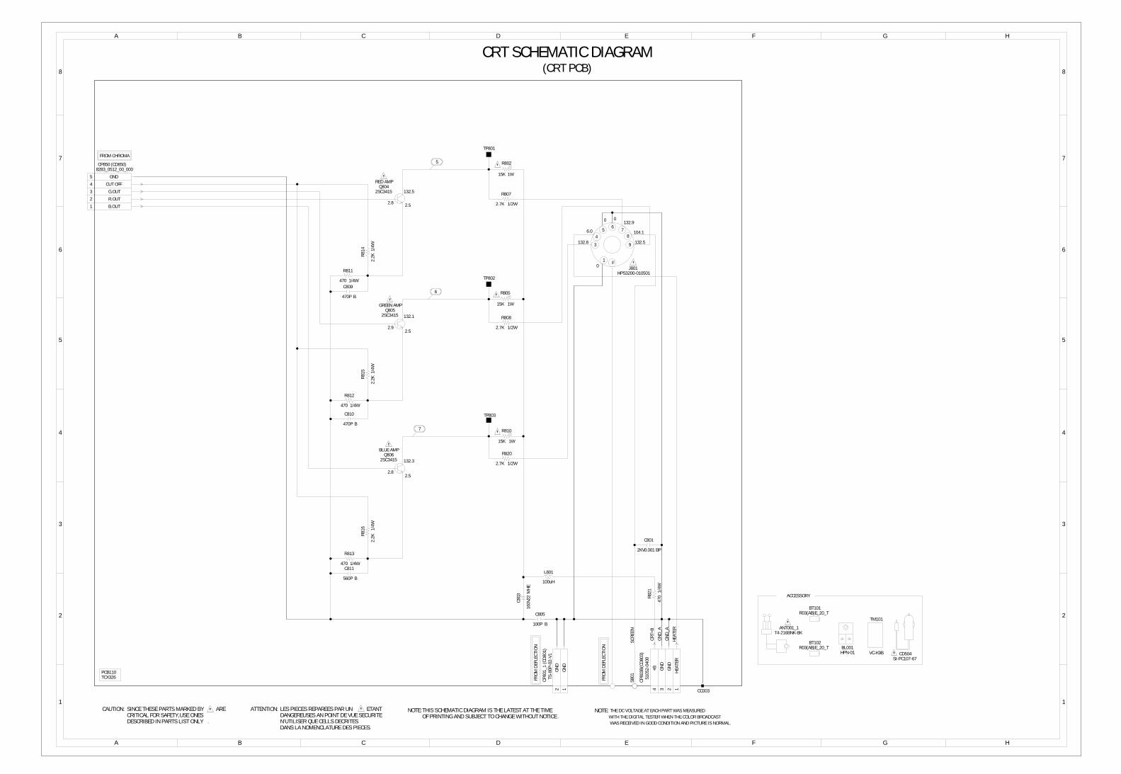
A B C D E F G H
A B C D E F G H
2
1
3
4
5
6
7
8
2
1
3
4
5
6
7
8
CP80
3B51
052-
0400
1234
CP80
1_1
TS-8
0P-0
2-V1
12
CP8508283_0512_00_000
1
2
3
4
5
FJ801
HPS3200-010501
1
3
45
67
8
9
S801
ANT001_1T4-216BNK-BK
TM101
BT102R03(AB)E_20_T
BT101R03(AB)E_20_T
CD504SI-PC107-67
BL001HPN-01
TP803
TP801
TP802
CC003
R808
2.7K 1/2W
R813
470 1/4W
R816
2.2K
1/4W
R812
470 1/4W
R815
2.2K
1/4W
R820
2.7K 1/2W
R807
2.7K 1/2W
R814
2.2K
1/4W
R811
470 1/4W
R821
470
1/4W
Q8062SC3415
BLUE AMP
Q8052SC3415
GREEN AMP
Q8042SC3415
RED AMP
C803 22
160V
MHE
C805
100P B
C811
560P B
C810
470P B
C801
0.0012KV BP
C809
470P B
L801
100uH
DESCRIBED IN PARTS LIST ONLYCRITICAL FOR SAFETY,USE ONES
ARESINCE THESE PARTS MARKED BYCAUTION:
DANS LA NOMENCLATURE DES PIECESN’UTILISER QUE CELLS DECRITESDANGEREUSES AN POINT DE VUE SECURITE
ETANTLES PIECES REPAREES PAR UNATTENTION:OF PRINTING AND SUBJECT TO CHANGE WITHOUT NOTICE
NOTE:THIS SCHEMATIC DIAGRAM IS THE LATEST AT THE TIME
R805
15K 1W
R810
15K 1W
R802
15K 1W
THE DC VOLTAGE AT EACH PART WAS MEASURED WITH THE DIGITAL TESTER WHEN THE COLOR BROADCAST
WAS RECEIVED IN GOOD CONDITION AND PICTURE IS NORMAL.
NOTE:
CRT+
B
GND_
A
GND_
A
HEAT
ER
SCRE
EN
VC-K9B
(CRT PCB)CRT SCHEMATIC DIAGRAM
(CD8
01)
(CD8
03)
(CD850)
GND
GND
FROM
DEF
LECT
ION
ACCESSORY
6
132.3
2.52.8
7
2.52.9
132.1
132.5
2.52.8
5
GND
HEAT
ER
FROM
DEF
LECT
ION
+B GND
FROM CHROMA
00
0
132.8
6.0
132.9
104.1
132.5
GND
G.OUT
R.OUT
B.OUT
CUT OFF
PCB110TCX326
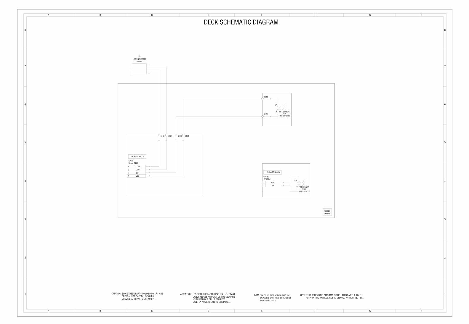
A B C D E F G H
A B C D E F G H
2
1
3
4
5
6
7
8
2
1
3
4
5
6
7
8
Q101RPT-38PB113
BOT SENSOR
Q102RPT-38PB113
EOT SENSOR
DANS LA NOMENCLATURE DES PIECESN’UTILISER QUE CELLS DECRITESDANGEREUSES AN POINT DE VUE SECURITE
ETANTLES PIECES REPAREES PAR UNATTENTION:
DESCRIBED IN PARTS LIST ONLYCRITICAL FOR SAFETY,USE ONES
ARESINCE THESE PARTS MARKED BYCAUTION:
CP10152044-0445
1
2
3
4
CP102173979-2
1
2
S105
S106
S103 S104S101 S102
DURING PLAYBACKMEASURED WITH THE DIGITAL TESTER
NOTE: THE DC VOLTAGE AT EACH PART WASOF PRINTING AND SUBJECT TO CHANGE WITHOUT NOTICE
NOTE:THIS SCHEMATIC DIAGRAM IS THE LATEST AT THE TIME
VE8851
FROM/TO MICON
FROM/TO MICON
M101LOADING MOTOR
DECK SCHEMATIC DIAGRAM
VCC
BOT
LDM-
LDM+
5.1
0
PCB550
VCCEOT
5.1
0

A B C D E F G H
A B C D E F G H
2
1
3
4
5
6
7
8
2
1
3
4
5
6
7
8
H NC
E
J1001FRONT A/V JACK (MONO)
1
2 3H NC
E
J1002FRONT A/V JACK (MONO)
1
2 3
GND
B+
Vout
OS1001
1
2
3
CP80
3B
1234
CP80
3A 1234
CP601
1
10
11
2
3
4
5
6
7
8
9
CP820
1
10
11
2
3
4
5
6
7
8
9
J351HEADPHONE JACK
1
2
3
4
5
6
7
J503CD JACK
1
2
3
2
1
CD351
CP80
1
12
BLAD
EW
IDE
BLACK
WHITE
21
CD501AC120V 60Hz
CP403 12
CP401
1 2 3 4
CD810
1
2
3
4
5
6
7
8
CP502
1
2
3
4
5
6
7
8
H1 H2
E
J4201REAR A/V JACK (MONO)
1
2 3H1 H2
E
J4202REAR A/V JACK (MONO)
1
2 3
OF PRINTING AND SUBJECT TO CHANGE WITHOUT NOTICETHE TIMETHIS INTERCONNECTION DIAGRAM IS THE LATEST ATNOTE:
8
7
6
5
4
3
2
1
8
7
6
5
4
3
2
1
4
3
2
1
4
3
2
1
4
3
2
1
CP4001
6
5
4
3
2
1
6
5
4
3
2
1
CP4002
2
1
CP353
2
1
CP1001
2
1
CP4003
5
4
3
2
1
5
4
3
2
1
CP1005
2 1
L508DEGAUSS COIL
CP501
12
SPEAKER
SP3518 OHM
DANS LA NOMENCLATURE DES PIECESN’UTILISER QUE CELLS DECRITESDANGEREUSES AN POINT DE VUE SECURITE
ETANTLES PIECES REPAREES PAR UNATTENTION:
DESCRIBED IN PARTS LIST ONLYCRITICAL FOR SAFETY,USE ONES
ARESINCE THESE PARTS MARKED BYCAUTION:
CD850
1
2
3
4
5
CP85
0
12345
INTERCONNECTION DIAGRAM
POWER FAIL(DC)
TV POWER H
H.PLUSE
ACL
V.OUT
V.FEEDBACK
GND
H.OUT
SOUND GND
SOUND+B
DY801
V801
TCX326
9
8
765
4
3
1 F
TMX467
MAIN PCBPCB070
HEAT
ER
+B
GND
HEAT
ER
+B
COMMAND TRANSMITTERTM101
SP OUT+
SP OUT-
POWER FAIL(DC)
SOUND+B
UNREG+8V
MOTOR GND
AT+30V
AT+13V
UNREG+8V
AT+12V
GNDGND
EOT
VCC
LDM+
LDM-
VCC
BOT
DEW-
DEW+
VMX195
H.PLUSE
H.OUT
MOTOR GND
SP COM
MOTOR GND
CAP.M F/R
GND
FE HEAD (HOT)
FE HEAD (GND) 2
1
H5002FULL ERASE HEAD ASS’Y
FE HEAD (HOT)
FE HEAD (GND)
CP1002
CP1006
DECK PCBPCB550VE8851
M101LOADING MOTOR
LM
CP102
Q102
EOT
VCC2
1
2
1
EOT SENSOR
1
2
Q101CP101 BOT SENSOR
WHITE
RED
VCC
LDM+
LDM-
BOT
FFC
D1100DEW SENS
1
2
HEAD AUDIO CONTROL ASS’YH5001CD4001
AUDIO PB
AUDIO REC
CTL-
CTL+
AE HEAD(-)
AE HEAD(+) AE HEAD(+)
AE HEAD(-)
AE
AUDIO
CONTROLCTL-
CTL+
AUDIO REC
AUDIO PB
FFC
CUT OFF
CUT
OFF
B.OU
T
R.OU
T
GND
G.OU
T
X-RAY TEST
TV POWER H
V.FEEDBACK
SOUND GND
GND
GND
AT+30V
AT+12V
GND
GND
AT+13V
UNREG+8V
UNREG+8V
X-RAY TEST
ACL
V.OUT
GND
SYSCON PCBPCB010
NC
NC
NC
NC
TU601TUNER PACK
IF
+30V
+5V
SDA
SCL
AGCU IN
11
10
1
3
5
6
7
8
9
2
4
G.OUT CD1003
NC
M2001DECK MECHA ASS’Y
CAPSTAN DD UNIT ASS’Y
CYLINDER UNIT ASS ’Y
4
3
2
1
FFC
UN4001
FOCU
S
SCRE
EN
J801CRT SOCKET
S801
FOCUS SCREEN
GND
GND
CD803
H.V
ANOD
E
FB40
1FB
T
CRT PCBPCB110
GND
R.OUT
B.OUT
VCC(5V)
FG
VCO
CTL
I LIMIT
GND
GOVCC
MRFG SENSOR
ROTORMAGNETCOIL
MAINHALLSENSOR
LOGICSWITCH
OUTIN
HALLVCCHALL
CP1004
CYL FG
CYL PG
CYL +B
CYL GND
CYL DRIVE
SP-CH2 (L)
SP-CH1 (R)CH1 HEAD
SP
CH2
MICRO MOTORM2003
FG.PG GND
GND
PG
FG
CYL PG
CYL +B
CYL FG
CYL GND
CYL DRIVE DRIVE CONTROL
VCC
CD801
CRT

REC/PB0.5V 20µs/div
REC/PB
100mV 0.5µs/div
PB
100mV 5ms/div
REC20V 10µs/div
REC/PB
1V 5ms/div
500mV 2µs/div
5.0V 2µs/div
500mV 5ms/div 10V 5ms/div
2.0V 20µs/div
200mV 20µs/div
10V 20µs/div
10V 20µs/div
10V 20µs/div7
8
16
1
2
3
4
5
6
9
10
11
12
13
1420V 2µs/div
The following waveforms were measured at the point of the correspondingballoon number in the schematic diagram.
NOTE:
WAVEFORMS
TV POWER
DEFLECTION
DEFLECTION
TV POWER
CRT MICON
Y/C/AUDIO/HEAD AMP

REC/PB
2V 20µs/div
PB1V 2ms/div
REC/PB
1V 10ms/div
REC/PB
1V 50ns/div
REC/PB
1V 10ms/div
REC/PB
1V 0.5ms/div
17
18
19
22
21
20
23
24
25
26
REC/PB
200mV 20ns/div
REC/PB0.5V 20µs/div
200mV 20µs/div
200mV 2ms/div
The following waveforms were measured at the point of the correspondingballoon number in the schematic diagram.
NOTE:
WAVEFORMS
IN/OUT
CHROMA
SOUND AMP

B
SP351
101116
118
119
120
124
125
127
209
209
209
MECHANICAL EXPLODED VIEW
206
216
203
203
203
203
129201
201
201
201
L508
V801
132
PCB110(CRT PCB)
J801
115
215
215
PCB070(MAIN PCB)
FB401
131 A
208
208
208
208
213
213213
137
213
214
115208
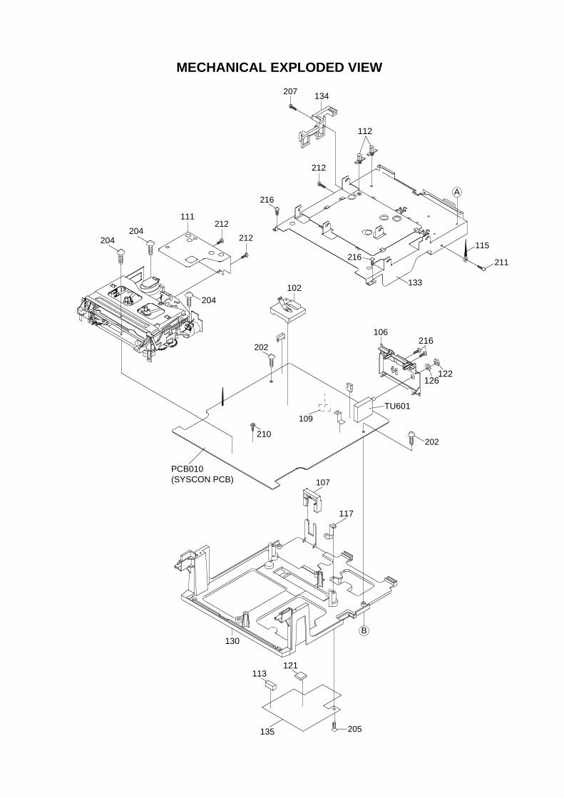
204204
204
111212
212
A216
216115
211
212
112
134207
133
130B
205135
113121
117
107
MECHANICAL EXPLODED VIEW
PCB010(SYSCON PCB)
202
210
TU601
106216
126122
202
109
102

515
360
D1100503
CHASSIS EXPLODED VIEW (TOP VIEW)
321
348
507
H5001
506
305
304301
347
316
313
508
315338
512
310
361
359
368357
366
306366
358
365
351363
323324
362
353
320
335
319
349
318
336
328
512
314
508
313
502H5002
511
509
329
330
502
502
PCB550(DECK PCB ASS'Y)
303
AA
AD
AD
ADAD
AA
AD AD
AA
AA
AB
AB
AD
AD
BA
AA
352
503
503
367
501
356
317369
309
355
300
A
505
334AA
UN4001
M2003
510
M101
364
A
CLASS MARK
GREASE AA
BA
Applying positions AA and BA for the grease or oil are displayed for this section.Check if the correct grease or oil is applied for each position.
NOTE:
OIL

CHASSIS EXPLODED VIEW (BOTTOM VIEW)
AB
302
M2001511
340
514
341
343511
503
345339
342
504
332
346
311
333
346
312
331
514
344
AA
AA
AA
AD
AD
AA
AA
AA
AA
AA
AC
AA
307
354
326
327
322
513
350
308
337
AA
325
AD
AA
AD
300
NOTE: Applying positions AA and BA for the grease or oil are displayed for this section.Check if the correct grease or oil is applied for each position.
CLASS MARK
GREASE AA
BAOIL

MECHANICAL REPLACEMENT PARTS LIST
Location No. TSB P/N Reference No. Description
101 BZ610123 A547A4I720 CABINET,FRONT ASS'Y102 BZ710269 752WSA0213 SHIELD,CASE HEAD AMP ASS'Y106 BZ710280 771WPA0255 PLATE,JACK107 BZ710281 761WPA0203 HOLDER,BUSH109 BZ710282 752WSAA033 SHIELD,IC
111 BZ710283 752WSAA027 SHIELD,COVER DECK112 BZ710284 890PS70100 PUSH SPACER113 BZ710251 800WFA0037 CUSHION 15x5xT=6115 BZ710039 8995034000 CORD CLIP UL CO.116 BZ710285 701WPJ0958 CABINET,FRONT117 BZ710235 753WSA0120 PLATE,BOTTOM-EARTH118 BZ710286 712WPJ0709 FLAP119 BZ710287 713WPA0123 GLASS,LED
120 BZ710288 713WPA0124 GUIDE,REMOCON121 BZ710252 800WFA0038 CUSHION 10x10xT=2122 BZ710038 8300495207 NUT (VOLUME NUT 3/8 INCH)124 BZ710289 738WPA0017 BUTTON,BASE125 BZ710290 735WPJ0164 BUTTON,FRAME126 BZ710037 82A97A4077 WASHER 9.7x14xT0.7127 BZ710010 743WKA0032 SPRING,FLAP129 BZ710291 702WPA0728 CABINET,BACK
130 BZ710292 761WPA0202 HOLDER,DECK131 BZ710293 761WPA0208 HOLDER,FBT132 BZ710294 741WUA0002 SPRING,EARTH133 BZ710295 752WSA0210 PLATE,DECK SHIELD134 BZ710296 761WPA0204 HOLDER,M/PCB135 BZ710248 752WSAA028 SHIELD,BOTTOM137 BZ710324 753KSA0059 SHIELD,TV MAIN PCB
201 BZ710297 8141J40C04 TAPTITE(P) GW14 4x30202 BZ710036 8117540B04 SCREW,TAPPING(B0) TRUSS 4x20203 BZ710035 8117540A64 SCREW,TAPPING(B0) TRUSS 4x16204 BZ710034 8117140A24 SCREW,TAPPING(B0) PAN 4x12205 BZ710158 8110630604 SCREW,TAP TITE(P) BRAZIER 3x6206 BZ710032 8110630A24 SCREW,TAP TITE(P) BRAZIER 3x12207 BZ710240 8107230804 SCREW,TAP TITE(S) BIND 3x8208 BZ710239 8109I30A04 SCREW,TAP TITE(B) WH7 3x10209 BZ710030 8110630804 SCREW,TAP TITE(P) BRAZIER 3x8
210 BZ710028 8110330804 SCREW,TAP TITE(P) FLAT 3x8211 BZ710299 8107230604 SCREW,TAP TITE(S) BIND 3x6212 BZ710017 8107226604 SCREW,TAP TITE(S) BIND 2.6x6213 BZ710019 8109630802 SCREW,TAP TITE(B) BRAZIER 3x8214 BZ710024 810A130B04 SCREW/WASHER(A) M3x20215 BZ710021 810A130604 SCREW/WASHER(A) M3x6216 BZ710031 8110630A04 SCREW,TAP TITE(P) BRAZIER 3x10
--- BZ710300 792WHA0281 PACKAGE,TOP--- BZ710301 792WHA0282 PACKAGE,BOTTOM--- BZ710302 793WCD1266 GIFT BOX--- BZ614143 J547A401 INSTRUCTION BOOK

CHASSIS REPLACEMENT PARTS LIST
Location No. TSB P/N Reference No. Description
300 BZ610090 A547A4B420A DECK ASSY A547A4B420A301 BZ710073 85OA500022 AHC ASS'Y302 BZ710193 85OP200290 BELT,CAPSTAN (S)303 BZ710132 85OP900710 LEVER,REC304 BZ710094 85OP500083 BASE,AC HEAD305 BZ710112 85OP800324 SPRING,AC HEAD306 BZ710194 85OA000367 MAIN CHASSIS ASS'Y (S-Z)307 BZ710195 85OA200082 CLUTCH ASS'Y(S2)308 BZ710196 85OA200080 ARM,IDLER ASS'Y (S)309 BZ710197 85OP600556 ARM,SS BRAKE (S)
310 BZ710198 85OP200292 REEL,T (S)311 BZ710063 85OA300061 LOADING ARM S ASS'Y312 BZ710064 85OA300062 LOADING ARM T ASS'Y313 BZ614076 85OA400210 GUIDE ROLLER ASS'Y314 BZ710069 85OA400188 BASE,INCL S ASS'Y315 BZ710070 85OA400196 BASE,INCL T(S) ASS'Y316 BZ710200 85OA400199 P5-3 ARM ASS'Y(S)317 BZ710072 85OA400205 PINCH ROLLER BLOCK318 BZ710065 85OA400175 TENSION ARM ASS'Y319 BZ710201 85OA400184 TENSION BAND ASS'Y (S)
320 BZ710067 85OA400178 PINCH ROLLER LEVER ASS'Y321 BZ710202 85OA600188 BRAKE T ASS'Y (S):BLACK
BZ710311 85OA600196 BRAKE T ASSY(S):WHITE322 BZ710203 85OA600191 CAP BRAKE ASS'Y(S)323 BZ710076 85OA900213 LINK ASS'Y324 BZ710077 85OA900216 LINK LEVER ASS'Y325 BZ710204 85OP200284 LEVER,CLUTCH (S)326 BZ710205 85OP200285 ACTUATOR,CLUTCH327 BZ710206 85OP200298 GEAR,COUPLING(S2)328 BZ710207 85OP200291 REEL,S (S)329 BZ710096 85OP600541 WORM
330 BZ710105 85OP600563 BRACKET,MOTOR331 BZ710086 85OP300178 GEAR,MAIN LOADING332 BZ710087 85OP300179 GEAR,LOADING S333 BZ710088 85OP300180 GEAR,LOADING T334 BZ710208 85OP300187 HOLDER,LOADING GEAR (S-Z)335 BZ710090 85OP400472 ADJUST,TENSION336 BZ710093 85OP400492 HOLDER,TENSION337 BZ710092 85OP400490 LEVER,TENSION338 BZ710091 85OP400475 COVER,P4339 BZ710097 85OP600543 GEAR,JOINT
340 BZ710098 85OP600544 GEAR,MIDDLE341 BZ710209 85OP600554 CAM,MAIN (S)342 BZ710101 85OP600546 CAM,P5343 BZ710172 85OP600565 CAM,PINCH ROLLER344 BZ710210 85OP600561 ROD,MAIN(S)345 BZ710106 85OP700035 REFLECTOR,LED346 BZ710107 85OP800318 SPRING,LOADING GEAR347 BZ710211 85OP800334 SPRING,P5 (S)348 BZ710212 85OP800335 SPRING,BRAKE T (S)349 BZ710110 85OP800322 SPRING,TENSION
350 BZ710213 85OP800336 SPRING,CAP BRAKE (S)351 BZ710118 85OP800342 SPRING,LOCKER (S)352 BZ710113 85OP800326 SPRING,LINK353 BZ710114 85OP800328 SPRING,DAMPER354 BZ710115 85OP800330 SPRING,RING355 BZ710214 85OP800337 SPRING,SS BRAKE (S)356 BZ710119 85OP900680 OPENER,CASS357 BZ710215 85OP900704 CASS SIDE L:BLACK
BZ710312 85OP900731 CASS SIDE L:WHITE358 BZ710121 85OP900684 CASS SIDE R:BLACK
BZ710313 85OP900732 CASS SIDE R:WHITE359 BZ710131 85OP900709 TAPE GUIDE L (P,R):BLACK
BZ710314 85OP900728 TAPE GUIDE L(P,R):WHITE
360 BZ710122 85OP900686 TAPE GUIDE R:BLACKBZ710315 85OP900729 TAPE GUIDE R:WHITE
361 BZ710130 85OP900707 COVER,SENSOR L362 BZ710123 85OP900688 LEVER,FLAP363 BZ710124 85OP900690 CASS HOLDER364 BZ710095 85OP600540 DRIVER,WORM365 BZ710217 85OP900713 LOCKER,R2366 BZ710127 85OP900694 SPRING,PACK367 BZ710128 85OP900695 BRACKET,TOP368 BZ710129 85OP900696 SPRING,CASS EARTH369 BZ710117 85OP800341 SPRING,P/R ARM

CHASSIS REPLACEMENT PARTS LIST
Location No. TSB P/N Reference No. Description501 BZ710048 8107126A04 SCREW,TAP TITE(S) PAN 2.6x10502 BZ710049 8107226804 SCREW,TAP TITE(S) BIND 2.6x8503 BZ710017 8107226604 SCREW,TAP TITE(S) BIND 2.6x6504 BZ710050 8109126604 SCREW,TAP TITE(B) PAN 2.6x6505 BZ710052 810A126804 SCREW/WASHER(A) M2.6x8506 BZ710053 810B126404 SCREW/WASHER(B) M2.6x4507 BZ710046 8102120604 SCREW,PAN M2x6508 BZ710045 8102120304 SCREW,PAN M2x3509 BZ710047 8102130304 SCREW,PAN M3.0x3.0
510 BZ710051 810A123504 SEMS A M2.3x5.0511 BZ710055 82P266005N POLYSLIDER WASHER(CUT) 2.6x6.0xT0.5512 BZ710218 82Q2647C5N POLYSLIDER WASHER 2.6x4.7xT0.25513 BZ710054 82P184505N POLYSLIDER WASHER(CUT) 1.8x4.5xT0.5514 BZ710058 83ETW30000 E-RING 3.0515 BZ710219 810A126504 SCREW/WASHER(A) M2.6x5
CP101 BZ614040 069R740018 CONNECTOR PCB SIDE 52044-0445CP102 BZ614046 0694220139 CONNECTOR PCB SIDE 173979-2D1100 BZ410060 DAK0000170 DEW SENSORCW/AL,PLATE HDP-05-26H5001 BZ710040 1523D91034 HEAD (AUDIO CONTROL) HVMXA1072AH5002 BZ710041 1543D02013 HEAD (FULL ERASE) HVFHP0032A
! M101 BZ710044 1596P78001 MOTOR (LOADING) MXN13FB11H ! M2001 BZ710303 1510398032 CAPSTAN DD UNIT F2QSB06
M2003 BZ710042 1589V11007 MICRO MOTOR EP14BDPCB550 BZ610002 A4C701B550 DECK PCB ASS'Y VE8851Q101 BZ410026 0000700320 TRANSISTOR,PHOTO RPT-38PB113Q102 BZ410026 0000700320 TRANSISTOR,PHOTO RPT-38PB113
! UN4001 BZ610089 A545A0A500 CYLINDER UNIT ASSY A545A0A500

ELECTRICAL REPLACEMENT PARTS LIST
Location No. TSB P/N Reference No. Description
! R439 BZ210089 R4X5T6273F R,METAL 27K OHM 1/6W ! R440 BZ210090 R4X5T6822F R,METAL 8.2K OHM 1/6W ! R441 BZ210091 R4X5T6104F R,METAL 100K OHM 1/6W ! R443 BZ210105 R4X5T6183F R,METAL 18K OHM 1/6W ! R447 BZ210021 R65582680J R,FUSE 68 OHM 1/2W ! R449 BZ210018 R5X2CE682J R,CEMENT 6.8K OHM 7W ! R450 BZ210093 R6558A100J R,FUSE 10 OHM 2W ! R500 BZ210001 R21202275K R,SOLID 2.7M OHM 1/2W ! R501 BZ210094 R5X2CD010J R,CEMENT 1 OHM 5W ! R505 BZ210012 R3X28B473J R,METAL OXIDE 47K OHM 3W ! R511 BZ210063 R3X181R22J R,METAL 0.22 OHM 1W ! R517 BZ210095 R001T6102J RC 1K OHM 1/6W
R522 BZ210106 R002T4823J RC 82K OHM 1/4W ! R528 BZ210086 R635U4681J R,FUSE 680 OHM 1/4W ! R529 BZ210096 R001T6272J RC 2.7K OHM 1/6W ! R544 BZ210097 R3X18A1R5J R,METAL OXIDE 1.5 OHM 2W
R545 BZ210098 R3X181563J R,METAL 56K OHM 1WR547 BZ210028 R3X28B6R8J R,METAL OXIDE 6.8 OHM 3W
! R802 BZ210099 R3X181153J R,METAL OXIDE 15K OHM 1W ! R805 BZ210099 R3X181153J R,METAL OXIDE 15K OHM 1W ! R810 BZ210099 R3X181153J R,METAL OXIDE 15K OHM 1W
R1005 BZ210020 R615J12R7J R,FUSE 2.7 OHM 1WR4077 BZ210060 R002T4332J RC 3.3K OHM 1/4WR4201 BZ210107 R002T4750J RC 75 OHM 1/4W
C354 BZ110104 E0EL02332M CE 3300 UF 16VC402 BZ110084 E5EZFC220M CE 22 UF 200VC407 BZ110053 E02LF3102M CE 1000 UF 25VC414 BZ110085 P21503475K CMP 4.7 UF 250V ECQ-EC423 BZ110086 P447F2274J CMPP 0.27 UF 200V FHS
! C424 BZ110087 P414F9682H CMPP 0.0068UF 1.6KV ECWHC425 BZ110105 C01BBP7B3K CC 0.0012UF 2KV BPC430 BZ110002 C01BBP713K CC 0.001 UF 2KV BP
! C433 BZ110020 E5EZT8220M CE 22 UF 100VC502 BZ110088 C0JBB05H3K CC 0.0022UF 500V BC503 BZ110088 C0JBB05H3K CC 0.0022UF 500V B
! C505 BZ110025 P2122B224M CMP 0.22 UF 250V ECQUL ! C507 BZ110012 E51CGC471M CE 470 UF 200V ! C510 BZ110018 E5EZT4101M CE 100 UF 35V
C514 BZ110090 C01BBP7E3K CC 0.0015UF 2KV BPC515 BZ110091 E62FF3152M CE 1500 UF 25VC518 BZ110006 C01BBP7W2K CC 820 PF 2KV BPC521 BZ110035 P2122B104M CMP 0.1 UF 250V ECQUL
! C523 BZ110082 C034F0JL3M CC 0.0033UF 125V MXC525 BZ110003 C01BBP7H3K CC 0.0022UF 2KV BPC528 BZ110092 E5EZFB101M CE 100 UF 160VC529 BZ110106 E02LT5100M CE 10 UF 50V
! C534 BZ110092 E5EZFB101M CE 100 UF 160V orBZ110107 E02YFB101M CE 100 UF 160V
! C535 BZ110108 E62FT2681M CE 680 UF 16V ! C536 BZ110029 E5EZT3471M CE 470 UF 25V ! C537 BZ110029 E5EZT3471M CE 470 UF 25V ! C538 BZ110109 E5EZTB010M CE 1 UF 160V ! C539 BZ110109 E5EZTB010M CE 1 UF 160V
C540 BZ110092 E5EZFB101M CE 100 UF 160V orBZ110107 E02YFB101M CE 100 UF 160V
C544 BZ110017 E5EZT3102M CE 1000 UF 25VC551 BZ110091 E62FF3152M CE 1500 UF 25VC664 BZ110093 P6M9T0105J CMPL 1 UF 50V TFC801 BZ110002 C01BBP713K CC 0.001 UF 2KV BPC803 BZ110110 E5EZTB220M CE 22 UF 160VC4007 BZ110074 E50HU5010M CE 1 UF 50V
D401 BZ410043 D2WT011E10 DIODE,SILICON 11E1-EICD402 BZ410014 D2LTPG06J0 DIODE,SILICON RMPG06J-G3
! D408 BZ410018 D94TA27011 DIODE,ZENER HZ27-1L TD ! D409 BZ410017 D94TA11B13 DIODE,ZENER HZ11B3L TD
D411 BZ410014 D2LTPG06J0 DIODE,SILICON RMPG06J-G3 ! D412 BZ410014 D2LTPG06J0 DIODE,SILICON RMPG06J-G3
D413 BZ410014 D2LTPG06J0 DIODE,SILICON RMPG06J-G3D501 BZ410061 D97U01001B DIODE,ZENER MTZJ10B T-77D502 BZ410006 D1VT001330 DIODE,SILICON 1SS133T-77
! D503 BZ410062 D2WTRM11C0 DIODE,SILICON RM11C-EIC ! D504 BZ410062 D2WTRM11C0 DIODE,SILICON RM11C-EIC
D505 BZ410018 D94TA27011 DIODE,ZENER HZ27-1L TDD506 BZ410063 D2WTAU02A0 DIODE,SILICON AU02A-EICD508 BZ410006 D1VT001330 DIODE,SILICON 1SS133T-77
RESISTORS
CAPACITORS
DIODES

ELECTRICAL REPLACEMENT PARTS LIST
Location No. TSB P/N Reference No. Description
! D509 BZ410028 D2BTRU2AM0 DIODE,SILICON RU2AM V1D510 BZ410028 D2BTRU2AM0 DIODE,SILICON RU2AM V1D512 BZ410006 D1VT001330 DIODE,SILICON 1SS133T-77D513 BZ410006 D1VT001330 DIODE,SILICON 1SS133T-77D515 BZ410019 D97U03001B DIODE,ZENER MTZJ30B T-77D516 BZ410006 D1VT001330 DIODE,SILICON 1SS133T-77D517 BZ410006 D1VT001330 DIODE,SILICON 1SS133T-77D518 BZ410014 D2LTPG06J0 DIODE,SILICON RMPG06J-G3D519 BZ410006 D1VT001330 DIODE,SILICON 1SS133T-77D520 BZ410006 D1VT001330 DIODE,SILICON 1SS133T-77D521 BZ410006 D1VT001330 DIODE,SILICON 1SS133T-77D522 BZ410065 D97U01601B DIODE,ZENER MTZJ16B T-77D523 BZ410006 D1VT001330 DIODE,SILICON 1SS133T-77D524 BZ410006 D1VT001330 DIODE,SILICON 1SS133T-77D526 BZ410006 D1VT001330 DIODE,SILICON 1SS133T-77D527 BZ410006 D1VT001330 DIODE,SILICON 1SS133T-77D528 BZ410021 D97U05R61B DIODE,ZENER MTZJ5.6B T-77D529 BZ410006 D1VT001330 DIODE,SILICON 1SS133T-77D530 BZ410006 D1VT001330 DIODE,SILICON 1SS133T-77
! D531 BZ410010 D28T21DQN9 DIODE SCHOTTKY 21DQ09N-TA2B1D534 BZ410006 D1VT001330 DIODE,SILICON 1SS133T-77
! D535 BZ410062 D2WTRM11C0 DIODE,SILICON RM11C-EIC ! D536 BZ410062 D2WTRM11C0 DIODE,SILICON RM11C-EIC ! D537 BZ410011 D28TELS2N2 DIODE RECTIFER 10ELS2N-TA1B2
D538 BZ410010 D28T21DQN9 DIODE SCHOTTKY 21DQ09N-TA2B1D539 BZ410070 D28T011ES1 DIODE,SILICON 11ES1TA1
! D540 BZ410006 D1VT001330 DIODE,SILICON 1SS133T-77 ! D541 BZ410006 D1VT001330 DIODE,SILICON 1SS133T-77 ! D542 BZ410011 D28TELS2N2 DIODE RECTIFER 10ELS2N-TA1B2 ! D543 BZ410010 D28T21DQN9 DIODE SCHOTTKY 21DQ09N-TA2B1 ! D544 BZ410010 D28T21DQN9 DIODE SCHOTTKY 21DQ09N-TA2B1 ! D545 BZ410010 D28T21DQN9 DIODE SCHOTTKY 21DQ09N-TA2B1
D546 BZ410006 D1VT001330 DIODE,SILICON 1SS133T-77D547 BZ410006 D1VT001330 DIODE,SILICON 1SS133T-77D548 BZ410006 D1VT001330 DIODE,SILICON 1SS133T-77D549 BZ410021 D97U05R61B DIODE,ZENER MTZJ5.6B T-77D550 BZ410021 D97U05R61B DIODE,ZENER MTZJ5.6B T-77D551 BZ410067 D97U02R21B DIODE,ZENER MTZJ2.2B T-77D552 BZ410019 D97U03001B DIODE,ZENER MTZJ30B T-77D553 BZ410010 D28T21DQN9 DIODE SCHOTTKY 21DQ09N-TA2B1D601 BZ410068 D17X001330 DIODE,SILICON 1SS133T-72D602 BZ410053 D97U08R21C DIODE,ZENER MTZJ8.2C T-77D605 BZ410025 D28T11ESN1 DIODE,SILICON 11ES1N-TA1B2D607 BZ410006 D1VT001330 DIODE,SILICON 1SS133T-77D608 BZ410022 D97U06R81B DIODE,ZENER MTZJ6.8B T-77D609 BZ410022 D97U06R81B DIODE,ZENER MTZJ6.8B T-77D610 BZ410008 D23U1003A3 DIODE,SCHOTTKY SB10-03A3D611 BZ410069 D97X09R11B DIODE,ZENER MTZJ9.1B T-72D612 BZ410022 D97U06R81B DIODE,ZENER MTZJ6.8B T-77D613 BZ410022 D97U06R81B DIODE,ZENER MTZJ6.8B T-77D614 BZ410022 D97U06R81B DIODE,ZENER MTZJ6.8B T-77D615 BZ410022 D97U06R81B DIODE,ZENER MTZJ6.8B T-77D616 BZ410006 D1VT001330 DIODE,SILICON 1SS133T-77D617 BZ410006 D1VT001330 DIODE,SILICON 1SS133T-77D618 BZ410006 D1VT001330 DIODE,SILICON 1SS133T-77D619 BZ410022 D97U06R81B DIODE,ZENER MTZJ6.8B T-77D620 BZ410070 D28T011ES1 DIODE,SILICON 11ES1TA1D791 BZ410054 0021721150 LED SLR-342VCT32D792 BZ410054 0021721150 LED SLR-342VCT32D793 BZ410054 0021721150 LED SLR-342VCT32D1001 BZ410043 D2WT011E10 DIODE,SILICON 11E1-EICD1002 BZ410006 D1VT001330 DIODE,SILICON 1SS133T-77D1003 BZ410004 0010600060 LED SID1050CMD1004 BZ410016 D92T1120B0 DIODE,ZENER RD12FB-T7D1005 BZ410043 D2WT011E10 DIODE,SILICON 11E1-EICD1014 BZ410020 D97U05R11B DIODE,ZENER MTZJ5.1B T-77D1101 BZ410012 D28TQS04N0 DIODE SCHOTTKY 11EQS04N-TA1B2D4201 BZ410021 D97U05R61B DIODE,ZENER MTZJ5.6B T-77D4206 BZ410034 D97U01301B DIODE,ZENER MTZJ13B T-77D4207 BZ410022 D97U06R81B DIODE,ZENER MTZJ6.8B T-77D4208 BZ410008 D23U1003A3 DIODE,SCHOTTKY SB10-03A3D4209 BZ410006 D1VT001330 DIODE,SILICON 1SS133T-77D4210 BZ410006 D1VT001330 DIODE,SILICON 1SS133T-77
IC351 BZ611001 I01DP75110 IC AN7511 ! IC401 BZ611025 I03TD80400 IC LA78040 ! IC501 BZ611041 I2BT066230 IC STR-G6623
ICS
DIODES

ELECTRICAL REPLACEMENT PARTS LIST
Location No. TSB P/N Reference No. Description
! IC504 BZ611044 IDJD076100 IC FA7610CP ! IC506 BZ410040 0002500560 PHOTO COUPLER TLP621(D4-GR-LF2
IC601 BZ611037 I06FC1203C IC M61203CFPIC1001 BZ611042 I56F57043B IC OEC7043BIC1002 BZ611012 I9UJ0T600H IC PST600HIC1003 BZ611018 I07SQ69550 IC BA6955NIC1099 BZ610092 A547A4B015 IC S-24C04BDP-LAIC1101 BZ611007 I1KA978050 IC KIA7805PIIC4001 BZ611039 I03F31067M IC LA71067M-MPB
Q401 BZ510051 TPYTB03001 COMPOUND TRANSISTOR DTA114ESTP ! Q402 BZ510052 TF2002P4M0 THYRISTOR 2P4M
Q404 BZ510024 TNYTJ03001 COMPOUND TRANSISTOR DTC114TSTPQ405 BZ510010 TC3T022710 TRANSISTOR,SILICON 2SC2271(D,E)-AE
! Q406 BZ510036 TD30026270 TRANSISTOR,SILICON 2SD2627LS-CBC11Q407 BZ510051 TPYTB03001 COMPOUND TRANSISTOR DTA114ESTPQ408 BZ510012 TC5T018154 TRANSISTOR,SILICON 2SC1815Y(TPE2)Q471 BZ510011 TC3T029090 TRANSISTOR,SILICON 2SC2909(S,T)-AAQ472 BZ510005 TA3T1371A0 TRANSISTOR,SILICON 2SA1371(D,E)-AE
! Q501 BZ510012 TC5T018154 TRANSISTOR,SILICON 2SC1815Y(TPE2) ! Q503 BZ510051 TPYTB03001 COMPOUND TRANSISTOR DTA114ESTP
Q504 BZ510023 TNYTB03001 COMPOUND TRANSISTOR DTC114ESTP ! Q505 BZ510053 T410029030 FET 2SK2903-01MR or
BZ510058 T410028090 FET 2SK2809-01MRQ506 BZ510024 TNYTJ03001 COMPOUND TRANSISTOR DTC114TSTPQ507 BZ510012 TC5T018154 TRANSISTOR,SILICON 2SC1815Y(TPE2)
! Q508 BZ510004 TA3T016240 TRANSISTOR,SILICON 2SA1624-AAQ509 BZ510012 TC5T018154 TRANSISTOR,SILICON 2SC1815Y(TPE2)Q511 BZ510012 TC5T018154 TRANSISTOR,SILICON 2SC1815Y(TPE2)Q512 BZ510054 TAST009520 TRANSISTOR,SILICON 2SA952(C)-T(L,M)Q513 BZ510023 TNYTB03001 COMPOUND TRANSISTOR DTC114ESTPQ514 BZ510023 TNYTB03001 COMPOUND TRANSISTOR DTC114ESTPQ515 BZ510024 TNYTJ03001 COMPOUND TRANSISTOR DTC114TSTPQ518 BZ510023 TNYTB03001 COMPOUND TRANSISTOR DTC114ESTPQ601 BZ510001 T6YJ1037K0 TRANSISTOR,SILICON 2SA1037AKT146R,SQ602 BZ510043 TC10013840 TRANSISTOR,SILICON 2SC13840WQ602 BZ510043 TC10013840 TRANSISTOR,SILICON 2SC13840WQ603 BZ510043 TC10013840 TRANSISTOR,SILICON 2SC13840WQ603 BZ510043 TC10013840 TRANSISTOR,SILICON 2SC13840WQ606 BZ510043 TC10013840 TRANSISTOR,SILICON 2SC13840WQ606 BZ510043 TC10013840 TRANSISTOR,SILICON 2SC13840W
! Q610 BZ510031 TD3T007340 TRANSISTOR,SILICON 2SD734(E,F)-AAQ611 BZ510043 TC10013840 TRANSISTOR,SILICON 2SC13840WQ611 BZ510043 TC10013840 TRANSISTOR,SILICON 2SC13840WQ804 BZ510055 TCYT034150 TRANSISTOR,SILICON 2SC3415T93-(N,P)Q805 BZ510055 TCYT034150 TRANSISTOR,SILICON 2SC3415T93-(N,P)Q806 BZ510055 TCYT034150 TRANSISTOR,SILICON 2SC3415T93-(N,P)Q1001 BZ410049 0002700590 PHOTO COUPLER RPI-301Q1002 BZ510002 T8YJ2412K0 TRANSISTOR,SILICON 2SC2412KT146 R,SQ1003 BZ410003 0002G00550 PHOTO COUPLER GP1S94LQ1004 BZ510021 TNYJC05001 COMPOUND TRANSISTOR DTC124EKAT146Q1005 BZ410049 0002700590 PHOTO COUPLER RPI-301Q1009 BZ410003 0002G00550 PHOTO COUPLER GP1S94LQ1024 BZ510019 TNYJA05001 COMPOUND TRANSISTOR DTC143EKAT146Q1102 BZ510043 TC10013840 TRANSISTOR,SILICON 2SC13840WQ1102 BZ510043 TC10013840 TRANSISTOR,SILICON 2SC13840WQ4001 BZ510033 TC3T033310 TRANSISTOR,SILICON 2SC3331(S,T,U)-AQ4002 BZ510033 TC3T033310 TRANSISTOR,SILICON 2SC3331(S,T,U)-AQ4003 BZ510047 TPYTC03001 COMPOUND TRANSISTOR DTA124ESTPQ4005 BZ510003 TA3T013180 TRANSISTOR,SILICON 2SA1318(S,T)-AAQ4006 BZ510031 TD3T007340 TRANSISTOR,SILICON 2SD734(E,F)-AAQ4007 BZ510001 T6YJ1037K0 TRANSISTOR,SILICON 2SA1037AKT146R,SQ4008 BZ510002 T8YJ2412K0 TRANSISTOR,SILICON 2SC2412KT146 R,SQ4009 BZ510048 T6YA1037K0 TRANSISTOR,SILICON 2SA1037KT147Q4010 BZ510002 T8YJ2412K0 TRANSISTOR,SILICON 2SC2412KT146 R,SQ4012 BZ510002 T8YJ2412K0 TRANSISTOR,SILICON 2SC2412KT146 R,SQ4203 BZ510002 T8YJ2412K0 TRANSISTOR,SILICON 2SC2412KT146 R,SQ4204 BZ510020 TNYJB05001 COMPOUMD TRANSISTOR DTC114EKAT146Q4205 BZ510020 TNYJB05001 COMPOUMD TRANSISTOR DTC114EKAT146Q4206 BZ510020 TNYJB05001 COMPOUMD TRANSISTOR DTC114EKAT146Q4210 BZ510001 T6YJ1037K0 TRANSISTOR,SILICON 2SA1037AKT146R,SQ4212 BZ510001 T6YJ1037K0 TRANSISTOR,SILICON 2SA1037AKT146R,S
L101 BZ310022 02A6A8A0A1 CORE,FERRITE HF57T18.5*10*10L102 BZ310022 02A6A8A0A1 CORE,FERRITE HF57T18.5*10*10L103 BZ310022 02A6A8A0A1 CORE,FERRITE HF57T18.5*10*10L401 BZ310004 021679472K COIL 4.7 MH
ICS
TRANSISTORS
COILS &TRANSFORMERS

ELECTRICAL REPLACEMENT PARTS LIST
Location No. TSB P/N Reference No. Description
! L501 BZ310075 029X000087 COIL,LINE FILTER SS24V-10100L503 BZ310083 021767100K COIL 10 UH
! L508 BZ310096 028R090008 COIL,DEGAUSS 8R090008L601 BZ310085 021LA61R2M COIL 1.2 UHL603 BZ310002 021673101K COIL 100 UHL607 BZ310067 021LA6180K COIL 18 UHL608 BZ310002 021673101K COIL 100 UHL614 BZ310042 021LA6101K COIL 100 UHL801 BZ310002 021673101K COIL 100 UHL1001 BZ310009 021LA62R2K COIL 2.2 UHL1002 BZ310042 021LA6101K COIL 100 UHL4001 BZ310041 02167F101J COIL 100 UHL4002 BZ310041 02167F101J COIL 100 UHL4003 BZ310001 021673101J COIL 100 UHL4004 BZ310024 0326230038 COIL,TRAP 2623003L4005 BZ310040 02167F470J COIL 47 UHL4007 BZ310042 021LA6101K COIL 100 UHL4008 BZ310041 02167F101J COIL 100 UHL4009 BZ310001 021673101J COIL 100 UHL4010 BZ310041 02167F101J COIL 100 UHL4205 BZ310002 021673101K COIL 100 UHT401 BZ310080 03305Y0018 TRANS.,HORIZONTAL DRIVE 305Y001
! T501 BZ310086 0481290594 TRANSFORMER,SWITCHING 8129059 ! T502 BZ310087 0481290564 TRANSFORMER,SWITCHING 81290564
T4001 BZ310023 031626007S COIL,BIAS OSC 1626007
! J351 BZ614144 0602131011 HEADPHONE JACK HSJ2000-01-010J503 BZ614145 0602602006 JACK DC HEC0824-010010
! J801 BZ614004 066X120014 SOCKET,CATHODE RAY TUBE HPS3200-010501J1001 BZ614146 060G421016 RCA JACK HTJ-032-05AYJ1002 BZ614147 060G421017 RCA JACK HTJ-032-05AWJ4201 BZ614167 060Q401050 RCA JACK AV2-20D-2J4202 BZ614167 060Q401050 RCA JACK AV2-20D-2
SW1001 BZ612002 0508221001 SWITCH (LEAF) SPVF130100SW1002 BZ612001 0504201T31 SWITCH,TACT SKHVBED010SW1003 BZ612001 0504201T31 SWITCH,TACT SKHVBED010SW1004 BZ612001 0504201T31 SWITCH,TACT SKHVBED010SW1005 BZ612001 0504201T31 SWITCH,TACT SKHVBED010SW1006 BZ612001 0504201T31 SWITCH,TACT SKHVBED010SW1007 BZ612001 0504201T31 SWITCH,TACT SKHVBED010SW1008 BZ612001 0504201T31 SWITCH,TACT SKHVBED010SW1009 BZ612001 0504201T31 SWITCH,TACT SKHVBED010SW1010 BZ612001 0504201T31 SWITCH,TACT SKHVBED010SW1011 BZ612001 0504201T31 SWITCH,TACT SKHVBED010SW1012 BZ612001 0504201T31 SWITCH,TACT SKHVBED010
VR501 BZ210108 V116313BTC VOLUME,SEMI FIXED EVNCYAA03B13VR502 BZ210068 V1163Q3BTC VOLUME,SEMI FIXED EVNCYAA03BQ3
PCB010 BZ610124 A547A4I01A PCB ASS'Y VMX195APCB070 BZ610094 A547A4B07A PCB ASS'Y TMX467APCB110 BZ610095 A547A4B11A PCB ASS'Y TCX326APCB550 BZ610002 A4C701B550 SEE CHASSIS REPLACEMENT PARTS LIST
! ANT001 BZ614149 125C108027 ANTENNA ROD T4-216BNK-BKB301 BZ310016 024AT03655 CORE BEADS BL01RN1-A63T6B302 BZ310016 024AT03655 CORE BEADS BL01RN1-A63T6B303 BZ310016 024AT03655 CORE BEADS BL01RN1-A63T6B501 BZ310045 024AT03481 CORE,BEADS BL02RN1-R62T2B502 BZ310016 024AT03655 CORE BEADS BL01RN1-A63T6B503 BZ310045 024AT03481 CORE,BEADS BL02RN1-R62T2B504 BZ310015 024AT03482 CORE,BEADS BL02RN2-R62T4B505 BZ310016 024AT03655 CORE BEADS BL01RN1-A63T6B507 BZ310016 024AT03655 CORE BEADS BL01RN1-A63T6B602 BZ310045 024AT03481 CORE,BEADS BL02RN1-R62T2BL001 BZ310014 023C00022A COIL BALUN HPN-01CD353 BZ614150 06CH12444A CORD CONNECTOR CH12444A
! CD501 BZ614053 120R614909 CORD,AC 0R614909CD503 BZ614133 069X620040 CONNECTOR JM-2BK-61CD801 BZ614007 068M82025A CORD CONNECTOR 8M82025ACD803 BZ614151 122E042705 CORD JUMPER 2E042705CD810 BZ614152 06CH28113A CORD CONNECTOR CH28113ACD850 BZ614153 06CH25095A CORD CONNECTOR CH25095ACF601 BZ613014 1022T45R72 FILTER,SAW SAF45MFY220ZRCF603 BZ613015 1011T4R504 FILTER,CERAMIC EFCT4R5YS5ACF604 BZ613016 1011T4R517 FILTER,CERAMIC EFCT4R5MW5
P.C.BOARD ASSEMBLIES
MISCELLANEOUS
COILS &TRANSFORMERS
JACKS
SWITCHES
VARIABLE RESISTORS

ELECTRICAL REPLACEMENT PARTS LIST
Location No. TSB P/N Reference No. Description
CP353 BZ614019 069X120249 CONNECTOR PCB SIDE B2B-EH-A ! CP401 BZ614154 069X440029 CONNECTOR PCB SIDE B04B-DVS
CP403 BZ614018 069W420029 CONNECTOR PCB SIDE TV-50P-02-A1 ! CP501 BZ614012 0697320039 CORD,UX CONNECTOR THL-P03P-B1 ! CP502 BZ614105 069E280129 CONNECTOR PCB SIDE 8283_0812_00_000
CP503 BZ614137 069X620030 CONNECTOR PCB SIDE RE-H022TD-1130CP601 BZ614168 06CH2B026A CORD CONNECTOR CH2B026ACP602 BZ614039 069E270129 CONNECTOR PCB SIDE 8283_0712_00_000CP801 BZ614017 069W320018 CONNECTOR PCB SIDE TS-80P-02-V1CP820 BZ614048 069E2B0129 CONNECTOR PCB SIDE 8283_1112_00_000CP850 BZ614013 069E250129 CONNECTOR PCB SIDE 8283_0512_00_000CP1001 BZ614156 069R220021 CONNECTOR PCB SIDE 52287-0211CP1002 BZ614023 06CH22076A CORD CONNECTOR CH22076ACP1004 BZ614010 0697280590 CONNECTOR PCB SIDE TMC-J08P-B1CP1005 BZ614049 069J750029 CONNECTOR PCB SIDE IMSA-9604S-05Z14CP1006 BZ614014 069J740029 CONNECTOR PCB SIDE IMSA-9604S-04Z14CP4001 BZ614054 0697240600 CONNECTOR PCB SIDE TOC-C04X-B1CP4002 BZ614050 069J760029 CONNECTOR PCB SIDE IMSA-9604S-06Z14CP4003 BZ614009 0697120320 CONNECTOR PCB SIDE TMC-T02X-E1CP803A BZ614157 067R104019 WIRE HOLDER 51052-0400CP803B BZ614157 067R104019 WIRE HOLDER 51052-0400CUS011 BZ710003 800WF00020 CUSHION-BCUS012 BZ710002 800WF00019 CUSHION-C
! DY801 BZ310088 0271080901 DY KDY3CFB23MEL001 BZ614043 124116281A EYE LET XRY16X28BDEL002 BZ614044 124120301A EYE LET XRY20X30BD
! F501 BZ614033 081PA05003 FUSE 233005-MB000 ! FB401 BZ310089 043210012R TRANSFORMER,FLYBACK 3210012R
FH501 BZ614005 06710T0006 HOLDER,FUSE EYF-52BCFH502 BZ614005 06710T0006 HOLDER,FUSE EYF-52BC
! ICP502 BZ614169 083PC10002 MICRO FUSE 251010OS1001 BZ614031 0779014002 REMOTE RECEIVER GP1U281Q
! RY503 BZ612004 0560Q10201 RELAY SDT-S-109LMR ! SP351 BZ614159 070C732001 SPEAKER C908-8-03A
TM101 BZ614160 076N0DQ020 TRANSMITTER VC-K9B ! TU601 BZ610078 0145K00053 TUNER,VHF-UHF TECC1040PG32A ! V801 BZ614161 09D1090401 CRT W/O DY A22JWG098X
X602 BZ613004 100CT3R505 CRYSTAL HC-49/CX1001 BZ613002 100CT01207 CRYSTAL HC-49/U-SX1002 BZ613006 100DA32R01 CRYSTAL DT-26X4001 BZ613008 100CF3R512 CRYSTAL HC-49/U
RESISTORRC................... CARBON RESISTOR
CAPACITORSCC................... CERAMIC CAPACITORCE................... ALUMI ELECTROLYTIC CAPACITORCP................... POLYESTER CAPACITORCPP.................. POLYPROPYLENE CAPACITORCPL.................. PLASTIC CAPACITORCMP...................... METAL POLYESTER CAPACITORCMPL................ METAL PLASTIC CAPACITORCMPP................ METAL POLYPROPYLENE CAPACITOR
MISCELLANEOUS

TOSHIBA VIDEO PRODUCTS PTE. LTD.438B ALEXANDRA ROAD, BLOCK B #06-01 ALEXANDRA TECHNOPARK SINGAPORE 119968