System Host Board PCI Express Specification Express ™ System Host Board PCI Express Specification...
52
SHB Express ™ System Host Board PCI Express Specification PICMG ® 1.3 Revision 0.9 January 28, 2005
-
Upload
nguyentram -
Category
Documents
-
view
230 -
download
2
Transcript of System Host Board PCI Express Specification Express ™ System Host Board PCI Express Specification...

SHB Express ™
System Host Board PCI Express Specification
PICMG® 1.3 Revision 0.9
January 28, 2005

PICMG® 1.3 R0.9
SHB Express™
© Copyright 2005, PCI Industrial Computer Manufacturers Group.
The attention of adopters is directed to the possibility that compliance with or adoption of PICMG® specifications may require use of an invention covered by patent rights. PICMG® shall not be responsible for identifying patents for which a license may be required by any PICMG® specification, or for conducting legal inquiries into the legal validity or scope of those patents that are brought to its attention. PICMG® specifications are prospective and advisory only. Prospective users are responsible for protecting themselves against liability for infringement of patents.
NOTICE:
The information contained in this document is subject to change without notice. The material in this document details a PICMG® specification in accordance with the license and notices set forth on this page. This document does not represent a commitment to implement any portion of this specification in any company's products.
WHILE THE INFORMATION IN THIS PUBLICATION IS BELIEVED TO BE ACCURATE, PICMG® MAKES NO WARRANTY OF ANY KIND, EXPRESS OR IMPLIED, WITH REGARD TO THIS MATERIAL INCLUDING, BUT NOT LIMITED TO ANY WARRANTY OF TITLE OR OWNERSHIP, IMPLIED WARRANTY OF MERCHANTABILITY OR WARRANTY OF FITNESS FOR PARTICULAR PURPOSE OR USE.
In no event shall PICMG® be liable for errors contained herein or for indirect, incidental, special, consequential, reliance or cover damages, including loss of profits, revenue, data or use, incurred by any user or any third party.
Compliance with this specification does not absolve manufacturers of SHB Express™
equipment from the requirements of safety and regulatory agencies (UL, CSA, FCC, IEC, etc.).
PICMG®, SHB Express™, and the PICMG® and SHB Express™ logos are trademarks of the PCI Industrial Computer Manufacturers Group.
All other brand or product names may be trademarks or registered trademarks of their respective holder.
PICMG® 1.3 R0.9
SHB Express™ i
Contents 1 INTRODUCTION ...................................................................................................1
1.1 Overview of the SHB Express™ Specification...................................................1
1.2 Applicable Documents.......................................................................................2
1.3 Administration ...................................................................................................3
1.4 Special Word Usage...........................................................................................5
1.5 Name And Logo Usage......................................................................................5
1.6 Signal Naming Conventions ..............................................................................5
1.7 Intellectual Property...........................................................................................6
1.8 Terminology.......................................................................................................7
2 FEATURE SET .....................................................................................................10
2.1 Form Factors ....................................................................................................10
2.2 System Composition ........................................................................................10
2.3 Connectors .......................................................................................................10
2.4 Optional ATX or BTX Power Supply Support................................................11
3 ELECTRICAL REQUIREMENTS .......................................................................13
3.1 PCIe Compliance .............................................................................................13
3.2 Signals Overview.............................................................................................13
3.3 SHB Design Rules ...........................................................................................15 3.3.1 PCIe Signals...................................................................................................15 3.3.2 PCIe Differential Clocks to Link Association ...............................................16 3.3.3 PCIe Insertion Loss........................................................................................16 3.3.4 USB Insertion Loss ........................................................................................18 3.3.5 SATA Insertion Loss .....................................................................................19 3.3.6 10/100/1000 Ethernet Insertion Loss .............................................................20 3.3.7 Optional JTAG/Boundary Scan Signals ........................................................20 3.3.8 Optional IPMB Signals ..................................................................................21 3.3.9 Optional ATX/BTX Power Supply Support ..................................................21 3.3.10 +3.3Vaux Supply ...........................................................................................22 3.3.11 Optional USB and SATA Signals..................................................................22 3.3.12 Optional SMBus Signals................................................................................22 3.3.13 Optional IPMB Signals ..................................................................................22 3.3.14 Optional WAKE# Signal ...............................................................................22
PICMG® 1.3 R0.9
SHB Express™
3.3.15 SHB_RST# Signal .........................................................................................22 3.3.16 PCI REQ#/GNT# Signal Additions ...............................................................22 3.3.17 PCI M66EN Signal ........................................................................................23 3.3.18 PCI-X PCIXCAP Signal ................................................................................23 3.3.19 Non-PCI Bus Implementation........................................................................23 3.3.20 Pull-up Resistors Requirements.....................................................................24 3.3.21 SHB Express™ SHB PCI(-X) Clock Feedback (CLKFO/CLKFI) .................25 3.3.22 Reserved Pins.................................................................................................25 3.3.23 Reserved-Ground Pins ...................................................................................25
3.4 Backplane Design Rules ..................................................................................25 3.4.1 PCB Characteristics .......................................................................................25 3.4.2 PCI IDSEL Assignment for Primary PCI Busses ..........................................25 3.4.3 PCI Interrupt Binding ....................................................................................25
3.4.3.1 Primary Bus Interrupt Binding ..............................................................26 3.4.3.2 Secondary Bus Interrupt Binding ..........................................................26
3.4.4 SHB Express™ PCI(-X) Electrical Keying (VIO) ..........................................26 3.4.5 64-bit PCI(-X)................................................................................................27 3.4.6 PCI(-X) M66EN and PCIXCAP Signals .......................................................27 3.4.7 Optional JTAG/Boundary Scan Signals ........................................................27 3.4.8 Optional IPMB Signals ..................................................................................27 3.4.9 Pull-up Resistors Requirements.....................................................................27 3.4.10 SHB Express™ Backplane PCI(-X) Slot Clock Feedback..............................27 3.4.11 ATX/BTX Power Supply Support .................................................................28 3.4.12 +3.3Vaux Supply ...........................................................................................28 3.4.13 SHB_RST# Signal .........................................................................................28 3.4.14 Power Distribution .........................................................................................28 3.4.15 SHB Express™ SMCLK and SMDAT............................................................28 3.4.16 Optional USB, SATA, and Ethernet Signals .................................................29 3.4.17 WAKE# Signal ..............................................................................................29 3.4.18 PCIe Link Configuration Pins........................................................................29 3.4.19 Reserved Pins.................................................................................................30 3.4.20 PCI_RST# Signal...........................................................................................30
4 PCI EXPRESS AND PCI(-X) INTERFACES ......................................................32
4.1 Connector Pinout .............................................................................................32
5 PHYSICAL CHARACTERISTICS.......................................................................35
5.1 SHB Backside Component Height Restriction................................................35
PICMG® 1.3 R0.9
SHB Express™ iii
5.2 Full-Size SHB Express™ SHB..........................................................................36
5.3 Half-Size SHB Express™ SHB.........................................................................37
5.4 Backplane Mechanicals ...................................................................................38
6 REVISION HISTORY...........................................................................................42

PICMG® 1.3 R0.9
SHB Express™
This page intentionally left blank.
PICMG® 1.3 R0.9
SHB Express™ v
Tables Table 1 Subcommittee Members .........................................................................................4 Table 2 SHB Connectors ...................................................................................................11 Table 3 SHB Slot Signal Groups .......................................................................................13 Table 4 PCIe Link Configurations.....................................................................................15 Table 5 Differential Clock to PCIe Link Association........................................................16 Table 6 Allocation of PCIe Interconnect Path Insertion Loss ...........................................17 Table 7 Allocation of USB Interconnect Path Insertion Loss ...........................................18 Table 8 Allocation of SATA Interconnect Path Insertion Loss.........................................19 Table 9 Allocation of Ethernet Interconnect Path Insertion Loss......................................20 Table 10 ATX/BTX Signals ..............................................................................................21 Table 11 Pull-up Resistors on an SHB Express™ SHB......................................................24 Table 12 PCI(-X) Keying Rules ........................................................................................24 Table 13 Interrupts on a Primary SHB Express™ Backplane Bus......................................26 Table 14 Interrupt on a PCI-PCI Bridge Secondary Side..................................................26 Table 15 Pull-up Resistors on an SHB Express™ Backplane.............................................27 Table 16 PCIe Port Configuration Straps ..........................................................................29 Table 17 Connector A Allowable PCIe Configuration Combinations ..............................29 Table 18 SHB Express™ Connector Pinout........................................................................32

PICMG® 1.3 R0.9
SHB Express™
This page intentionally left blank.
PICMG® 1.3 R0.9
SHB Express™ vii
Figures Figure 1 Possible Link Configurations ..............................................................................16 Figure 2 PCIe Insertion Loss .............................................................................................17 Figure 3 USB Insertion Loss .............................................................................................18 Figure 4 SATA Insertion Loss...........................................................................................19 Figure 5 Ethernet Insertion Loss........................................................................................20 Figure 6 Full-Size SHB Mechanical Drawing...................................................................36 Figure 7 Half-Size SHB Mechanical Drawing ..................................................................37 Figure 8 13-Slot Backplane Mechanical Drawing.............................................................38 Figure 9 20-Slot Backplane Mechanical Drawing.............................................................39 Figure 10 2U Backplane Mechanical Drawing..................................................................40

PICMG® 1.3 R0.9
SHB Express™
This page intentionally left blank.
1 Introduction PICMG® 1.3 R0.9
SHB Express™ 1
1 INTRODUCTION
This SHB Express™ specification provides a common set of electrical and mechanical characteristics for the hardware designer. The architecture generally follows the PCI Express and PCI(-X) Local Bus specifications.
Drawing from economies of scale with commercial PCI(-X) and PCI Express peripheral cards, and allowing for the existing base of enclosures, power supplies and etcetera, this SHB Express™ specification maximizes flexibility in designs.
1.1 Overview of the SHB Express™ Specification The SHB Express™ SHB is designed to interface with PCI Express peripherals on a backplane. The PCI Express interconnects with the backplane can operate at x1, x4, x8, x16, and others depending on the capabilities of both the SHB and the backplane.
The optional PCI(-X) portion of the SHB interconnect with the backplane allows for 32-bit operation. The clock rate between the SHB and the backplane can be 33MHz, 66MHz, 100MHz, and 133MHz, depending on how the backplane and SHB are designed. There is also a pin used to enable PCI-X operation if both the SHB and the backplane are capable of operating in this mode.
The dimensions of the SHB (both full and half size) are specified.
Other miscellaneous I/O (i.e. SATA, USB, IPMB, SMBUS, Geographic Addressing, and PCI wake up) to the backplane is specified. Implementation of this I/O is not required.

PICMG® 1.3 R0.9 1 Introduction
SHB Express™
1.2 Applicable Documents The SHB Express™ specification assumes that the reader has a good knowledge of the following specifications:
• PCI Bus Power Management Interface Specification, Revision 1.1; • PCI Express Base Spec, Revision 1.1; • PCI Express Card Electromechanical Spec, Revision 1.1; • PCI Express Advanced Switching Spec Proposal, Revision 1.0; • PCI Local Bus Specification, Revision 2.2; • PICMG® Policies and Procedures for Specification Development, Revision 1.1,
PCI Industrial Computer Manufacturers Group (PICMG®), 401 Edgewater Place, Suite 500, Wakefield, MA 01880 USA, Tel: 781.246.9318, Fax: 781.224.1239, www.picmg.org
• PCI-to-PCI Bridge Architecture Specification, Revision 1.1; • PCI-X Addendum to the PCI Local Bus Specification, Revision 1.0b; • ATX Specification, Revision 2.03; • ATX/ATX12V Power Supply Design Guide, Revision 1.0; • IPMI – Intelligent Platform Management Bus Communications Protocol, Specification
V1.0; • The I2C Bus Specification; • PCI BIOS ROM Specification, Revision 2.1; • ISA Bus Specification P996; • Balanced Technology Extended (BTX) Interface Specification, Revision 1.0a; • System Management Bus (SMBus) Specification, Version 2.

1 Introduction PICMG® 1.3 R0.9
SHB Express™ 3
1.3 Administration The SHB Express™ Specification (PICMG® 1.3) is an open specification supported by the PCI Industrial Computer Manufacturers Group (PICMG®). The SHB Express™ subcommittee maintains this specification. For information on how to become a member of the subcommittee contact PICMG®.
PCI Industrial Computer Manufacturers Group (PICMG®), 401 Edgewater Place, Suite 500, Wakefield, MA 01880 USA, Tel: 781.246.9318, Fax: 781.224.1239, www.picmg.org
PICMG® 1.3 R0.9 1 Introduction
SHB Express™
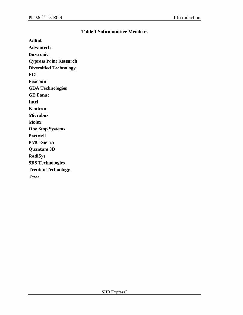
Table 1 Subcommittee Members
Adlink Advantech Bustronic Cypress Point Research Diversified Technology FCI Foxconn GDA Technologies GE Fanuc Intel Kontron Microbus Molex One Stop Systems Portwell PMC-Sierra Quantum 3D RadiSys SBS Technologies Trenton Technology Tyco

1 Introduction PICMG® 1.3 R0.9
SHB Express™ 5
1.4 Special Word Usage In this specification the following key words (in bold text) will be used:
may: indicates flexibility of choice with no implied preference. should: indicates flexibility of choice with a strongly preferred implementation. shall: indicates a mandatory requirement. Designers shall implement such
mandatory requirements to ensure interchangeability and to claim conformance with this specification.
1.5 Name And Logo Usage The PCI Industrial Computer Manufacturers Group’s policy regarding the use of the registered trademarks, PICMG ®, SHB Express™, and the PICMG ®, SHB Express™ logos is as follows:
• Any company may claim compatibility with PICMG ®, whether a member of the PICMG ® or not. Refer to PICMG Policies and Procedures Rev 1.1 Section 7.4.6 for claims of compliance language.
• Permission to use the PICMG ® and SHB Express™ logos is automatically granted to designated members only as stipulated on the most recent Membership Privileges document, during the period of time for which their membership dues are paid.
• A PICMG member’s distributors and sales representatives may use the PICMG ® and SHB Express™ logos in promoting a PICMG member’s products sold under the name of the member.
• The PICMG ® and SHB Express™ logos shall be printed in black or in color as illustrated on the Logo Page that is available from the PICMG ® at the address above. The center bar of the logos containing the phrase “PICMG ®” or “SHB Express™” is set horizontally and the aspect ratio of the logo shall be maintained, but the size may be varied. Nothing may be added to or deleted from the PICMG ® and SHB Express™ logos.
• Since the PICMG ® and SHB Express™ logos, and the PICMG ® and SHB Express™ names are registered trademarks of the PICMG ®, the following statement shall be included in all published literature and advertising material in which the logos appears:
PICMG ®, SHB Express™ and the PICMG ® and SHB Express™ logos are trademarks of the PCI Industrial Computer Manufacturers Group.
1.6 Signal Naming Conventions All signals are active high unless denoted by a trailing #. An active-high signal that is active (i.e., high), or an active-low signal that is active (i.e., low) is referred to herein as an asserted signal and the opposite signal state is referred to as deasserted. Differential signals are denoted by a trailing + or -.
PICMG® 1.3 R0.9 1 Introduction
SHB Express™
1.7 Intellectual Property The Intellectual Property guidelines outlined in the PICMG® Policies and Procedures for Specification Development would preclude the SHB Express™ (PICMG® 1.3) Specification from including any intellectual property not subject to a commitment by its owners to license under reasonable and non-discriminatory terms. The SHB Express™ Specification conforms to the Intellectual Property guidelines outlined in the PICMG Policies and Procedures for Specification Development, R1.1.
1 Introduction PICMG® 1.3 R0.9
SHB Express™ 7
1.8 Terminology It is expected that the reader has a basic understanding of the PCI Express specification.
All dimensions are specified in millimeters then inches in the following format: mm (inch). For example, 25.4mm (1”).
The following terms are used in specific ways throughout this document:
Backplane The board with the SHB slot and expansion slots.
Downstream 1. The relative position of an interconnect/system element (Port/component) that is farther from the Root Complex. The Ports on a Switch that are not the Upstream Port are Downstream Ports. All Ports on a Root Complex are Downstream Ports. The Downstream component on a Link is the component farther from the Root Complex. 2. A direction of information flow where the information is flowing away from the Root Complex.
Expansion board
A standard PCI, PCI-X, or PCIe board
SHB Express™ PICMG 1.3 System Host Board PCI Express specification.
Link A collection of one or more PCIe Lanes.
PCI In this specification, PCI is a generic designation that covers 32-bit (or 64bit on backplane only) PCI at 33/66MHz. A more specific designation is used when required.
PCIe In this specification, PCIe is a generic designation that covers x1, x4, x8, x16 PCI Express Base. A more specific designation is used when required
PCIe Lane One PCIe Lane contains two differential lines for Transmitter and two differential lines for Receiver.
PCI-X In this specification, PCI-X is a generic designation that covers 32-bit (or 64bit on backplane only) PCI-X at 33/66/100/133MHz. A more specific designation is used when required.
PCI(-X) In this specification, PCI(-X) is a generic designation that covers 32-bit (or 64bit on backplane only) PCI at 33/66MHz, as well as 32-bit PCI-X at 33/66/100/133MHz. A more specific designation is used when required.
Port 1. Logically, an interface between a component and a PCI Express Link. 2. Physically, a group of Transmitters and Receivers located on the same chip that define a Link.
Primary Bus 1. A PCI(-X) bus segment directly attached to the SHB through connector D

PICMG® 1.3 R0.9 1 Introduction
SHB Express™
2. A PCI(-X) bus segment directly attached to a PCIe-to-PCI(-X) bridge.
Root Complex Hierarchically the originator of the PCIe fabric.
SHB System Host Board. Refers to the removable CPU board that is the root complex of the system.
SHB slot The slot on an SHB Express™ backplane where you put the SHB. An SHB or electrically compliant board may populate this slot.
Upstream 1. The relative position of an interconnect/system element (Port/component) that is closer to the Root Complex. The Port on a Switch that is closest topologically to the Root Complex is the Upstream Port. The Port on an Endpoint or Bridge is an Upstream Port. The Upstream component on a Link is the component closer to the Root Complex. 2. A direction of information flow where the information is flowing towards the Root Complex.
xN A link with “N” physical lanes. “N” can be 1, 2, 4, 8, or 16 in this SHB Express™ specification (i.e. x1, x4, x8, or x16).

1 Introduction PICMG® 1.3 R0.9
SHB Express™ 9
This page intentionally left blank.
PICMG® 1.3 R0.9 2 Feature Set
SHB Express™
2 FEATURE SET
2.1 Form Factors The SHB Express™ SHB’s are defined in two form factors: full-size and half-size SHB’s (See Section 5). The full-size SHB length is identical to the ISA long board length and height. Half-size SHB form factor is based on the half-size PCIe and PCI board in length, while following the ISA board height.
2.2 System Composition An SHB Express™ system is composed of one SHB Express™ SHB and an SHB Express™ backplane. Expansion slots have 20.32mm (0.8”) board center-to-center spacing as defined in the PCI Express Card Electromechanical Specification.
The SHB should provide as many connections as possible with a minimum of one lane each of PCIe to the backplane. Physically the SHB slot may be located at any slot in the backplane. Electrically all SHB PCIe connections shall be the root complex AND/OR the most upstream port of the backplane. Mechanically, Connectors A, B, C, and, optionally, D should be present for a full-size SHB. Mechanically, Connectors A and B should be present for a half-size SHB.
A SHB Connector D should provide arbitration, clock distribution, and reset functions for all primary PCI(-X) expansion boards. A SHB is responsible for performing system initialization by managing each local board’s IDSEL signal on the PCI(-X) backplane. Physically the SHB slot may be located at any slot in the backplane. Electrically it shall be at the end of the primary PCI(-X) bus. Each Connector may have up to the following: Connector A: (One link of x16 PCIe) OR (two links of x8 PCIe) OR (one link of x8 PCIe
AND two links of x4 PCIe) OR (four links of x4 PCIe) Connector B: (One link of x4 PCIe) OR (four links of x1 PCIe). Connector C: Additional power and I/O. Connector D: One 32-bit PCI(-X) bus.
The SHB may connect IPMB, PCI wake up, ATX support, Ethernet, USB, and SATA to the backplane.
2.3 Connectors For reference purposes, the connectors are lettered from A through D starting at the I/O bracket end of the board. Table 2 shows the physical connectors specified for the SHB. Mechanically all SHB connectors are defined in the PCI Express Card Electromechanical Specification.

2 Feature Set PICMG® 1.3 R0.9
SHB Express™ 11
Table 2 SHB Connectors
Connector Type Pin Count
A x16 164 B x8 98 C x16 164 D x8 98
On the full-size SHB and backplane there should be two (2) x16 PCI Express connectors (A and C) and two (2) x8 PCI Express connectors (B and D). On the half-size SHB and backplane there shall be one x16 PCI Express Connector (A) and one x8 PCI Express Connector (B).
See Section 4.1 for a detailed pinout of all four connectors.
2.4 Optional ATX or BTX Power Supply Support A SHB may implement ATX or BTX power supply support. Also, an SHB Express™ backplane may implement ATX or BTX support and the system power supply may be ATX or BTX. All ATX/non-ATX/BTX/non-BTX combinations are valid and covered to avoid interoperability problems while keeping this feature fully operational.
PICMG® 1.3 R0.9 2 Feature Set
SHB Express™
This page intentionally left blank.
3 Electrical Requirements PICMG® 1.3 R0.9
SHB Express™ 13
3 ELECTRICAL REQUIREMENTS
3.1 PCIe Compliance Connectors A and B of the SHB and backplane that utilizes PCIe shall adhere to the PCI Express Base Specification.
An SHB Express™ SHB and backplane, if utilizing the PCI connection shall adhere to the PCI Local Bus Specification and to the PCI-to-PCI Bridge Architecture Specification. Depending on their capabilities, they might have to adhere to the PCI-X Addendum to the PCI Local Bus Specification and the PCI Bus Power Management Interface Specification. This chapter documents additional requirements and/or restrictions as needed.
3.2 Signals Overview
Table 3 SHB Slot Signal Groups
Type Signals Description Connector Source GND, +5V, +3.3V, +12V Power backplane
+3.3Vaux Optional standby supply A backplane
PWRGD, PSON#, PWRBT#, +5Vaux Optional ATX support A and B backplane
TRST#, TCK, TMS, TDI, TDO Optional JTAG support A SHB
SMCLK, SMDAT Optional SMBus support A SHB
VIO Match keying for PCI bus D backplane
IPMB_CL, IPMB_DA Optional IPMB support C SHB
CFG[0:3] PCIe configuration straps A backplane
GA[0:5] Reserved for optional geographic addressing for IPMB
C SHB
SHB_RST# Optional reset line A SHB RSVD Reserved A and B RSVD-G Reserved ground A backplane
Global
WAKE# Signal for link reactivation A backplane

PICMG® 1.3 R0.9 3 Electrical Requirements
SHB Express™
a_PETp[0:15], a_PETn[0:15], a_PERp[0:15], a_PERn[0:15]
Point-to-point from SHB slot through the x16 PCIe Connector (A) to the target device(s)
A and B SHB
b_PETp[0:7], b_PETn[0:7], b_PERp[0:7], b_PERn[0:7]
Point-to-point from SHB slot through the x8 PCIe Connector (B) to the target device(s)
A SHB PCIe
REFCLK[0:7]+, REFCLK[0:7]-
Clock synchronization of PCIe expansion slots A SHB
AD[0:31], FRAME#, IRDY#, TRDY#, STOP#, LOCK#, DEVSEL#, PERR#, SERR#, C/BE[0:3], SDONE, SBO#
Bussed on SHB slot and expansion slots
D SHB
REQ[0:3], GNT[0:3], CLKA, CLKB, CLKC, CLKD
Point-to-point from SHB slot to each expansion slot
D SHB
INTA#, INTB#, INTC#, INTD#
Bussed (rotating) on SHB slot and expansion slots
D backplane
M66EN, PCIXCAP Bussed on SHB slot and expansion slots D SHB
PCI(-X)
PME#
Optional PCI wake-up event bussed on SHB and backplane expansion slots
A SHB
USB[0:3]P, USB[0:3]N, USBOC[0:3]#
Optional point-to-point from SHB Connector C to a destination USB device
C SHB
SATAHT[0:1]P, SATAHT[0:1]N, SATAHR[0:1]P, SATAHR[0:1]N
Optional point-to-point from SHB Connector C to a destination SATA device
C SHB Miscellaneous I/O
a_MDI[0:3]p, a_MDI[0:3]n, b_MDI[0:3]p, b_MDI[0:3]n
Optional point-to-point from SHB Connector C to a destination Ethernet device
C SHB

3 Electrical Requirements PICMG® 1.3 R0.9
SHB Express™ 15
3.3 SHB Design Rules
3.3.1 PCIe Signals
Table 4 below shows the possible link configurations. Note that B0 can also be four x1 ports.
Table 4 PCIe Link Configurations
A0
(x16)
A2 (x8)
A0 (x8)
B0 (x4)
Con
figur
atio
n
A3 (x4)
A2 (x4)
A1 (x4)
A0 (x4)
Ref Clks for all ports (up to 8 clks)
B3
(x1)B2
(x1)B1
(x1)B0(x1)
c1 x16 (Ref Clks) x4 c2 second x8 first x8 (Ref Clks) x4 c3 third x4 second x4 x8 (Ref Clks) first x4 c4 fifth x4 fourth x4 third x4 second x4 (Ref Clks) first x4
A backplane should plumb the PCIe in the following order to maximize interoperability: c5 8th 7th 6th 5th 4th 3rd 2nd 1st All SHB Express™ SHB’s should provide at least x1 PCIe to all possible links. Below are examples of possible PCIe applications through both Connector A and B. Note that PEXx refers to the PCIe links where “X” is either “T”ransmit or “R”eceive, and “x” is either “p”ositive or “n”egative differential pairs. The ports for the A[3:0] links shall be configured in one of the following ways:
Up to (1) x16 PCIe OR Up to (2) x8 PCIe OR Up to (2) x4 PCIe AND (1) x8 PCIe OR Up to (4) x4 PCIe
a_PEXx[0:15] (A0)
a_PEXx[8:15] (A2)
a_PEXx[0:7] (A0)
a_PEXx [12:15]
(A3)
a_PEXx [8:11] (A2)
a_PEXx [0:7] (A0)
a_PEXx [12:15]
(A3)
a_PEXx [8:11] (A2)
a_PEXx [4:7] (A1)
a_PEXx [0:3] (A0)
PICMG® 1.3 R0.9 3 Electrical Requirements
SHB Express™
The ports for the B[3:0] links shall be configured in one of the following ways:
Up to (1) x4 PCIe
OR Up to (4) x1 PCIe
Figure 1 Possible Link Configurations
The PCIe signals (PETp[0:15], PETn[0:15], PERp[0:15], PERn[0:15], REFCLK+ and REFCLK-) that are not used shall be pulled up with a 8.2k Ohm resistor to 3.3V. All PCIe links should support x1 PCIe as a minimum. Optionally, the x16 link may support x1, x4, x8, and x16. The x8 PCIe link may support x1, x4, and x8. The x4 PCIe link may support x1 and x4. The x1 PCIe link may support x1 only.
3.3.2 PCIe Differential Clocks to Link Association
If the SHB supplies a specific link to the backplane, then the SHB shall supply the associated differential clock. If a link can be broken down into multiple links, the SHB shall provide every clock that might be used on the backplane. For example, if the SHB provides A0 as a single x8, and that link could work as two x4 links, then the SHB shall provide REFCLK4 and REFCLK5.
Table 5 Differential Clock to PCIe Link Association Differential
Clock PCIe link
REFCLK0 B0 REFCLK1 B1 REFCLK2 B2 REFCLK3 B3 REFCLK4 A0 REFCLK5 A1 REFCLK6 A2 REFCLK7 A3
3.3.3 PCIe Insertion Loss
The maximum loss values in dB (decibels) are specified for the SHB and the PCIe
(Ref Clocks)
b_PEXx[0:3] (B0)
(Ref Clocks) b_
PEX
x3
(B3)
b_
PEX
x2
(B2)
b_
PEX
x1
(B1)
b_
PEX
x0
(B0)
3 Electrical Requirements PICMG® 1.3 R0.9
SHB Express™ 17
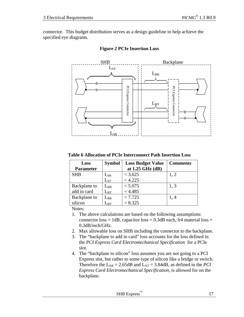
connector. This budget distribution serves as a design guideline to help achieve the specified eye diagrams.
Figure 2 PCIe Insertion Loss
SHB Backplane
LST LBR
LBT
LSR
Table 6 Allocation of PCIe Interconnect Path Insertion Loss
Loss Parameter
Symbol Loss Budget Value at 1.25 GHz (dB)
Comments
SHB LSR LST
< 3.625 < 4.225
1, 2
Backplane to add in card
LBR LBT
< 5.075 < 4.485
1, 3
Backplane to silicon
LBR LBT
< 7.725 < 8.325
1, 4
Notes: 1. The above calculations are based on the following assumptions:
connector loss = 1dB, capacitor loss = 0.3dB each, fr4 material loss = 0.3dB/inch/GHz.
2. Max allowable loss on SHB including the connector to the backplane. 3. The “backplane to add in card” loss accounts for the loss defined in
the PCI Express Card Electromechanical Specification for a PCIe slot.
4. The “backplane to silicon” loss assumes you are not going to a PCI Express slot, but rather to some type of silicon like a bridge or switch. Therefore the LAR = 2.65dB and LAT = 3.84dB, as defined in the PCI Express Card Electromechanical Specification, is allowed for on the backplane.
PCI Express C
onnector
PCI Express C
onnector

PICMG® 1.3 R0.9 3 Electrical Requirements
SHB Express™
3.3.4 USB Insertion Loss
The maximum loss values in dB (decibels) are specified for the SHB and backplane. This budget distribution serves as a design guideline to help achieve the specified eye diagrams.
Figure 3 USB Insertion Loss
SHB Backplane
LS LB
Table 7 Allocation of USB Interconnect Path Insertion Loss
Loss Parameter
Symbol Loss Budget Value at 250 MHz (dB)
Comments
SHB LS < 0.45 1, 2 Backplane to USB connector
LB < 0.9 1, 3, 4
Notes: 1. The above calculations are based on the following assumption: fr4
material loss = 0.3dB/inch/GHz. 2. Max allowable loss on SHB including the connector to the backplane. 3. The “Backplane to USB connector” loss accounts for the loss defined
in the Universal Serial Bus Revision 2.0 specification. 4. Appropriate overcurrent protection shall be provided for each USB
connection available on the backplane.
PCI Express
Connector
USB
C
onnector
Overcurrent
Protection

3 Electrical Requirements PICMG® 1.3 R0.9
SHB Express™ 19
3.3.5 SATA Insertion Loss
The maximum loss values in dB (decibels) are specified for the SHB and backplane. This budget distribution serves as a design guideline to help achieve the specified eye diagrams.
Figure 4 SATA Insertion Loss
SHB Backplane
LS LR LB
LS LR LB
Table 8 Allocation of SATA Interconnect Path Insertion Loss
Loss Parameter Symbol Loss Budget Value at 1.5 GHz SATAI
or 3.0 GHz SATAII (dB)
Comments
SHB LS < 1.4 1, 2 PCIe connector to Repeater
LR < 0.4 1, 3, 4
Repeater to SATA connector
LB < 1.8 1, 4
Notes: 1. The above calculations are based on the following assumptions:
connector loss = 1dB, fr4 material loss = 0.3dB/inch/GHz. 2. Max allowable loss on SHB including the connector to the backplane. 3. Appropriate repeaters should be provided for each SATA connection
available on the SHB. 4. Max allowable SATA loss total is 1.8 dB.
SATA
Connector
Repeater
PCI Express C
onnector

PICMG® 1.3 R0.9 3 Electrical Requirements
SHB Express™
3.3.6 10/100/1000 Ethernet Insertion Loss
The maximum loss values in dB (decibels) are specified for the SHB and backplane. This budget distribution serves as a design guideline to help achieve the specified eye diagrams.
Figure 5 Ethernet Insertion Loss
SHB Backplane
LS LB
LS LB
Table 9 Allocation of Ethernet Interconnect Path Insertion Loss
Loss Parameter
Symbol Loss Budget Value at 500 MHz (dB)
Comments
SHB LS < 0.9 1, 2, 3 Backplane to Ethernet connector
LB < 0.9 1, 4
Notes: 5. The above calculations are based on the following assumption: fr4
material loss = 0.3dB/inch/GHz. 6. Max allowable loss on SHB including the connector to the backplane. 7. Appropriate magnetics shall be provided for each ethernet connection
available on the SHB. 8. The “Backplane to USB connector” loss accounts for the loss defined
in the IEEE Std 802.3 – 2002 chapter 40.7.
3.3.7 Optional JTAG/Boundary Scan Signals
A SHB with no JTAG capability shall connect TDI to TDO and leave TRST#, TMS and TCK unconnected.
PCI Express C
onnector
Ethernet Connector
Magnetics
3 Electrical Requirements PICMG® 1.3 R0.9
SHB Express™ 21
3.3.8 Optional IPMB Signals
A SHB that does not support IPMB shall leave IPMB_CL and IPMB_DA unconnected.
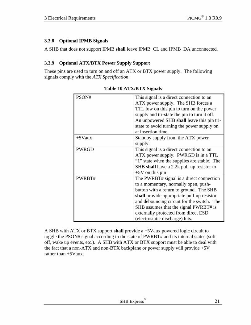
3.3.9 Optional ATX/BTX Power Supply Support
These pins are used to turn on and off an ATX or BTX power supply. The following signals comply with the ATX Specification.
Table 10 ATX/BTX Signals
PSON# This signal is a direct connection to an ATX power supply. The SHB forces a TTL low on this pin to turn on the power supply and tri-state the pin to turn it off. An unpowered SHB shall leave this pin tri-state to avoid turning the power supply on at insertion time.
+5Vaux Standby supply from the ATX power supply.
PWRGD This signal is a direct connection to an ATX power supply. PWRGD is in a TTL “1” state when the supplies are stable. The SHB shall have a 2.2k pull-up resistor to +5V on this pin
PWRBT# The PWRBT# signal is a direct connection to a momentary, normally open, push-button with a return to ground. The SHB shall provide appropriate pull-up resistor and debouncing circuit for the switch. The SHB assumes that the signal PWRBT# is externally protected from direct ESD (electrostatic discharge) hits.
A SHB with ATX or BTX support shall provide a +5Vaux powered logic circuit to toggle the PSON# signal according to the state of PWRBT# and its internal states (soft off, wake up events, etc.). A SHB with ATX or BTX support must be able to deal with the fact that a non-ATX and non-BTX backplane or power supply will provide +5V rather than +5Vaux.
PICMG® 1.3 R0.9 3 Electrical Requirements
SHB Express™
3.3.10 +3.3Vaux Supply
Voltage shall be supplied to the +3.3Vaux pins on the SHB slot.
3.3.11 Optional USB and SATA Signals
If an SHB supports USB it shall terminate USB[0:3]P and USB[0:3]N as described in the Universal Serial Bus Specification.
A SHB with no support for USB and/or SATA shall leave these pins unconnected.
3.3.12 Optional SMBus Signals
The SHB shall have 8.2k Ohm resistor pull-ups on SMCLK and SMDAT. The pull-ups shall be connected to 3.3Vaux unless 3.3Vaux is not supported, in which case the pull-ups shall be connected directly to 3.3V.
3.3.13 Optional IPMB Signals
The SHB shall pull-up IPMB_CL and IPMB_DA with 8.2k Ohm resistors to 3.3Vaux unless 3.3Vaux is not supported, in which case the pull-ups shall be connected directly to 3.3V.
3.3.14 Optional WAKE# Signal
The SHB shall pull-up WAKE# with an 8.2k Ohm resistor to 3.3V. The pull-up shall be connected to 3.3Vaux unless 3.3Vaux is not supported, in which case the pull-up shall be connected directly to 3.3V.
3.3.15 SHB_RST# Signal
The SHB shall pull-up SHB_RST# with an 8.2k Ohm resistor to 3.3V. The SHB_RST# signal is a direct connection to a momentary, normally open, push-button with a return to ground.
3.3.16 PCI REQ#/GNT# Signal Additions
A SHB should provide all four REQ#/GNT# pairs. If some REQ#/GNT# pairs are not available, the SHB shall provide the available REQ#/GNT# pairs starting from REQ0#/GNT0# through REQ3#/GNT3#. Any unused GNT# signals on a SHB shall have a strong pull-up resistor to +5V to avoid floating the GNT# signal of an expansion board.
For example, a +5V SHB Express™ SHB providing 3 pairs of REQ#/GNT# will leave REQ3# unconnected and GNT3# pulled to +5V.
3 Electrical Requirements PICMG® 1.3 R0.9
SHB Express™ 23
3.3.17 PCI M66EN Signal
A SHB that does not support 66MHz PCI signaling on a bus shall ground the corresponding M66EN pin.
3.3.18 PCI-X PCIXCAP Signal
A SHB with no PCI-X capability on a bus shall ground the corresponding PCIXCAP pin.
3.3.19 Non-PCI Bus Implementation
A full size SHB (with Connector D present) that does not support the PCI bus shall leave all PCI signals unconnected except for PCI_RST#, which shall be pulled to GND via a 100 Ohms resistor on the SHB.
PICMG® 1.3 R0.9 3 Electrical Requirements
SHB Express™
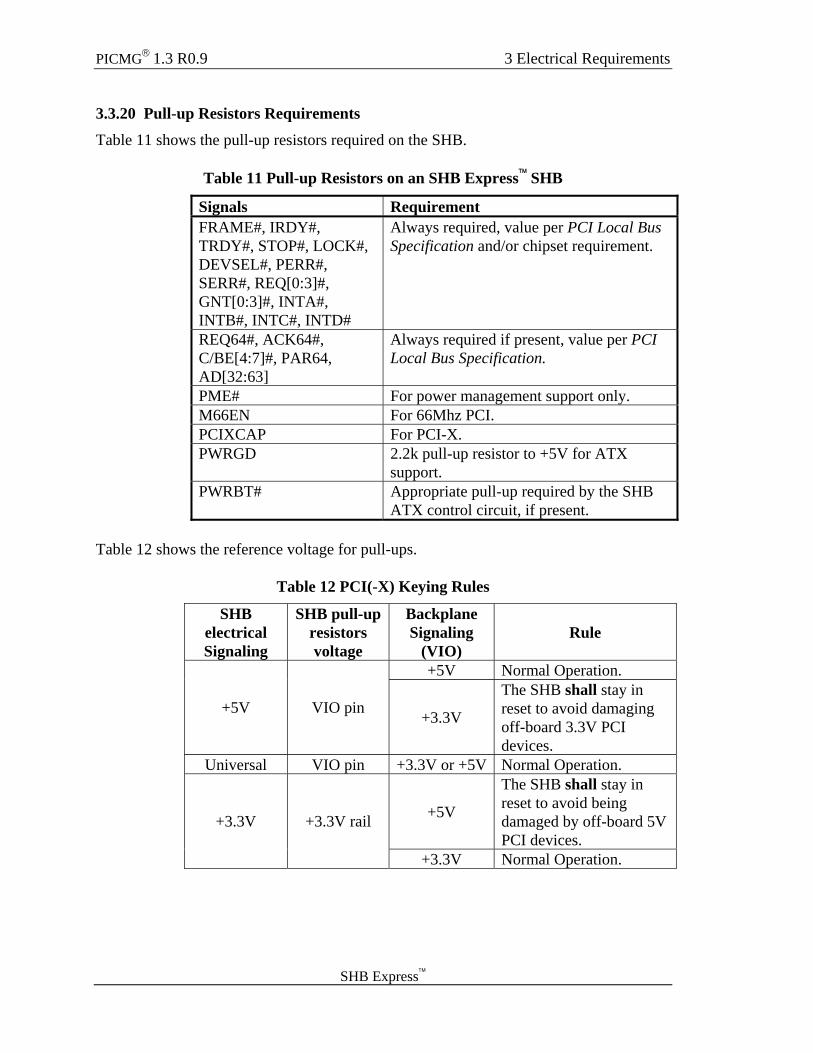
3.3.20 Pull-up Resistors Requirements
Table 11 shows the pull-up resistors required on the SHB.
Table 11 Pull-up Resistors on an SHB Express™ SHB
Signals Requirement FRAME#, IRDY#, TRDY#, STOP#, LOCK#, DEVSEL#, PERR#, SERR#, REQ[0:3]#, GNT[0:3]#, INTA#, INTB#, INTC#, INTD#
Always required, value per PCI Local Bus Specification and/or chipset requirement.
REQ64#, ACK64#, C/BE[4:7]#, PAR64, AD[32:63]
Always required if present, value per PCI Local Bus Specification.
PME# For power management support only. M66EN For 66Mhz PCI. PCIXCAP For PCI-X. PWRGD 2.2k pull-up resistor to +5V for ATX
support. PWRBT# Appropriate pull-up required by the SHB
ATX control circuit, if present. Table 12 shows the reference voltage for pull-ups.
Table 12 PCI(-X) Keying Rules
SHB electrical Signaling
SHB pull-up resistors voltage
Backplane Signaling
(VIO) Rule
+5V Normal Operation.
+5V VIO pin +3.3V
The SHB shall stay in reset to avoid damaging off-board 3.3V PCI devices.
Universal VIO pin +3.3V or +5V Normal Operation.
+5V
The SHB shall stay in reset to avoid being damaged by off-board 5V PCI devices.
+3.3V +3.3V rail
+3.3V Normal Operation.
3 Electrical Requirements PICMG® 1.3 R0.9
SHB Express™ 25
3.3.21 SHB Express™ SHB PCI(-X) Clock Feedback (CLKFO/CLKFI)
A SHB may use the clock feedback from the backplane to minimize clock skew. If it does, it shall output a PCI clock on the CLKFO pin and read it back on the CLKFI pin.
If the clock feedback is not used, CLKFO and CLKFI shall be grounded.
3.3.22 Reserved Pins
A SHB shall leave unconnected all reserved pins marked as RSVD.
3.3.23 Reserved-Ground Pins
A SHB shall leave unconnected all reserved pins marked as RSVD-G.
3.4 Backplane Design Rules
3.4.1 PCB Characteristics
If an SHB Express™ backplane is PCIe ready, it shall comply with the PCIe requirements for the printed circuit board as described in the PCI Express Base Specification. The SHB Express™ backplane shall have a characteristic impedance of 100 Ohms +/- 10% differential impedance, and conform to the PCIe rules for trace spacing for all PCIe signals.
If an SHB Express™ backplane is PCI(-X) ready, it shall comply with PCI(-X) requirements for the printed circuit board as described in the PCI Local Bus Specification and PCI-X Addendum to the PCI Local Bus Specification. The SHB Express™ backplane shall have a characteristic impedance of 57 Ohms +/- 10% and conform to the PCI(-X) rules for trace spacing for all PCI(-X) signals.
3.4.2 PCI IDSEL Assignment for Primary PCI Busses
The backplane shall make the IDSEL connection at each expansion slot or device through a resistor as defined in the PCI Local Bus Specification. This resistor shall be placed to minimize the stub on the ADxx line. The SHB shall use AD[28:31] point-to-point to each expansion slot on the primary bus.
A backplane should implement slot IDSEL on the primary bus starting with AD31 and going sequentially down in a secondary ADxx number.
3.4.3 PCI Interrupt Binding
The interrupt binding on the primary bus is identical to the PICMG 1.0 and 1.2 specification. The secondary binding complies with the PCI-to-PCI Bridge Architecture Specification. The primary bus is defined as either:
PICMG® 1.3 R0.9 3 Electrical Requirements
SHB Express™
1. A PCI(-X) bus segment directly attached to the SHB through connector D 2. A PCI(-X) bus segment directly attached to a PCIe-to-PCI(-X) bridge.
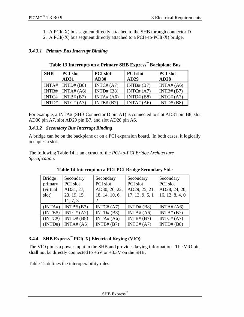
3.4.3.1 Primary Bus Interrupt Binding
Table 13 Interrupts on a Primary SHB Express™ Backplane Bus
SHB PCI slot AD31
PCI slot AD30
PCI slot AD29
PCI slot AD28
INTA# INTD# (B8) INTC# (A7) INTB# (B7) INTA# (A6) INTB# INTA# (A6) INTD# (B8) INTC# (A7) INTB# (B7) INTC# INTB# (B7) INTA# (A6) INTD# (B8) INTC# (A7) INTD# INTC# (A7) INTB# (B7) INTA# (A6) INTD# (B8)
For example, a INTA# (SHB Connector D pin A1) is connected to slot AD31 pin B8, slot AD30 pin A7, slot AD29 pin B7, and slot AD28 pin A6.
3.4.3.2 Secondary Bus Interrupt Binding
A bridge can be on the backplane or on a PCI expansion board. In both cases, it logically occupies a slot.
The following Table 14 is an extract of the PCI-to-PCI Bridge Architecture Specification.
Table 14 Interrupt on a PCI-PCI Bridge Secondary Side
Bridge primary (virtual slot)
Secondary PCI slot AD31, 27, 23, 19, 15, 11, 7, 3
Secondary PCI slot AD30, 26, 22, 18, 14, 10, 6, 2
Secondary PCI slot AD29, 25, 21, 17, 13, 9, 5, 1
Secondary PCI slot AD28, 24, 20, 16, 12, 8, 4, 0
(INTA#) INTB# (B7) INTC# (A7) INTD# (B8) INTA# (A6) (INTB#) INTC# (A7) INTD# (B8) INTA# (A6) INTB# (B7) (INTC#) INTD# (B8) INTA# (A6) INTB# (B7) INTC# (A7) (INTD#) INTA# (A6) INTB# (B7) INTC# (A7) INTD# (B8)
3.4.4 SHB Express™ PCI(-X) Electrical Keying (VIO)
The VIO pin is a power input to the SHB and provides keying information. The VIO pin shall not be directly connected to +5V or +3.3V on the SHB.
Table 12 defines the interoperability rules.

3 Electrical Requirements PICMG® 1.3 R0.9
SHB Express™ 27
3.4.5 64-bit PCI(-X)
REQ64#, ACK64#, PAR64, AD[32:63], and C/BE[4:7] signals shall be pulled-up or pulled-down per the PCI Local Bus Specification.
3.4.6 PCI(-X) M66EN and PCIXCAP Signals
The M66EN and PCIXCAP signals shall be bussed on all connectors on a given bus. Each expansion slot shall implement a 0.01uF capacitor within 0.25” of the physical slots as per PCI-X Addendum to the PCI Local Bus Specification on the M66EN and PCIXCAP signals.
If an SHB Express™ backplane has speed limitations because of its bus topology, length, or number of slots, it should restrict bus speed by placing appropriate pull-down resistor or ground connections on M66EN and PCIXCAP signals according to the PCI-X Addendum to the PCI Local Bus Specification.
3.4.7 Optional JTAG/Boundary Scan Signals
An SHB Express™ backplane with JTAG capability may provide access to the JTAG portion of the SHB slot.
3.4.8 Optional IPMB Signals
An SHB Express™ backplane with IPMB capability may provide access to the SHB slot IPMB signals IPMB_CL and IPMB_DA. If IPMB is not supported on the backplane then these pins should be left unconnected.
3.4.9 Pull-up Resistors Requirements
Table 15 shows the pull-up resistors required on the backplane.
Table 15 Pull-up Resistors on an SHB Express™ Backplane
Signals Requirement AD[32:63], C/BE[4:7]#, PAR64
If present, always required, value per PCI Local Bus Specification.
PCIXCAP If present, always required, value per PCI-X Addendum to the PCI Local Bus Specification if running in PCI-X mode.
3.4.10 SHB Express™ Backplane PCI(-X) Slot Clock Feedback
An SHB Express™ Backplane may use the clock feedback from the SHB to minimize clock skew. If it does, it shall use CLKF0 and CLKF1 in making the feedback clock longer than the 1” allowed for on the SHB.
PICMG® 1.3 R0.9 3 Electrical Requirements
SHB Express™
If the clock feedback is not used, CLKF0 and CLKF1 shall be either grounded or floating.
3.4.11 ATX/BTX Power Supply Support
All backplanes with ATX, BTX or equivalent capability shall route PSON#, +5Vaux and PWROK from the ATX or BTX connector to the SHB slot. All backplanes shall have a 2 pin header with 2.54mm (0.1”) spacing used to turn on the power supply. This header will provide a means to connect a momentary push-button (local or remote). Pin 1 shall be PWRBT# and pin 2 shall be ground. The backplane should have some form of jumper or strapping option on PSON# to be able to turn on or off an ATX, BTX, or equivalent power supply when the SHB has no power supply control capability.
If the backplane (or the power supply) has no ATX or BTX connector, it shall leave the SHB slot pins PWRBT#, PSON#, and PWRGD floating. It shall also route +5V to the +5Vaux pins on the SHB slot.
3.4.12 +3.3Vaux Supply
If a +3.3Vaux standby voltage is available it shall be routed to the SHB slot. If the +3.3Vaux standby voltage is not available then standard 3.3V shall be provided to the +3.3Vaux pins on the SHB slot. +3.3Vaux standby voltage may be provided to the backplane peripheral slots.
3.4.13 SHB_RST# Signal
All backplanes shall have a 2 pin header with 2.54mm (0.1”) spacing used to reset the power supply. Pin 1 shall be SHB_RST# and pin 2 shall be ground.
3.4.14 Power Distribution
As per PCI Express Base Specification, an SHB Express™ backplane shall provide +5V, +3.3V, and +12V with +/-5% tolerance.
The backplane PCB should provide separate power planes for +3.3V, +5V, +12V and ground.
3.4.15 SHB Express™ SMCLK and SMDAT
If the backplane is capable of supporting SMBus (SMCLK and SMDAT signals), the signals shall be bussed between the SHB slot and the corresponding pins on expansion
3 Electrical Requirements PICMG® 1.3 R0.9
SHB Express™ 29
slots (see System Management Bus (SMBus) Specification, and Intelligent Platform Management Interface Specification.).
A backplane that is not capable of supporting SMBus (i.e. a backplane with no PCIe slots) shall leave these pins unconnected.
3.4.16 Optional USB, SATA, and Ethernet Signals
A backplane with no support for USB, SATA and/or Ethernet shall leave these pins unconnected.
3.4.17 WAKE# Signal
A backplane shall route WAKE# to all PCIe devices and SHB slot.
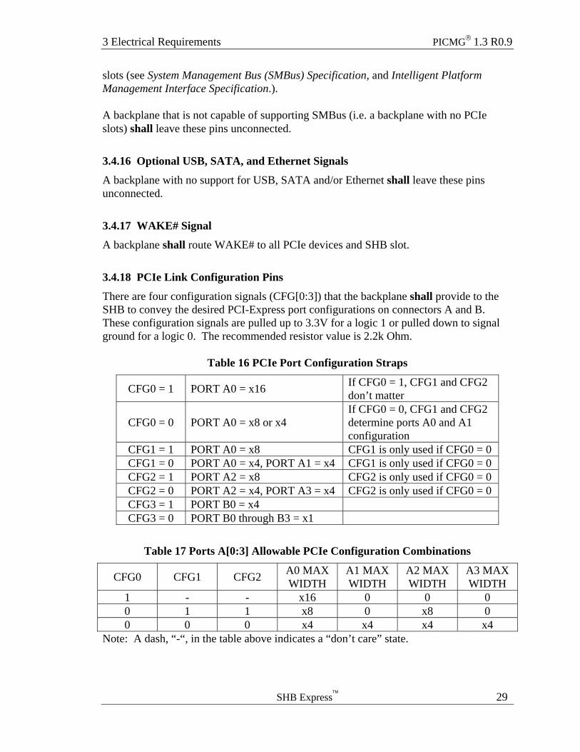
3.4.18 PCIe Link Configuration Pins
There are four configuration signals (CFG[0:3]) that the backplane shall provide to the SHB to convey the desired PCI-Express port configurations on connectors A and B. These configuration signals are pulled up to 3.3V for a logic 1 or pulled down to signal ground for a logic 0. The recommended resistor value is 2.2k Ohm.
Table 16 PCIe Port Configuration Straps
CFG0 = 1 PORT A0 = x16 If CFG0 = 1, CFG1 and CFG2 don’t matter
CFG0 = 0 PORT A0 = x8 or x4 If CFG0 = 0, CFG1 and CFG2 determine ports A0 and A1 configuration
CFG1 = 1 PORT A0 = x8 CFG1 is only used if CFG0 = 0 CFG1 = 0 PORT A0 = x4, PORT A1 = x4 CFG1 is only used if CFG0 = 0 CFG2 = 1 PORT A2 = x8 CFG2 is only used if CFG0 = 0 CFG2 = 0 PORT A2 = x4, PORT A3 = x4 CFG2 is only used if CFG0 = 0 CFG3 = 1 PORT B0 = x4 CFG3 = 0 PORT B0 through B3 = x1
Table 17 Ports A[0:3] Allowable PCIe Configuration Combinations
CFG0 CFG1 CFG2 A0 MAX WIDTH
A1 MAX WIDTH
A2 MAX WIDTH
A3 MAX WIDTH
1 - - x16 0 0 0 0 1 1 x8 0 x8 0 0 0 0 x4 x4 x4 x4
Note: A dash, “-“, in the table above indicates a “don’t care” state.
PICMG® 1.3 R0.9 3 Electrical Requirements
SHB Express™
3.4.19 Reserved Pins
An SHB Express™ backplane shall leave unconnected all reserved pins marked as RSVD.
3.4.20 Reserved-Ground Pins
An SHB Express™ backplane shall pull-down with an 8.2k Ohm resistor all reserved pins marked as RSVD-G.
3.4.21 PCI_RST# Signal
A backplane with PCI(-X) support shall pull down PCI_RST# with a 8.2k Ohm resistor for the case where Connector D is not supplied from the SHB.
3 Electrical Requirements PICMG® 1.3 R0.9
SHB Express™ 31
This page intentionally left blank.
PICMG® 1.3 R0.9 4 PCI Express and PCI(-X) Interfaces
SHB Express™
4 PCI EXPRESS AND PCI(-X) INTERFACES
4.1 Connector Pinout Table 18 SHB Express™ Connector Pinout
x16 PCIe Connector A x8 PCIe Connector B x16 PCIe Connector C x8 PCIe Connector D
Side B Side A Side B Side A Side B Side A Side B Side A 1 SMCLK SMDAT 1 +5Vaux +5Vaux 1 USB0P GND 1 INTB# INTA# 2 GND GND 2 GND RSVD 2 USB0N GND 2 INTD# INTC# 3 TDI TCK 3 a_PETp8 GND 3 GND USB1P 3 GND VIO 4 TDO TMS 4 a_PETn8 GND 4 GND USB1N 4 REQ3# GNT3# 5 TRST# WAKE# 5 GND a_PERp8 5 USB2P GND 5 REQ2# GNT2# 6 PWRBT# PME# 6 GND a_PERn8 6 USB2N GND 6 PCI_RST# GNT1# 7 PWRGD PSON# 7 a_PETp9 GND 7 GND USB3P 7 REQ1# GNT0# 8 SHB_RST# PERST# 8 a_PETn9 GND 8 GND USB3N 8 REQ0# SERR# 9 CFG0 CFG1 9 GND a_PERp9 9 USBOC0# GND 9 SDONE +3.3V
10 CFG2 CFG3 10 GND a_PERn9 10 GND USBOC1# 10 GND CLKFI 11 RSVD GND 11 RSVD GND 11 USBOC2# GND 11 CLKFO GND Mechanical Key Mechanical Key Mechanical Key Mechanical Key
12 GND RSVD 12 GND RSVD 12 GND USBOC3# 12 CLKC CLKD 13 b_PETp0 GND 13 a_PETp10 GND 13 SATAHT0P GND 13 GND +3.3V 14 b_PETn0 GND 14 a_PETn10 GND 14 SATAHT0N GND 14 CLKA CLKB 15 GND b_PERp0 15 GND a_PERp10 15 GND SATAHR0P 15 +3.3V GND 16 GND b_PERn0 16 GND a_PERn10 16 GND SATAHR0N 16 AD31 PME# 17 b_PETp1 GND 17 a_PETp11 GND 17 SATAHT1P GND 17 AD29 +3.3V 18 b_PETn1 GND 18 a_PETn11 GND 18 SATAHT1N GND 18 M66EN AD30 19 GND b_PERp1 19 GND a_PERp11 19 GND SATAHR1P 19 AD27 AD28 20 GND b_PERn1 20 GND a_PERn11 20 GND SATAHR1N 20 AD25 GND 21 b_PETp2 GND 21 a_PETp12 GND 21 a_MDI0p GND 21 GND AD26 22 b_PETn2 GND 22 a_PETn12 GND 22 a_MDI0n GND 22 C/BE3# AD24 23 GND b_PERp2 23 GND a_PERp12 23 GND a_MDI1p 23 AD23 +3.3V 24 GND b_PERn2 24 GND a_PERn12 24 GND a_MDI1n 24 GND AD22 25 b_PETp3 GND 25 a_PETp13 GND 25 a_MDI2p GND 25 AD21 AD20 26 b_PETn3 GND 26 a_PETn13 GND 26 a_MDI2n GND 26 AD19 PCIXCAP 27 GND b_PERp3 27 GND a_PERp13 27 GND a_MDI3p 27 +5V AD18 28 GND b_PERn3 28 GND a_PERn13 28 GND a_MDI3n 28 AD17 AD16 29 REFCLK0+ GND 29 a_PETp14 GND 29 IPMB_CL GND 29 C/BE2# GND 30 REFCLK0- GND 30 a_PETn14 GND 30 IPMB_DA GND 30 GND FRAME# 31 GND REFCLK1+ 31 GND a_PERp14 31 GA0 GA1 31 IRDY# TRDY# 32 RSVD-G REFCLK1- 32 GND a_PERn14 32 GA2 GA4 32 DEVSEL# +5V 33 REFCLK2+ GND 33 a_PETp15 GND 33 GA3 GA5 33 LOCK# STOP# 34 REFCLK2- GND 34 a_PETn15 GND 34 b_MDI0p GND 34 PERR# GND 35 GND REFCLK3+ 35 GND a_PERp15 35 b_MDI0n GND 35 GND C/BE1# 36 RSVD-G REFCLK3- 36 GND a_PERn15 36 GND b_MDI1p 36 PAR AD14 37 REFCLK4+ GND 37 RSVD GND 37 GND b_MDI1n 37 SB0# GND 38 REFCLK4- GND 38 RSVD RSVD 38 b_MDI2p GND 38 GND AD12 39 GND REFCLK5+ 39 GND GND 39 b_MDI2n GND 39 AD15 AD10 40 RSVD-G REFCLK5- 40 GND GND 40 GND b_MDI3p 40 AD13 GND 41 REFCLK6+ GND 41 GND GND 41 GND b_MDI3n 41 GND AD09 42 REFCLK6- GND 42 GND GND 42 +3.3V +3.3V 42 AD11 C/BE0# 43 GND REFCLK7+ 43 GND GND 43 +3.3V +3.3V 43 AD08 GND

4 PCI Express and PCI(-X) Interfaces PICMG® 1.3 R0.9
SHB Express™ 33
x16 PCIe Connector A x8 PCIe Connector B x16 PCIe Connector C x8 PCIe Connector D Side B Side A Side B Side A Side B Side A Side B Side A 44 GND REFCLK7- 44 +12V +12V 44 +3.3V +3.3V 44 GND AD06 45 a_PETp0 GND 45 +12V +12V 45 +3.3V +3.3V 45 AD07 AD05 46 a_PETn0 GND 46 +12V +12V 46 +3.3V +3.3V 46 AD04 GND 47 GND a_PERp0 47 +12V +12V 47 +3.3V +3.3V 47 GND AD02 48 GND a_PERn0 48 +12V +12V 48 +3.3V +3.3V 48 AD03 AD01
49 a_PETp1 GND 49 +12V +12V 49 +3.3V +3.3V 49 AD00 GND 50 a_PETn1 GND 50 +3.3V +3.3V 51 GND a_PERp1 51 GND GND 52 GND a_PERn1 52 GND GND 53 a_PETp2 GND 53 GND GND 54 a_PETn2 GND 54 GND GND 55 GND a_PERp2 55 GND GND 56 GND a_PERn2 56 GND GND 57 a_PETp3 GND 57 GND GND 58 a_PETn3 GND 58 GND GND 59 GND a_PERp3 59 +5V +5V 60 GND a_PERn3 60 +5V +5V 61 a_PETp4 GND 61 +5V +5V 62 a_PETn4 GND 62 +5V +5V 63 GND a_PERp4 63 GND GND 64 GND a_PERn4 64 GND GND 65 a_PETp5 GND 65 GND GND 66 a_PETn5 GND 66 GND GND 67 GND a_PERp5 67 GND GND 68 GND a_PERn5 68 GND GND 69 a_PETp6 GND 69 GND GND 70 a_PETn6 GND 70 GND GND 71 GND a_PERp6 71 GND GND 72 GND a_PERn6 72 GND GND 73 a_PETp7 GND 73 +12V +12V 74 a_PETn7 GND 74 +12V +12V 75 GND a_PERp7 75 +12V +12V 76 GND a_PERn7 76 +12V +12V 77 RSVD GND 77 +12V +12V 78 +3.3V +3.3V 78 +12V +12V 79 +3.3V +3.3V 79 +12V +12V 80 +3.3V +3.3V 80 +12V +12V 81 +3.3V +3.3V 81 +12V +12V 82 +3.3Vaux +3.3Vaux 82 +12V +12V

PICMG® 1.3 R0.9 4 PCI Express and PCI(-X) Interfaces
SHB Express™
This page intentionally left blank.

5 Physical Characteristics PICMG® 1.3 R0.9
5 PHYSICAL CHARACTERISTICS
5.1 SHB Backside Component Height Restriction An SHB Express™ SHB defines the backside of the board just the opposite of the PCI Express Card Electromechanical Spec.
An SHB Express™ SHB shall restrict maximum height of any component (conductive or non-conductive) on the backside to 7.62mm (0.3”). Maximum height components on the rear of the board, should either be non-conductive, electrically isolated, or ground.

PICMG® 1.3 R0.9 5 Physical Characteristics
SHB Express™
5.2 Full-Size SHB Express™ SHB The following figure shows the mechanical outline of a full-size SHB viewed from the primary component side.
Figure 6 Full-Size SHB Mechanical Drawing
5 Physical Characteristics PICMG® 1.3 R0.9
SHB Express™ 37
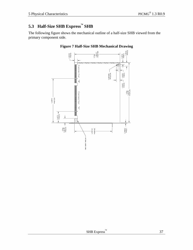
5.3 Half-Size SHB Express™ SHB The following figure shows the mechanical outline of a half-size SHB viewed from the primary component side.
Figure 7 Half-Size SHB Mechanical Drawing

PICMG® 1.3 R0.9 5 Physical Characteristics
SHB Express™
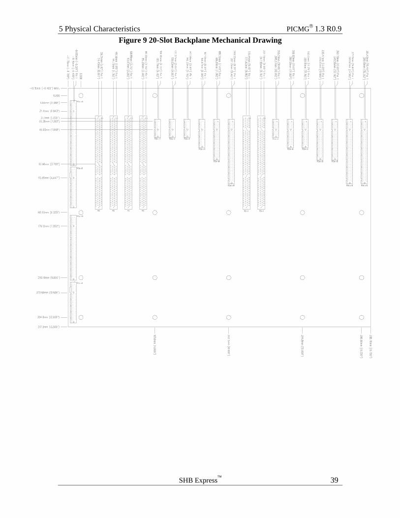
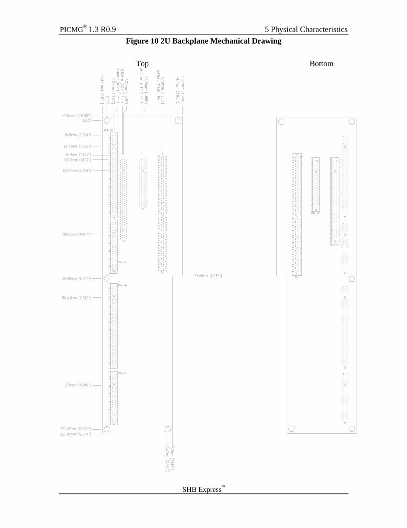
5.4 Backplane Mechanicals A SHB Express™ backplane should follow one of the following mechanical drawings. Note that the PCIe and PCI(-X) connectors seen in Figures 5, 6, and 7 are for illustrative purposes only.
Figure 8 13-Slot Backplane Mechanical Drawing
5 Physical Characteristics PICMG® 1.3 R0.9
SHB Express™ 39
Figure 9 20-Slot Backplane Mechanical Drawing
PICMG® 1.3 R0.9 5 Physical Characteristics
SHB Express™
Figure 10 2U Backplane Mechanical Drawing
Top Bottom

5 Physical Characteristics PICMG® 1.3 R0.9
SHB Express™ 41
This page intentionally left blank.
6 Revision History PICMG® 1.3 R0.9
6 REVISION HISTORY
Revision 0.02 Initial concept. Revision 0.03 Added PCI(-X) and broke x8 PCIe into (1) x4 and (4) x1’s. Revision 0.04 Cleaned up PCI section for Connector D. Defined PCIe split on
Connector A and B more clearly. Revision 0.7 Changed component side of the board to be the non-PCI side of the
SHB. Revision 0.71 Incorporated committee input and changed general format to be
similar to standard PICMG layout. Revision 0.8 Miscellaneous clean-up, changed PCIe link configurations and
added backplane dimensions. Revision 0.81 Updated dimension drawings, simulation information, defined
PCIe clocking more clearly, clarified aux voltages, and miscellaneous clean-up.
Revision 0.9 Updated Connectors A, B, and C pinouts. Removed 2 SATA and replaced with an ethernet connection.


![PCI Express to PCI-X Reversible Bridge · PDF filePCI Express to PCI-X Reversible Bridge Revision 2.5 ... 7.5.135 bit [30] of Replay and ... 6 PCI EXPRESS FUNCTIONAL OVERVIEW](https://static.fdocuments.in/doc/165x107/5ab0dd047f8b9a00728b95ba/pci-express-to-pci-x-reversible-bridge-express-to-pci-x-reversible-bridge-revision.jpg)