SUBSTRATE NOISE FULL-CHIP LEVEL ANALYSIS FLOW FROM EARLY DESIGN STAGES TILL TAPEOUT · SUBSTRATE...
32
SUBSTRATE NOISE FULL-CHIP LEVEL ANALYSIS FLOW FROM EARLY DESIGN STAGES TILL TAPEOUT Hagay Guterman, CSR Jerome Toublanc, Ansys
Transcript of SUBSTRATE NOISE FULL-CHIP LEVEL ANALYSIS FLOW FROM EARLY DESIGN STAGES TILL TAPEOUT · SUBSTRATE...
SUBSTRATE NOISE FULL-CHIP LEVEL
ANALYSIS FLOW FROM EARLY DESIGN
STAGES TILL TAPEOUT
Hagay Guterman, CSR
Jerome Toublanc, Ansys

Hagay Guterman is a senior signal and power integrity engineer at CSR. He has
prior experience as an analogue and circuit designer. He presently works on signal
integrity in highly dense mixed signal ICs inside and outside of the DIE.
Hagay Guterman, CSR
Jerome Toublanc is Principal Product Engineer for ANSYS providing technical
support in Europe and driving the development for Power and Noise solutions for
full System Integrity. Prior experiences focused on physical implementation tools as
well as analog/digital full-custom design.
Jerome Toublanc, Ansys
Speakers
2
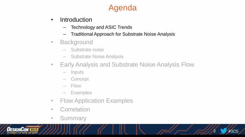
Agenda
• Introduction – Technology and ASIC Trends
– Traditional Approach for Substrate Noise Analysis
• Background – Substrate noise
– Substrate Noise Analysis
• Early Analysis and Substrate Noise Analysis Flow – Inputs
– Concept
– Flow
– Examples
• Flow Application Examples
• Correlation
• Summary
3

Technology Trends
4
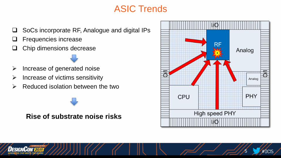
ASIC Trends
SoCs incorporate RF, Analogue and digital IPs
Frequencies increase
Chip dimensions decrease
Increase of generated noise
Increase of victims sensitivity
Reduced isolation between the two
Rise of substrate noise risks
5

Traditional Approach for Substrate Noise Analysis
Jan Feb Apr May Jul Sep
floorplanning
placement
clock tree
routing
extraction
substrate noise simulation
floorplanning 2
placement 2
clock tree 2
routing 2
TapeOut
target
Required: A method to analyze substrate noise earlier
• Relies on final chip design database
• Occurs during the last stages prior
tapeout
• Used for signoff, lessons for next
projects or informational purposes
Jan Feb Apr May Jul Sep
floorplanning
placement
clock tree
routing
extraction
substrate noise simulation
floorplanning 2
placement 2
clock tree 2
routing 2
TapeOut
target
6
Agenda
• Introduction – Technology and ASIC Trends
– Traditional Approach for Substrate Noise Analysis
• Background – Substrate noise
– Substrate Noise Analysis
• Early Analysis and Substrate Noise Analysis Flow – Inputs
– Concept
– Flow
– Examples
• Flow Application Examples
• Correlation
• Summary
7
Package
VDD Dig VDD Ana VSS S1 S2 S3
i
time SoC
Substrate Noise
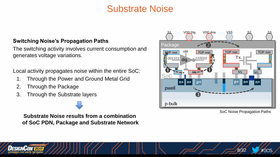
Switching Noise’s Propagation Paths
The switching activity involves current consumption and
generates voltage variations.
Local activity propagates noise within the entire SoC:
1. Through the Power and Ground Metal Grid
2. Through the Package
3. Through the Substrate layers
SoC Noise Propagation Paths
p-bulk
pwell
n+ p+ p+ n+ n+ n+
001101 110010 dig.
vdd
vss M1
V
TOP met
M1
V
TOP met
Tx.
M1 M1 V V
TOP met TOP met
8/32
Substrate Noise results from a combination
of SoC PDN, Package and Substrate Network
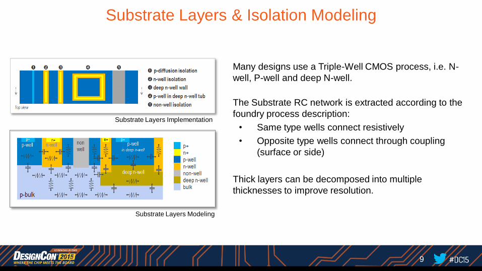
Substrate Layers & Isolation Modeling
Substrate Layers Modeling
Many designs use a Triple-Well CMOS process, i.e. N-
well, P-well and deep N-well.
The Substrate RC network is extracted according to the
foundry process description:
• Same type wells connect resistively
• Opposite type wells connect through coupling
(surface or side)
Thick layers can be decomposed into multiple
thicknesses to improve resolution.
Substrate Layers Implementation
9

Data Inputs
SoC data
- LEF
- DEF
- SPEF
- GDSS
Package data
- layout db
- pre-extracted model
Activity data
- VCD based
- Vectorless + STA
Library data
- Current profiles
- Intrinsic parasitics
Technology rules
Substrate Noise Analysis – SignOff Flow
Results Exploration
Simulation vs. Measurements Voltage Amplitude per Layer
Substrate Weakness Map Point to Point Resistance & Tracing
10
Noise Simulation
-1-
Data Import & Setup
-2-
P/G Grid & Substrate
Extraction
-3-
Power Calculation
-4-
Dynamic Simulation
RedHawk / Totem
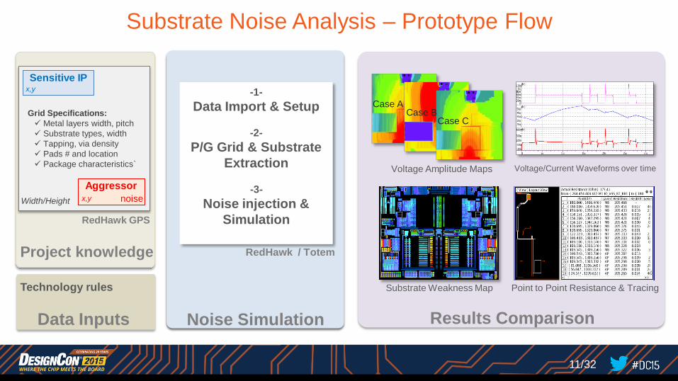
Noise Simulation
-1-
Data Import & Setup
-2-
P/G Grid & Substrate
Extraction
-3-
Power Calculation
-4-
Dynamic Simulation
RedHawk / Totem
Noise Simulation
-1-
Data Import & Setup
-2-
P/G Grid & Substrate
Extraction
-3-
Noise injection &
Simulation
RedHawk / Totem
Substrate Noise Analysis – Prototype Flow
Results Exploration
Simulation vs. Measurements Voltage Amplitude per Layer
Substrate Weakness Map Point to Point Resistance & Tracing
11/32
Data Inputs
Technology rules
Case A Case B Case C
Voltage Amplitude Maps Voltage/Current Waveforms over time
RedHawk GPS
Grid Specifications:
Metal layers width, pitch
Substrate types, width
Tapping, via density
Pads # and location
Package characteristics`
Width/Height x,y noise
Sensitive IP x,y
Aggressor
Project knowledge
Results Comparison

Agenda
• Introduction – Technology and ASIC Trends
– Traditional Approach for Substrate Noise Analysis
• Background – Substrate noise
– Substrate Noise Analysis
• Early Analysis and Substrate Noise Analysis Flow – Chip level analysis inputs
– Early analysis concept
– Flow
– Examples
• Flow Application Examples
• Correlation
• Summary
12
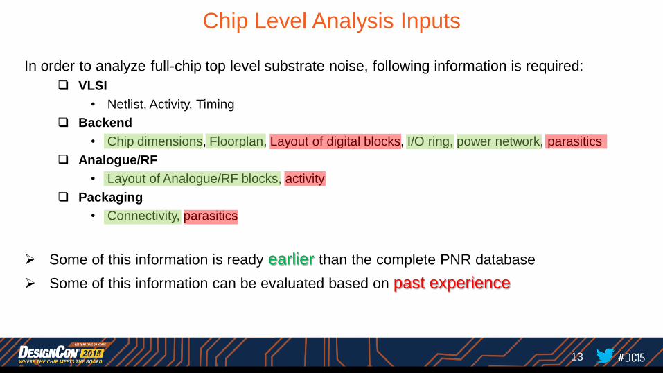
In order to analyze full-chip top level substrate noise, following information is required:
VLSI
• Netlist, Activity, Timing
Backend
• Chip dimensions, Floorplan, Layout of digital blocks, I/O ring, power network, parasitics
Analogue/RF
• Layout of Analogue/RF blocks, activity
Packaging
• Connectivity, parasitics
Some of this information is ready earlier than the complete PNR database
Some of this information can be evaluated based on past experience
Chip Level Analysis Inputs
13
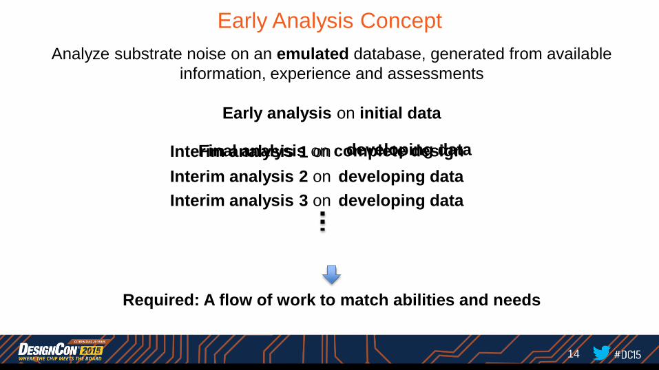
Early Analysis Concept
Required: A flow of work to match abilities and needs
Analyze substrate noise on an emulated database, generated from available
information, experience and assessments
Early analysis on initial data
developing data Interim analysis on
developing data Interim analysis 2 on
developing data Interim analysis 3 on
1
Final analysis on complete design
14
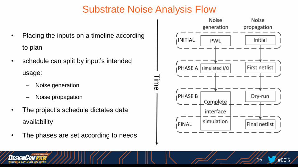
Substrate Noise Analysis Flow
• Placing the inputs on a timeline according
to plan
• schedule can split by input’s intended
usage:
– Noise generation
– Noise propagation
• The project’s schedule dictates data
availability
• The phases are set according to needs T
ime
15
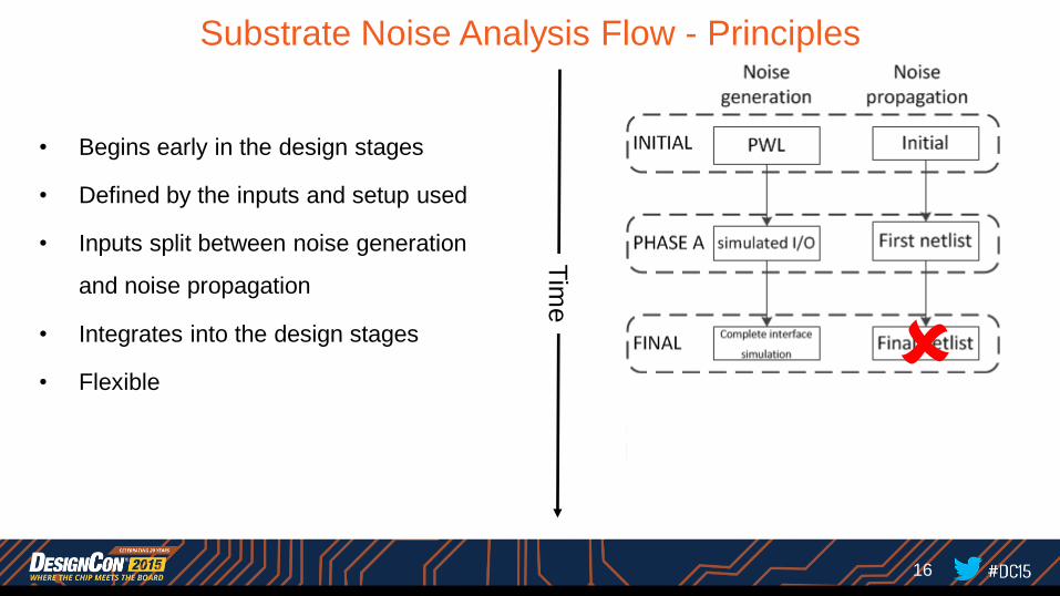
• Begins early in the design stages
• Defined by the inputs and setup used
• Inputs split between noise generation
and noise propagation
• Integrates into the design stages
• Flexible
Substrate Noise Analysis Flow - Principles
Tim
e
16
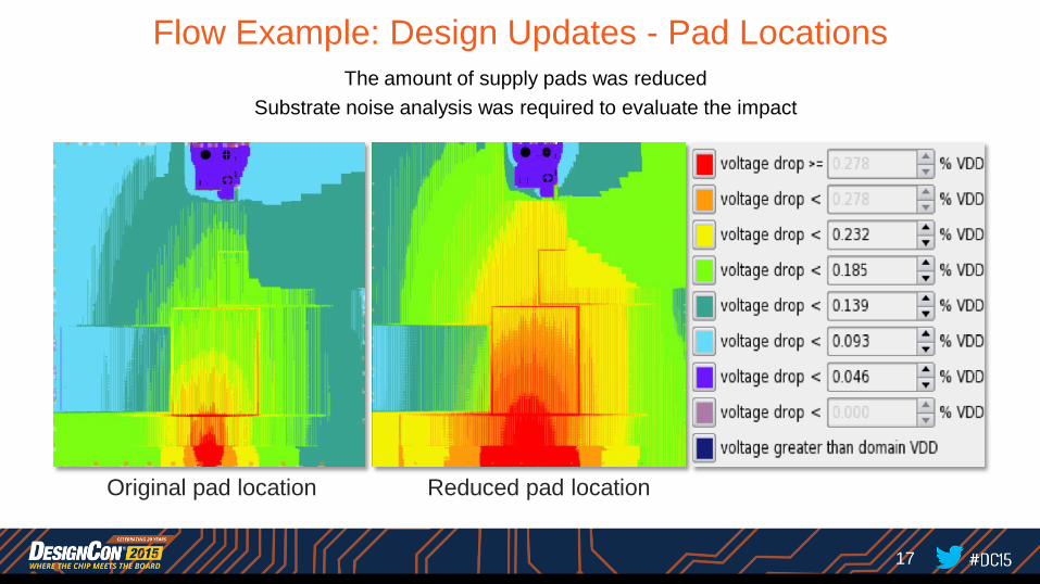
Flow Example: Design Updates - Pad Locations
The amount of supply pads was reduced
Substrate noise analysis was required to evaluate the impact
Original pad location Reduced pad location
17
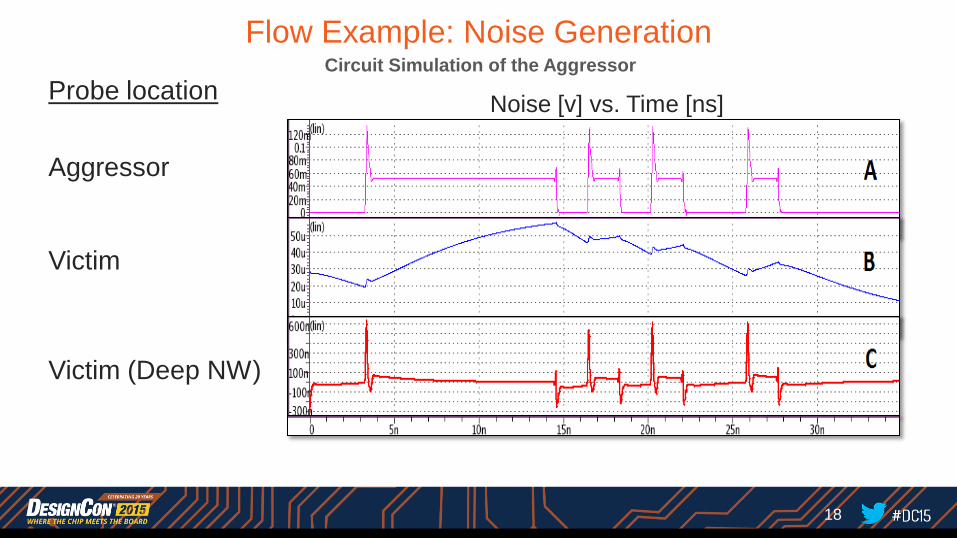
Flow Example: Noise Generation
Probe location
Aggressor
Victim
Victim (Deep NW)
Circuit Simulation of the Aggressor
Noise [v] vs. Time [ns]
18
Agenda
• Introduction – Technology and ASIC Trends
– Traditional Approach for Substrate Noise Analysis
• Background – Substrate noise
– Substrate Noise Analysis
• Early Analysis and Substrate Noise Analysis Flow – Inputs
– Concept
– Flow
– Examples
• Flow Application Examples
• Correlation
• Summary
19

Flow Applications
• Substrate noise related fixes and design alternatives require changes in – Aggressor
– Floorplan
– Isolation
– Layout
– Activity
• Modifications in these design elements are costly
• Solution: Using the technique of the flow (emulated database) – Implementing alternative designs without modifying the real design
– Evaluating the optional modifications
– Validating expected trends
20
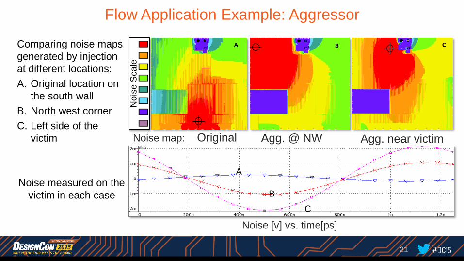
Flow Application Example: Aggressor
Comparing noise maps
generated by injection
at different locations:
A. Original location on
the south wall
B. North west corner
C. Left side of the
victim
Noise measured on the
victim in each case
A
B
C
Noise [v] vs. time[ps]
Noise map: Original Agg. @ NW Agg. near victim N
ois
e S
cale
21

Flow Application Example: Floorplan
Comparing substrate
noise between two
floorplans:
• RF victim is on the
north wall
• RF victim is on the
east wall
Original IP location
Noise map
IP moved to east wall
Noise map
Nois
e S
cale
22
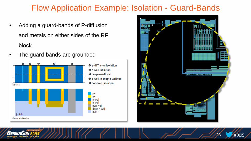
Flow Application Example: Isolation - Guard-Bands
• Adding a guard-bands of P-diffusion
and metals on either sides of the RF
block
• The guard-bands are grounded
23

Flow Application Example: Isolation - Guard-Bands - Results
Original design
Noise map
Addition of side guard bands
Noise map
• Effects can be
observed both inside
and outside of the
victim
• Alternative ring
architectures may be
easily implemented
and compared
Nois
e S
ca
le
24
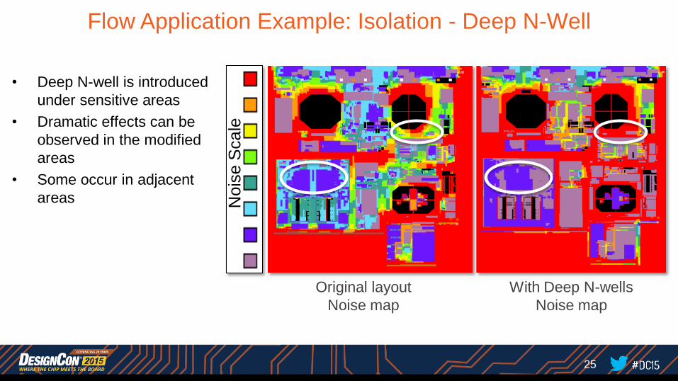
Flow Application Example: Isolation - Deep N-Well
• Deep N-well is introduced
under sensitive areas
• Dramatic effects can be
observed in the modified
areas
• Some occur in adjacent
areas
Original layout
Noise map
With Deep N-wells
Noise map
Nois
e S
ca
le
25
Agenda
• Introduction – Technology and ASIC Trends
– Traditional Approach for Substrate Noise Analysis
• Background – Substrate noise
– Substrate Noise Analysis
• Early Analysis and Substrate Noise Analysis Flow – Inputs
– Concept
– Flow
– Examples
• Flow Application Examples
• Correlation
• Summary
26
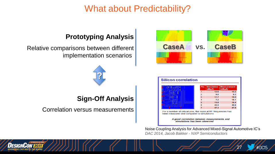
What about Predictability?
Prototyping Analysis
Relative comparisons between different
implementation scenarios
CaseA vs. CaseB
Sign-Off Analysis
Correlation versus measurements
Noise Coupling Analysis for Advanced Mixed-Signal Automotive IC’s
DAC 2014, Jacob Bakker - NXP Semiconductors
?
27
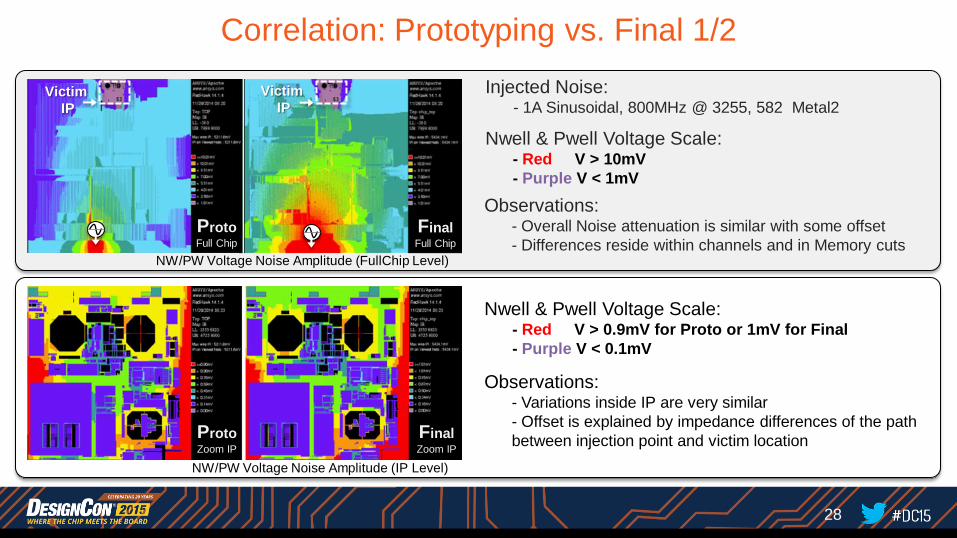
Correlation: Prototyping vs. Final 1/2
NW/PW Voltage Noise Amplitude (FullChip Level)
Nwell & Pwell Voltage Scale: - Red V > 10mV
- Purple V < 1mV
Injected Noise: - 1A Sinusoidal, 800MHz @ 3255, 582 Metal2
Observations: - Overall Noise attenuation is similar with some offset
- Differences reside within channels and in Memory cuts
Nwell & Pwell Voltage Scale: - Red V > 0.9mV for Proto or 1mV for Final
- Purple V < 0.1mV
Observations: - Variations inside IP are very similar
- Offset is explained by impedance differences of the path
between injection point and victim location Proto Zoom IP
Final Zoom IP
NW/PW Voltage Noise Amplitude (IP Level)
Proto Full Chip
Victim
IP
Victim
IP
Final Full Chip
28

Proto Zoom IP
Final Zoom IP
Correlation: Prototyping vs. Final 2/2
A A B B
E E C C
D D
PW’s Voltage Waveforms over time
Probes inside victim IP from Prototype db Probes inside victim IP from Final db
29
Agenda
• Introduction – Technology and ASIC Trends
– Traditional Approach for Substrate Noise Analysis
• Background – Substrate noise
– Substrate Noise Analysis
• Early Analysis and Substrate Noise Analysis Flow – Inputs
– Concept
– Flow
– Examples
• Flow Application Examples
• Correlation
• Summary
30
Summary
• Early Substrate analysis
– Often required
– Depends on input quality and design knowledge
– Reliable based on correlation
• Flow
– Accommodate to the project’s schedule
– Flexible
• Method (emulated database)
– “Cheap” evaluation of alternative designs
31
Thank you
32