Tapeout Documentation
8
Testing of Radiation Hardened Transistors Made in Jazz 0.18μm process The tape-out features radiation hardened transistors and also some sample test circuit structures laid out for ready performance assessment and in comparison to conventional transistors. Goal of this documentation is to help test engineer understand what pins need to be probed or powered for successful testing of each of these test circuits. Circuits: transistor arrays, ring osc illators, a flip-flop and some transmission gates. 2011 Vedhas Sadanand Pandit Email: [email protected] 6/21/2011
-
Upload
whosthishere -
Category
Documents
-
view
220 -
download
0
Transcript of Tapeout Documentation

8/6/2019 Tapeout Documentation
http://slidepdf.com/reader/full/tapeout-documentation 1/7
Testing of RadiationHardened TransistorsMade in Jazz 0.18μm process
The tape-out features radiation hardened transistors and also some sample test
circuit structures laid out for ready performance assessment and in comparison to
conventional transistors. Goal of this documentation is to help test engineer
understand what pins need to be probed or powered for successful testing of
each of these test circuits. Circuits: transistor arrays, ring oscillators, a flip-flop and
some transmission gates.
2011
Vedhas Sadanand Pandit
Email: [email protected]
6/21/2011

8/6/2019 Tapeout Documentation
http://slidepdf.com/reader/full/tapeout-documentation 2/7
2 | P a g e
Table of Contents
Tapeout overview ............................................................. 3
Pin-number to pin-name correspondence ....................... 4
Circuit descriptions and pin connections .......................... 4
Power connections .................................................... 4
Ring oscillators ........................................................... 4
Transistor Test Structures .......................................... 6
Bipolar Test Structure ................................................ 7
D flip flop ................................................................... 7
Transmission gates .................................................... 7
8/6/2019 Tapeout Documentation
http://slidepdf.com/reader/full/tapeout-documentation 3/7
3 | P a g e
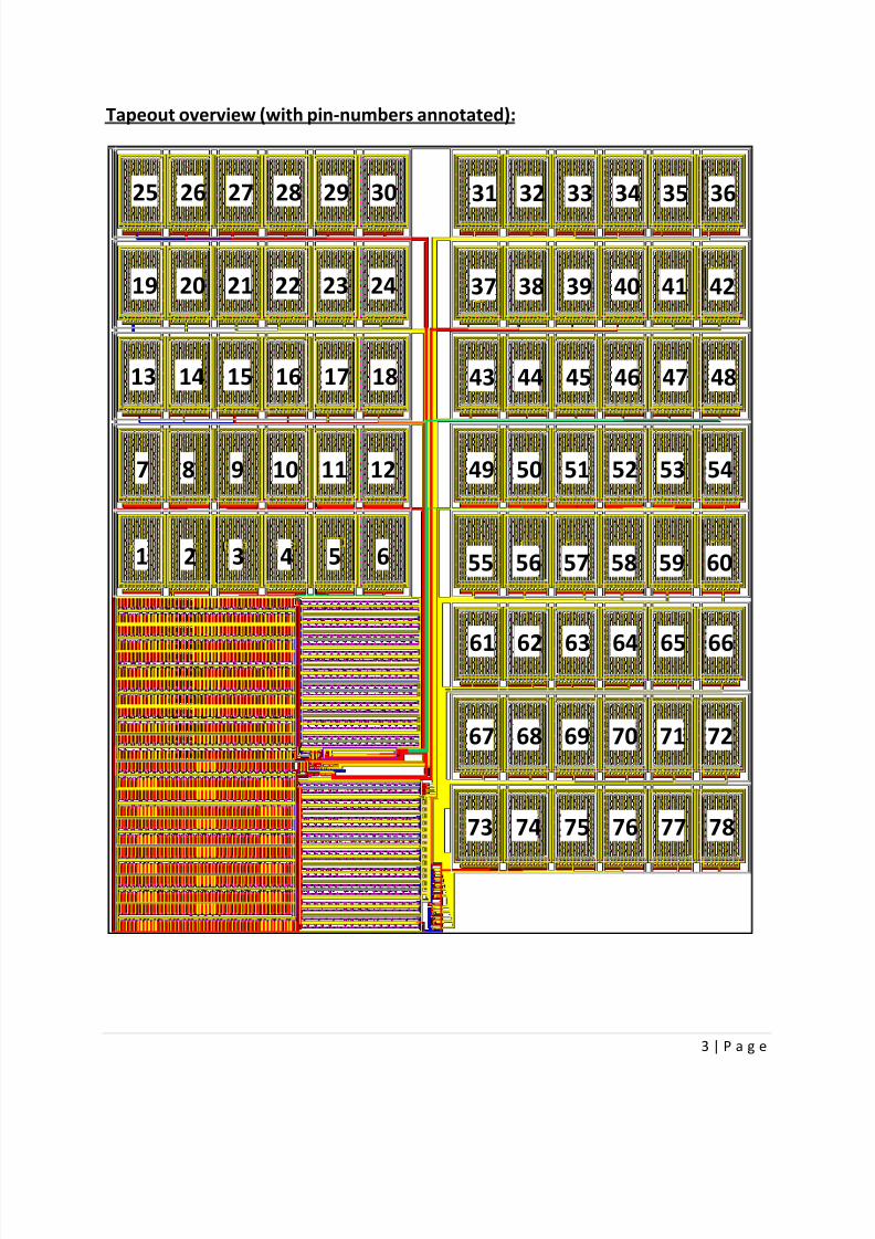
Tapeout overview (with pin-numbers annotated):
1 2 3 4 5 6
7 8 9 10 11 12
13 14 15 16 17 18
19 20 21 22 23 24
25 26 27 28 29 30
43 44 45 46 47 48
37 38 39 40 41 42
31 32 33 34 35 36
55 56 57 58 59 60
49 50 51 52 53 54
73 74 75 76 77 78
67 68 69 70 71 72
61 62 63 64 65 66

8/6/2019 Tapeout Documentation
http://slidepdf.com/reader/full/tapeout-documentation 4/7
4 | P a g e
Pin-number to pin-name correspondence:
1 dsub 2 dgnd 3 dvdd 4 dvnw 5 Out1LR 6 Out1SR
7 Out1SN 8 Out1LN 9 Out2SR 10 Out2LR 11 Out2SN 12 Out2LN
13 GLN 14 DLN1 15 DLN2 16 DLN3 17 DLN4 18 DLN5
19 GSN 20 DSN1 21 DSN2 22 DSN3 23 DSN4 24 DSN5
25 GSR 26 DSR1 27 DSR2 28 DSR3 29 DSR4 30 DSR5
31 GLR 32 DLR1 33 DLR2 34 DLR3 35 DLR4 36 DLR5
37 GP 38 DP1 39 DP2 40 DP3 41 Base2 42 Emitter2
43 Emitter1 44 Base1 45 pre 46 d 47 clr 48 clk
49 qb 50 q 51 N 52 P 53 A4 54 B4
55 A2p5 56 B2p5 57 A2 58 B2 59 A1p5 60 B1p5
61 A1 62 B1 63 Ap5 64 Bp5 65 B4E 66 A4E
67 A3E 68 B3E 69 A2p5E 70 B2p5E 71 A2E 72 B2E
73 A3 74 B3 75 A1p5E 76 B1p5E 77 A1E 78 B1E
Circuit descriptions and pin connections:
Power connections (4 pins):
dsub: Sets the substrate voltage. Body tie for all nmos, common collector of all bipolars.
dgnd: Ground connection. Sources of nmos’s in ring oscillators are shorted to this pin.
dvdd: Vdd connection. Sources of pmos’s in ring oscillators are shorted to this pin.
dvnw: Sets the nwell voltage. Body tie for all pmos in the circuit.
Ring oscillators (2 x 4 = 8 output pins):
There are four ring oscillators in the circuit. Each of the ring oscillators has 577 inverter stages,
followed by an output buffer in order to avoid possible loading of the oscillator circuit. Every
output stage buffer is made of two inverters, and the inverters are identical to the ones used in
preceding ring oscillator circuit. Output for the oscillator part alone is given to the pin with a
name that is prefixed with ‘Out1’ while output from the buf fer stage is given to the pin with a
name prefixed with ‘Out2’. Suffixes in the name denote type of ring oscillator: L/S for indicating
whether a large (L) or small (S) nmos is used, N/R to indicate whether Radiation hardened (N) or
Regular (R) nmos is used.
Out1xx
Out2xx

8/6/2019 Tapeout Documentation
http://slidepdf.com/reader/full/tapeout-documentation 5/7
5 | P a g e
Therefore, we have:
and nmos is radiation hardened nmos, having two fingers each 10μm wide.
and nmos is radiation hardened nmos, having two fingers each 0.5μm wide.
and nmos in use is regular ca18 library nmos, having two fingers each 10μm wide.
and nmos in use is regular ca18 library nmos, having two fingers each 0.5μm wide.
For all these circuits, pmos have six 5μm-wide fingers.
Out1LN
Out2LN
Out1SN
Out2SN
Out1LR
Out2LR
Out1SR
Out2SR
8/6/2019 Tapeout Documentation
http://slidepdf.com/reader/full/tapeout-documentation 6/7
6 | P a g e
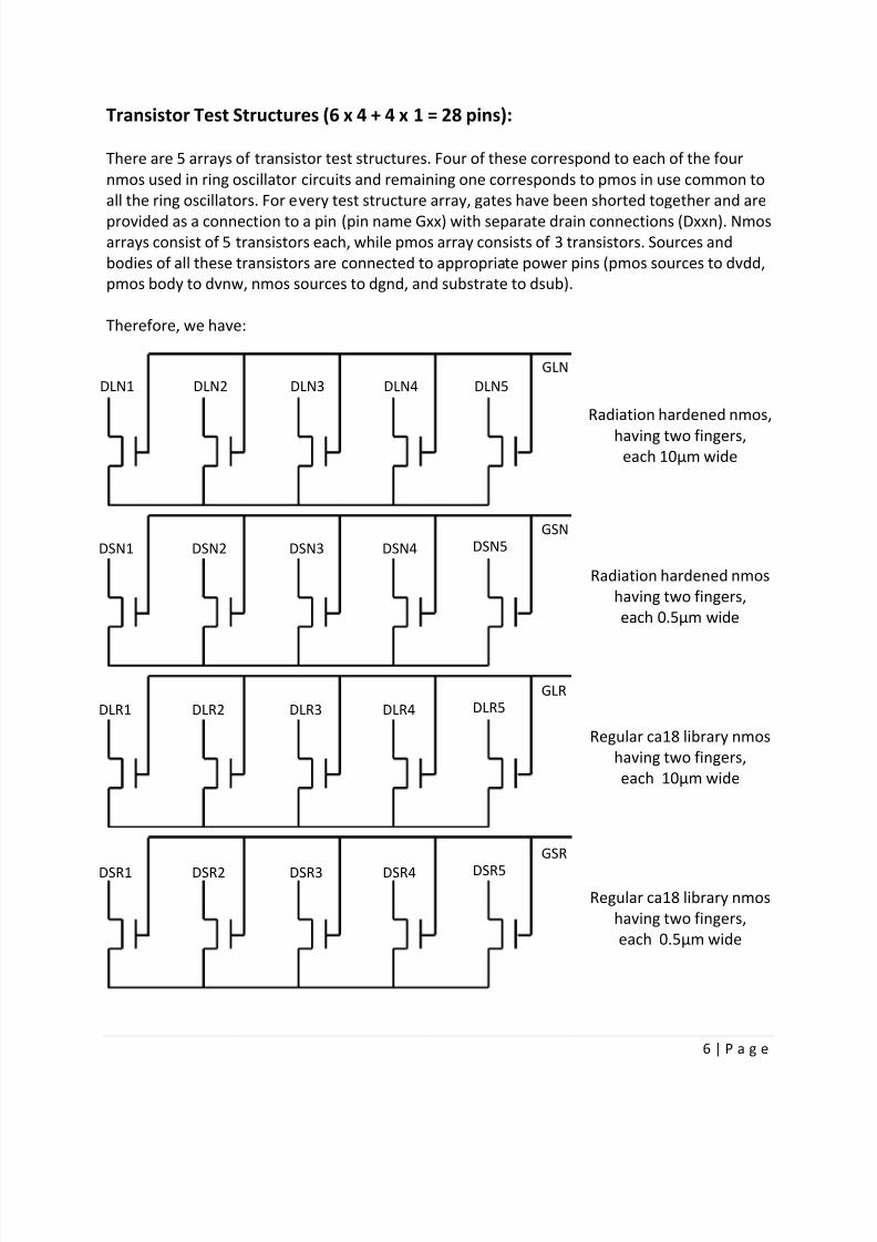
Transistor Test Structures (6 x 4 + 4 x 1 = 28 pins):
There are 5 arrays of transistor test structures. Four of these correspond to each of the four
nmos used in ring oscillator circuits and remaining one corresponds to pmos in use common to
all the ring oscillators. For every test structure array, gates have been shorted together and are
provided as a connection to a pin (pin name Gxx) with separate drain connections (Dxxn). Nmosarrays consist of 5 transistors each, while pmos array consists of 3 transistors. Sources and
bodies of all these transistors are connected to appropriate power pins (pmos sources to dvdd,
pmos body to dvnw, nmos sources to dgnd, and substrate to dsub).
Therefore, we have:
Radiation hardened nmos,
having two fingers,each 10μm wide
Radiation hardened nmos
having two fingers,
each 0.5μm wide
Regular ca18 library nmos
having two fingers,
each 10μm wide
Regular ca18 library nmos
having two fingers,
each 0.5μm wide
DLR1 DLR2 DLR3 DLR4 DLR5GLR
DSR1 DSR2 DSR3 DSR4 DSR5
GSR
DLN1 DLN2 DLN3 DLN4 DLN5
GLN
DSN1 DSN2 DSN3 DSN4 DSN5GSN

8/6/2019 Tapeout Documentation
http://slidepdf.com/reader/full/tapeout-documentation 7/7
7 | P a g e
Regular ca18 library pmos,
six fingers each 5μm wide
Bipolar Test Structure (4 x 1 = 4 pins):
Following schematic has been laid out with pin-names as noted. The common collector terminal
is connected to dsub pin.
D flip flop (6 x 1 = 6 pins):
Input pin Description
d D Inputclk Clock input
pre Pre-charge input
clr Clear input
q Q output
qb Qb output
Transmission gates (2 + 2 x 13 = 28 pins):
Transmission gates have pin-name correspondence
as shown in the adjoining figure. N & P pins have
been shorted for all the tgates. The ‘size’ parameter
indicates width of nmos finger. Because each of the
Radiation hardened nmos uses 2 fingers, width of
nmos =2 x size x 100 μm. Presence/absence of letter
E indicates whether or not ‘enclosed’ (radiation
hardened) pmos is used for the corresponding
tgate. All the transistors have gate length = 180nm.
Emitter1
Base1
Emitter2
Base2
dsub
DP1 DP2 DP3GP