Performance Substrate Technology for Automotive ... Substrate...Performance Substrate Technology for...
52
Performance Substrate Technology for Automotive Applications Utilizing DPC and SuperMCPCB Technology Performance Substrate Technology for Automotive Applications Utilizing DPC and SuperMCPCB Technology Presented by: Heinz Ru Date: April 28 th , 2010 Presented by: Heinz Ru Date: April 28 th , 2010
Transcript of Performance Substrate Technology for Automotive ... Substrate...Performance Substrate Technology for...

Performance Substrate Technology for Automotive Applications
Utilizing DPC and SuperMCPCBTechnology
Performance Substrate Technology for Automotive Applications
Utilizing DPC and SuperMCPCBTechnology
Presented by: Heinz RuDate: April 28th , 2010
Presented by: Heinz RuDate: April 28th , 2010

High Thermal Demand Packaging for Automotive Applications
Motor Control Circuits
High BrightnessLEDs

Automotive Motor ControlAutomotive Motor Control
• High intensity discharge headlamp control module
• Ignition modules
• Air flow sensors
• Fan control module
• A/C control module
• Starter motors
• Voltage regulators
• Fuel level sensors
• Hybrid cars- electric motor control

HBLED in Automotive ApplicationsHBLED in Automotive Applications
• Headlamps
• Signal Lighting
• Tail Lamps
• Interior Lighting
• Display Backside Illumination

Technology Driver for Motor Control and HBLED Usage in Automotive
Applications: Improved Fuel Economy
Technology Driver for Motor Control and HBLED Usage in Automotive
Applications: Improved Fuel Economy

Power Density of Various High Power Semiconductor DevicesPower Density of Various High Power Semiconductor Devices
HBLED and Power Semiconductors dissipate high power
Source: CMC Interconnect Technologies, 2008

HBLED Packaging Requirements
HBLED Packaging Requirements

HBLED Power TrendsHBLED Power Trends
Thermal Management will continue to be a key aspect of HBLED packagingThermal Management will continue to be a key aspect of HBLED packaging
Source: Scott Kern and Markus Maile, Philips Lumileds Lighting, IESNA Buffalo, NY

HBLED Light Flux Output vs. TimeHBLED Light Flux Output vs. Time

Effect of LED Junction Temperature on Device Lifetime
Effect of LED Junction Temperature on Device Lifetime
Lower the LED operating temperatures mean longer the device lifetime. This illustrates the critical role of packaging in efficient heat removal.Lower the LED operating temperatures mean longer the device lifetime. This illustrates the critical role of packaging in efficient heat removal.
Source: Data from Philips Lumileds

Effect of Rj-a on LED PerformanceEffect of Rj-a on LED Performance
Rj-a is the thermal resistance from the device junction to ambient. The package is a major contributor to lowering Rj-a. Note the impact on device efficacy (amount of light per power input)
Rj-a is the thermal resistance from the device junction to ambient. The package is a major contributor to lowering Rj-a. Note the impact on device efficacy (amount of light per power input)
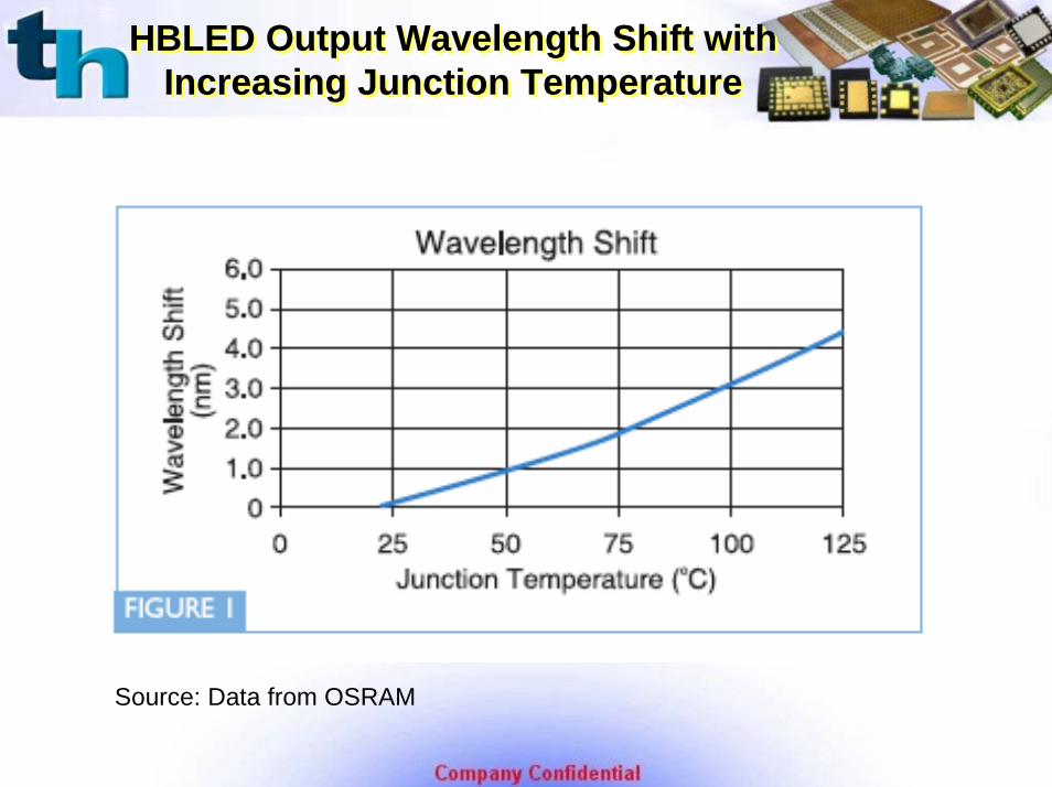
HBLED Output Wavelength Shift with Increasing Junction Temperature
HBLED Output Wavelength Shift with Increasing Junction Temperature
Source: Data from OSRAM

To Summarize….To Summarize….
• HBLED devices generate power densities up to 500 Watts/cm2!!
• HBLED light output degrades as the device temperature increases
• HBLED lifetime degrades as the device temperature increases
• HBLED power will continue to increase
• The HBLED package is the only thermal pathway for heat dissipation
• Thermal management is a critical requirement for HBLED packaging

In Addition….In Addition….
• HBLED packages must be low cost since market growth is driven by consumer and automotive applications
• HBLED packages must be manufacturable in very high volumes
• HBLED packages must be suitable for high volume, automated assembly

Power Semiconductor Packaging Requirements
Power Semiconductor Packaging Requirements

Power Semiconductor ModulesPower Semiconductor Modules
• Switch and control extremely high electrical currents (300 A)
• Modules can operate at voltages as high as 600V
• Power densities as high as 200 W/cm2

Packaging for Automotive Power Semiconductor Modules
Packaging for Automotive Power Semiconductor Modules
• Very high current carrying capability
• High dielectric breakdown voltage materials
• High thermal dissipation
• Manufacturable in high volumes at low costs
• Suitable for high volume automated assembly
• Mechanically rugged
• High reliability

Reliability Requirements for Automotive Applications
Reliability Requirements for Automotive Applications
• High Temperature stability- up to 150C continuous operation for under-hood applications
• 2000 temperature cycle -50 to +150C
• 1000 hours at 85C/85% RH with 14 V bias
• Harsh vibration resistance
• Acceleration tolerance
• Harsh environmental requirements

Direct Plated Copper (DPC)Direct Plated Copper (DPC)
Key Attributes Direct Plated Copper (DPC) Technology
Key Attributes Direct Plated Copper (DPC) Technology
• Unsurpassed thermal performance
• Low electrical resistance conductor lines
• Stable up to temperatures >340°C
• Accurate feature location, compatible with automated, large format assembly
• Fine line resolution allowing high density of devices and circuitry
• Proven reliability
• Mechanically rugged ceramic construction
• Lowest cost, highest performance ceramic solution

DPC Technology is Field- Proven in High Thermal Demand ApplicationsDPC Technology is Field- Proven in High Thermal Demand Applications
• High Brightness LEDs
• Power Semiconductors
• RF and Microwave Devices
• Dense Memory Stacks

Description of DPC TechnologyDescription of DPC Technology
• Base substrate: Al2O3 or AlN
• Proprietary base metallization for robust metallizationadhesion
• Laser drilled vias down to 50μm and filled with dense, plated Cu
• Thick plated copper lines and pads up to 100μm thick
• Photolithographic patterning
• Plated Ni, Au surface metal

DPC: Two Ceramic Options Depending on Thermal Design
DPC: Two Ceramic Options Depending on Thermal Design

DPC Construction- Plan ViewDPC Construction- Plan View

DPC Construction- Plan ViewDPC Construction- Plan View

DPC Construction - Cross Sections
DPC Construction - Cross Sections

Copper Thermal Conductivity Compared with Other Ceramic Metallization MaterialsCopper Thermal Conductivity Compared
with Other Ceramic Metallization Materials
Copper has far superior thermal and electrical properties compared to other ceramic metallization
Copper has far superior thermal and electrical properties compared to other ceramic metallization

Proprietary Bonding LayerProprietary Bonding Layer
Thick Plated Cu Layer
Proprietary Bonding Layer
Proprietary Bonding Layer
Substrate
2 µm scale

DPC Metal AdhesionDPC Metal Adhesion

DPC Metallization AdhesionDPC Metallization Adhesion
Alumina ceramic
Peeled CuDPC metal adhesion is stronger than the ceramic substrate

DPC-Large Format SizeDPC-Large Format Size
• Format size up to 4” x 4”
• High feature location accuracy across the entire substrate
• Compatible with automated assembly

DPC Design FlexibilityDPC Design Flexibility
• Wide range of plated metallization layers can be used
• Soft tooled factory, low NRE for new designs
• Ceramic thicknesses from 10-100 mils
• Cu thicknesses up to 4 mils
• Via holes sizes from 2 mils to 20 mils or larger
• Alumina or ALN ceramic substrates

Low CostLow Cost
• High throughput manufacturing
• Automated high volume Cu rack plating line
• Process developed for low cost ceramic substrates (thick film grade)
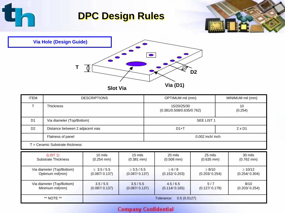
DPC Design RulesDPC Design Rules
Via Hole (Design Guide)
T
Via (D1) Slot Via
D2
ITEM DESCRIPTIONS OPTIMUM mil (mm) MINIMUM mil (mm)
T Thickness 15/20/25/30(0.381/0.508/0.635/0.762)
10(0.254)
D1 Via diameter (Top/Bottom) SEE LIST 1
D2 Distance between 2 adjacent vias D1+T 2 x D1
Flatness of panel ≦0.002 inch/ inch
T = Ceramic Substrate thickness
(LIST 1)Substrate Thickness
10 mils(0.254 mm)
15 mils(0.381 mm)
20 mils(0.508 mm)
25 mils(0.635 mm)
30 mils(0.762 mm)
Via diameter (Top/Bottom)Optimum mil(mm)
≥ 3.5 / 5.5(0.087/ 0.137)
≥ 3.5 / 5.5(0.087/ 0.137)
≥ 6 / 8(0.152/ 0.203)
≥ 8/10(0.203/ 0.254)
≥ 10/12(0.254/ 0.304)
Via diameter (Top/Bottom)Minimum mil(mm)
3.5 / 5.5(0.087/ 0.137)
3.5 / 5.5(0.087/ 0.137)
4.5 / 6.5(0.114/ 0.165)
5 / 7(0.127/ 0.178)
8/10(0.203/ 0.254)
** NOTE ** Tolerance: ± 0.5 (0.0127)

DPC Design RulesDPC Design Rules
g
ITEM DESCRIPTIONS OPTIMUMmil (mm)
MINIMUM mil (mm)
a Via Diameter (Top/Bottom)
4.0/6.0(0.101/0.152) -----
b Via pad ----- a+8 (diameter)
c Spacing between circumference around vias 4.0 (0.101) 3.0 (0.076)
d Conductor Width 4.0 (0.101) 3.0 (0.076)
e Clearance between two adjacent traces 4.0 (0.101) 3.0 (0.076)
f Clearance of trace toedge of ceramic 8.0 (0.203) 5.0 (0.127)
g Space between via and donut pattern ----- a+4 (radius)
Trace Dimensions (Design Guide)

Comparison to Competing MaterialsComparison to Competing Materials
Ceramic System
Metal Thermal Conductivity (W/m-K)
Ceramic Thermal Conductivity (W/m-K)
Dimensional Control
Typical Largest Format Size
Cost
DPC 400 20-190 +/- 0.1% of dimension*
4” x 4” Low
HTCC 52-138 20 +/- 0.5% of dimension*
4” x 4” Medium to high
Co-fired AlN 174 170 +/- 0.5% of dimension*
4” x 4” High
Co-fired ceramic tolerance is +/- 0.5% of the distance from the center of the substrate to the feature of interest. For example, the corner of a 3” x 3” substrate would have location tolerance of +/- 10mils

DPC Compared to Competing Multi-Layer Ceramic Options
DPC Compared to Competing Multi-Layer Ceramic Options
• Much higher dimensional tolerance allowing automated assembly and large format
• Much higher thermal and electrical performance metallization
• Equivalent thermal and mechanical ceramic performance
• Lower cost

DPC Compared to DBCDPC Compared to DBC
• DPC forms a true chemical bond between the Cu metallizationlayer and ceramic
• Bond is stronger than the strength of the ceramic
• Higher bond strength than DBC
• DPC technology applies Cu through electro-plating
• Cu can have a wide range of thicknesses from extremely thick for current carrying ability to very thin for fine lines and features
• Excellent electrical and thermal contact between copper plated vias and surface metallization
• Lower temperature processing which means much reduced residual stress in the copper metallization layers and copper/substrate interface

DPC for Automotive Applications -Summary
DPC for Automotive Applications -Summary
• DPC is an ideal packaging material for Motor Control and HBLED used in automotive applications
• Copper with ceramic for unsurpassed thermal performance
• True chemical bonding between packaging materials for improved thermal performance, mechanical ruggedness and reliability
• Design flexibility which allows fine lines, wide range of copper thicknesses and soft-tool driven patterning
• Large format production (4.5” x 4.5”) with precise feature location for low cost automated assembly
• Proven technology in volume production today

DPC Substrates in Combination with SuperMCPCB Boards
DPC Substrates in Combination with SuperMCPCB Boards

Anatomy of SuperMCPCBAnatomy of SuperMCPCB
Conventional MCPCB SuperMCPCB
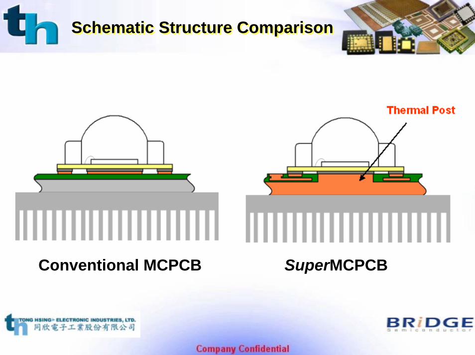
Schematic Structure ComparisonSchematic Structure Comparison
Conventional MCPCB SuperMCPCB

SuperMCPCB Cross Sectional View SuperMCPCB Cross Sectional View
Multiple metal posts for excellent thermal dissipation and reliability
Multi circuitry layers for high-density routing

Key Benefits of SuperMCPCBKey Benefits of SuperMCPCB
• Enhanced Performances • Allow higher forward current (I.e., higher power)
applications due to lower thermal resistance• Higher design flexibility
• Improved Reliability• Mechanically robust structure• No dielectric/metal delamination underneath LEDs
• Competitive Cost• Standard materials• Existing manufacturing infrastructure

Thermal Measurement Set up & Reliability Performances
Thermal Measurement Set up & Reliability Performances
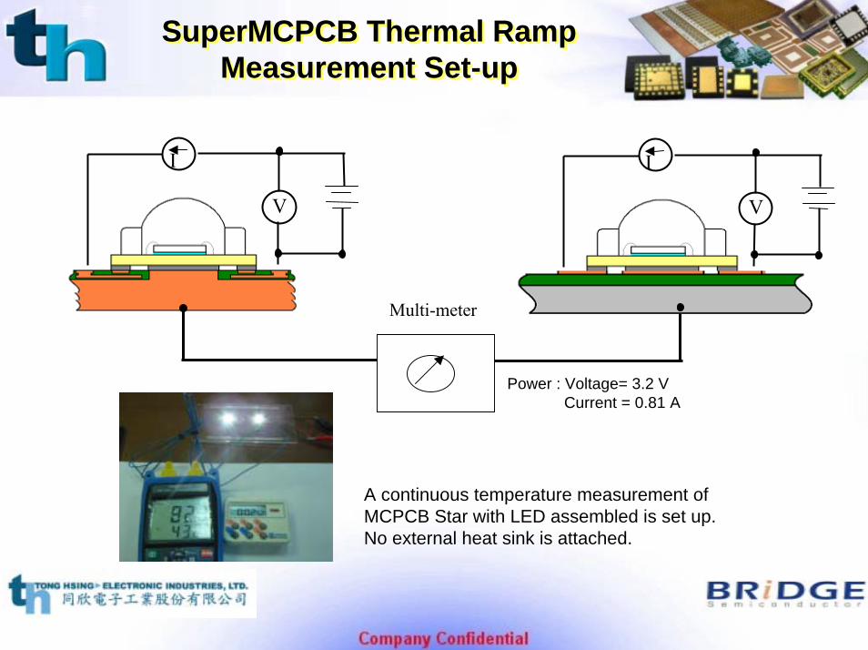
SuperMCPCB Thermal Ramp Measurement Set-up
SuperMCPCB Thermal Ramp Measurement Set-up
Multi-meter
V
I
V
I
Power : Voltage= 3.2 VCurrent = 0.81 A
A continuous temperature measurement of MCPCB Star with LED assembled is set up. No external heat sink is attached.

Transient Thermal Performance Comparison
Transient Thermal Performance Comparison
The diagram shows that the temperature of SuperMCPCB rises quickly and exhibits much lower thermal resistance compared to that of conventional MCPCB.

Compatibility between DPC and SuperMCPCBCompatibility between DPC and SuperMCPCB
SuperMCPCB
Reliability Testing Test Samples Test Results
Thermal Cycle -65 ℃ ~ 150 ℃1000Cycles
SuperSTAR+AlN 15mil All 15 units passed
SuperSTAR +AlN 20mil All 15 units passed
SuperSTAR+Al2O3 20mil All 15 units passed
Thermal Shock -65 ℃~ 150℃ 1000Cycles
SuperSTAR +AlN 15mil All 15 units passed
SuperSTAR +AlN 20mil All 15 units passed
SuperSTAR+Al2O3 20mil All 15 units passed
High Temp Storage +85 ℃/ 5%RH 1000 hrs
SuperSTAR +AlN 15mil All 15 units passed
SuperSTAR +AlN 20mil All 15 units passed
SuperSTAR+Al2O3 20mil All 15 units passed
AlN or Al2O3 substrateSubstrate Sample
Assembly
Reliability Testing
Inspection
Data /Report

Result of Thermal Resistance Measurement
Result of Thermal Resistance Measurement
Group Test Samples Rth of DPC substrate + MCPCB (K/W)
A SuperSTAR + AlN 15mil 2.30
B SuperSTAR + AlN 20mil 2.47
C SuperSTAR + Al2O3 20mil 3.87
D Conventional STAR + AlN 15mil 3.57
E Conventional STAR + AlN 20mil 3.81
F Conventional STAR + Al2O3 20mil 5.16

Key Findings for DPC Substrates (1)Key Findings for DPC Substrates (1)
• Using the same SuperSTAR thermal board, the result showed that by replacing 20 mils metallized Al2O3 substrate with 20 mils metallized AlN, the thermal resistance significantly improved by 1.4 K/W. Mostly because the thermal conductivity of AlN (170 W/mK) is much higher than that of Al2O3 (~24 W/mK).
• The thermal resistance further decreased by 0.24K/W when reducing the thickness of AlN ceramic substrate from 20 to 15 mils.
# Test Sample Combination Rth
A SuperSTAR +AlN 15mil 2.30
B SuperSTAR +AlN 20mil 2.47
C SuperSTAR + Al2O3 20mil 3.87

Key Findings for DPC Substrates (2)Key Findings for DPC Substrates (2)
• Similar trend was obtained in the case of using conventional STAR. By comparing 20 mils of metallized AlN and Al2O3 substrates, the thermal resistance decreased from 5.16 to 3.81 K/W by 1.35 K/W.
• The thermal resistance further decreases to 0.17K/W when reducing the thickness of AlN metallized substrate from 20 to 15 mils.
# Test Sample Combination Rth
D Conventional STAR+AlN 15mil 3.57
E Conventional STAR+AlN 20mil 3.81
F Conventional STAR+Al2O320mil 5.16

Summary: SuperMCPCB in Combination with DPC
Summary: SuperMCPCB in Combination with DPC
• SuperMCPCB offers significantly improved thermal performance when compared to conventional MCPCB technology
• SuperMCPCB can be combined with DPC substrate technology for high thermal demand applications such as HBLED
• Experiments have illustrated 50% decrease in Rthwhen compared to conventional packaging technology