STRUCTURAL OPTIMIZATION & RELIABILITY OF 3D PACKAGE BY ...
90
i STRUCTURAL OPTIMIZATION & RELIABILITY OF 3D PACKAGE BY STUDYING CRACK BEHAVIOR ON TSV & BEOL & IMPACT OF POWER CYCLING ON RELIABILITY FLIP CHIP PACKAGE By UNIQUE RAHANGDALE Presented to the Faculty of the Graduate School of The University of Texas at Arlington in Partial Fulfillment of the Requirements for the Degree of MASTER OF SCIENCE IN MECHANICAL ENGINEERING THE UNIVERSITY OF TEXAS AT ARLINGTON May 2017
Transcript of STRUCTURAL OPTIMIZATION & RELIABILITY OF 3D PACKAGE BY ...
i
STRUCTURAL OPTIMIZATION & RELIABILITY OF 3D PACKAGE BY STUDYING
CRACK BEHAVIOR ON TSV & BEOL & IMPACT OF POWER CYCLING ON
RELIABILITY FLIP CHIP PACKAGE
By
UNIQUE RAHANGDALE
Presented to the Faculty of the Graduate School of
The University of Texas at Arlington in Partial
Fulfillment of the Requirements
for the Degree of
MASTER OF SCIENCE IN MECHANICAL ENGINEERING
THE UNIVERSITY OF TEXAS AT ARLINGTON
May 2017
ii
Copyright © by Unique Rahangdale 2017
All Rights Reserved

iii
Acknowledgements
I would like to thank my family for supporting me for my higher education and for
teaching me the value of hard work & discipline. I would like to my advisor and mentor, Dr.
Dereje Agonafer for giving me a fantastic opportunity to join his team. His guidance helped
me tread this path and I have learned so much from him. It was an honor to have worked
with him.
I am grateful to Dr. A. Haji-Sheikh and Dr. Fahad Mirza for being my committee
members and evaluating my thesis work. After my advisor Dr. Agonafer, Dr. Fahad Mirza
and Pavan Rajmane are my other two mentors who taught me the true lesson of research
work. I would also like to thank Mr. Alok Lohia, Mr. Steven Kummerl & Mr. Luu T. Nguyen
for their expert guidance during my work on Texas Instruments- SRC-funded project.
Now, would like to thank to the most supportive, active & helpful people of the
department, Ms. Sally Thompson, Ms. Debi Barton, Ms. Flora, Ms. Ayesha, Ms. Janet and
all members of EMNSPC team. It was a wonderful experience working with you all. It was
my life changing phase and I enjoyed it.
May 05, 2017
iv
Abstract
STRUCTURAL OPTIMIZATION & RELIABILITY OF 3D PACKAGE BY STUDYING
CRACK BEHAVIOR ON TSV & BEOL & IMPACT OF POWER CYCLING ON
RELIABILITY FLIP CHIP PACKAGE
Unique Rahangdale, M.S.
The University of Texas at Arlington, 2017
Supervising Professor: Dereje Agonafer
The 3D packaging is stacked of chips on top of another which is emerging as a powerful
technology that satisfies such integrated circuit (IC) package demands. Most of the stress
develops at interfaces and the interface delamination of TSV may encounter which is
mainly driven by a shear stress concentration at the point. In this study, the effect of
package structure on the failure metric of the 3D package has been studied. J-integral has
been used to quantify the crack driving force. The crack is modeled at the TSV and BEOL
(Back End of the Line) and the die -substrate thickness is varied and studied during the
chip attachment process and under Accelerated Thermal Cycling (ATC) load for optimizing
the value of die and substrate thickness. Finite Element methods have been used to
analyze the thermo-mechanical stresses and fracture parameters in TSV structures 3D
package. An optimized package structure was obtained to reduce the crack driving energy
in the TSV region and in the BEOL dielectric layer. An effort is made to understand the
mechanism of the effect of number & thicknesses of cores, FR4 and Cu layers on the
substrate has been studied through finite element analysis of mechanical interaction at the
Si/TSV regions, back-end Cu/low-k stack, and the inter-die µ-bumps during chip
attachment. Analyzed that PCB stack up significantly affect the fatigue life under Thermal
cycling, thermal shock & reflow condition.

v
The second half of the thesis includes research on Ball Grid Array Package (BGA) which
gained popularity among the industry due to its low cost, compact size, and excellent
thermal electrical performance characteristics. When an electronic device is turned off and
then turned on multiple times, it creates a loading condition called power cycling. The
solder joint reliability assessment of BGA is done through computational method i.e. Finite
element analysis (FEA) under two different loads. In this work, the power cycling and
thermal cycling act as a combined load. Three different BGA boards were used for analysis
and comparison has been done to investigate the impact of thickness and copper content
of board on solder joint reliability under power cycling and thermal cycling. The mismatch
in CTE between components used in BGA and the non-uniform temperature distribution
makes the package deform differently. Modeling of life prediction is usually conducted for
ATC condition, which assumes uniform temperature throughout the assembly.

vi
Table of Contents
Acknowledgements ............................................................................................................ iii
Abstract .............................................................................................................................. iv
List of Illustrations ............................................................................................................ viii
List of Tables ..................................................................................................................... xii
Chapter 1: STRUCTURAL OPTIMIZATION OF 3D TSV PACKAGE ................................. 1
1.1 Introduction ............................................................................................................... 1
1.1.1 Challenges in 3D packaging .............................................................................. 2
1.1.2 Limitations of TSV Technology .......................................................................... 3
1.1.3 Fracture Mechanics Application to TSV Package .............................................. 4
1.2 Motivation & Objective .............................................................................................. 5
1.3 Outline ....................................................................................................................... 6
1.4 Model Description ..................................................................................................... 6
1.5 Loads and Boundary Conditions ............................................................................... 9
1.6 Crack Modeling ....................................................................................................... 10
1.7 J-Integral ................................................................................................................. 12
1.8 Simulation & Validation ........................................................................................... 14
1.9 Results .................................................................................................................... 16
1.9.1 Reflow condition: .............................................................................................. 17
1.9.2 Thermal Cycling: .............................................................................................. 19
1.10 J-Integral Variation Due to Semielliptical Crack at BEOL ..................................... 26
1.11 3D Package Substrate Stack-Up Study ................................................................ 31
1.12 Conclusion ............................................................................................................ 32
1.13 References ............................................................................................................ 33
Chapter 2: RELIABILITY STUDY OF BGA PACKAGE FOR PCB WITH RCC & FR4
PREPREG ......................................................................................................................... 35
2.1 Introduction ............................................................................................................. 35
2.2 Motivation & Objective ............................................................................................ 35
2.3 Material Characterization ........................................................................................ 40
2.3.1 Thermo-Mechanical Analyzer (TMA) ............................................................... 41

vii
2.3.2 Universal Testing Machine (UTM) ................................................................... 44
2.3.3 Dynamic Mechanical Analyzer ......................................................................... 45
2.4 Computational Analysis .......................................................................................... 48
2.5 Methodology & Meshing ......................................................................................... 50
2.6 Load & Boundary Conditions .................................................................................. 53
2.7 Results .................................................................................................................... 54
2.8 Conclusion .............................................................................................................. 60
2.9 Reference ................................................................................................................ 61
Chapter 3: Impact of Power Cycling on Flip Chip Package .............................................. 63
3.1 Introduction ............................................................................................................. 63
3.2 Objective ................................................................................................................. 64
3.3 Power Cycling ......................................................................................................... 64
3.4 Methodology ............................................................................................................ 65
3.5 PCB Material Properties ......................................................................................... 67
3.6 Load & Boundary Condition .................................................................................... 68
3.7 Transient Thermal Analysis .................................................................................... 69
3.8 Results .................................................................................................................... 71
3.9 Summary ................................................................................................................. 74
3.10 Reference .............................................................................................................. 75
Future Work ...................................................................................................................... 77
Biographical Statement ..................................................................................................... 78

viii
List of Illustrations
Figure 1 3D Package cross sectional image with all labeled components ......................... 2
Figure 2 A typical TSV package .......................................................................................... 3
Figure 3 Global model with highlighted solder bumps and TSV from sub model 1 ............ 7
Figure 4 3D TSV array model ............................................................................................. 7
Figure 5 3D TSV model without die to show solder & TSV array ....................................... 8
Figure 6 3S TSV model with effective block ....................................................................... 8
Figure 7 Symmetry region and supports ............................................................................. 9
Figure 8 uniformly distributed thermal load throughout the body ....................................... 9
Figure 9 reflow condition thermal load profile ................................................................... 10
Figure 10 Crack formulation on TSV of Sub model 3 ....................................................... 11
Figure 11 Meshed body with crack on TSV of Sub model 3 ............................................. 11
Figure 12 Total deformation of Global Model.................................................................... 12
Figure 13 line integral around crack tip ............................................................................. 13
Figure 14 J integral explanation (Load vs Deflection plot) ................................................ 13
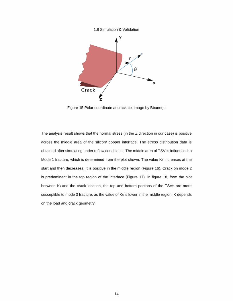
Figure 15 Polar coordinate at crack tip, image by Bbanerje ............................................. 14
Figure 16 . Silicon dies/Cu stress distribution with K1 plot. .............................................. 15
Figure 17 K2 Crack location plot. ...................................................................................... 15
Figure 18 K3 Crack location plot ....................................................................................... 16
Figure 19 Interfacial crack on TSV surface ....................................................................... 16
Figure 20 Max von mises stress test on TSV copper core and SiO2 surface .................. 17
Figure 21 Max stress variation with substrate thickness .................................................. 18
Figure 22 J-integral Vs Substrate thickness for horizontal Crack ..................................... 18
Figure 23 . J Integral Vs Substrate thickness for vertical crack ........................................ 19
Figure 24 J Integral variation on TSV with substrate thickness ........................................ 20
Figure 25 modeled nine crcak on TSV surface at different location ................................. 20
Figure 26 J Integral vs substrate thickness along TSV core for top die thickness 0.1mm
under thermal cycling ........................................................................................................ 21
ix
Figure 27 . J-integral vs substrate thickness along TSV core for top Die thickness 0.4mm
under thermal cycling ........................................................................................................ 22
Figure 28 J-integral vs crack perimeter ............................................................................. 23
Figure 29 Max Equivalent stress vs crack perimeter (mm) ............................................... 23
Figure 30 Different thermal cycle profile ........................................................................... 24
Figure 31 J-integral variation with increasing thermal load............................................... 25
Figure 32 Typical BEOL structure ..................................................................................... 26
Figure 33 SEM cross section of the TSV in a 32nm high-k metal gate technology with
embedded DRAM .............................................................................................................. 26
Figure 34 Sub-modeling technique & Cut boundary condition ......................................... 27
Figure 35 BEOL stack-up .................................................................................................. 28
Figure 36 . Modeling crack at center of dielectric layer .................................................... 28
Figure 37 Equivalent stress distribution on dielectric layer of BEOL ................................ 29
Figure 38 J-integral for crack at Dielectric layers .............................................................. 30
Figure 39 J-integral vs substrate thickness....................................................................... 30
Figure 40 Five different substrate stack up ....................................................................... 31
Figure 41 Change in plastic work on corner solder bump for all stack up ........................ 31
Figure 42 120ZQZ boards with FR4 and RCC Laminate .................................................. 36
Figure 43 Layout and design for 120 pin BGA ................................................................. 37
Figure 44 Picture showing package components (a) Schematic drawing, (b) optical
microscopy image ............................................................................................................. 38
Figure 45 BGA Assembly model with labeled component names .................................... 38
Figure 46 Layer Stack-ups of 1 mm BGA Board .............................................................. 39
Figure 47 Solder Joint Failure occurred on the PCB side ................................................. 40
Figure 48 Failure Occurred on the Substrate Side of the Package .................................. 40
Figure 49 TMA and DMA sample ...................................................................................... 41
Figure 50 Thermomechanical analyzer (TMA), ................................................................ 42
Figure 51 Universal Testing Machine (UTM) .................................................................... 42
Figure 52 Out of plane CTE measurement for both type of BGA. .................................... 43
Figure 53 In-plane CTE measurement for both type of BGA ............................................ 43

x
Figure 54 Dynamic Mechanical Analyzer .......................................................................... 45
Figure 55 DMA 3 point bending attachment ..................................................................... 45
Figure 56 Temperature dependent Elastic modulus results from DMA ............................ 46
Figure 57 DMA result output showing temperature-dependent modulus variation for
different frequency ............................................................................................................ 47
Figure 58 A master curve obtained from TA7000 software .............................................. 47
Figure 59 Non-linear fit using Origin Pro (Time vs magnitude of complex modulus) ....... 48
Figure 60 Sub-modeling concept in a pulley hub .............................................................. 51
Figure 61 BGA Global and Sub model .............................................................................. 51
Figure 62 BGA model mesh sensitive analysis plot .......................................................... 52
Figure 63 Cut boundary condition from global model ....................................................... 53
Figure 64 : Thermal Cycling profile ................................................................................... 54
Figure 65 BGA Layered model ......................................................................................... 54
Figure 66 Equivalent stress on corner solder joint ............................................................ 55
Figure 67 von-Mises equivalent stress for RCC & FR4 prepreg in lumped and layered
model................................................................................................................................. 55
Figure 68 Max Equivalent Elastic Strain Comparison ....................................................... 56
Figure 69 Directional deformation in z direction ............................................................... 56
Figure 70 Maximum directional deformation in all axis ..................................................... 57
Figure 71 Non-linear plastic work distribution on Top portion of corner solder ball .......... 57
Figure 72 Non-linear plastic work distribution on Bottom portion of corner solder ball .... 58
Figure 73 Change in plastic work (ΔW) for both boards ................................................... 59
Figure 74 Power Cycling Profile ........................................................................................ 65
Figure 75 Transient thermal analysis coupled system ...................................................... 66
Figure 76 Power cycling - analysis tress from ANSYS model .......................................... 66
Figure 77 Coupled power and thermal cycling profile ....................................................... 67
Figure 78 Internal heat generation from die ...................................................................... 68
Figure 79 convection on outer surfaces ............................................................................ 69
Figure 80 Temperature distribution due to power cycling ................................................. 69
Figure 81 output max Temperature profile from power cycling ........................................ 70

xi
Figure 82 max temperature for all PCBs ........................................................................... 70
Figure 83 Equivalent stress on all solder balls, corner solder is critical ........................... 71
Figure 84 Critical solder top showing high stress contour ................................................ 71
Figure 85 Max von-Mises stress for different PCB under PC & ATC ............................... 72
Figure 86 Change in plastic work under ATC ................................................................... 73
Figure 87 Change in plastic work under PC ..................................................................... 73
xii
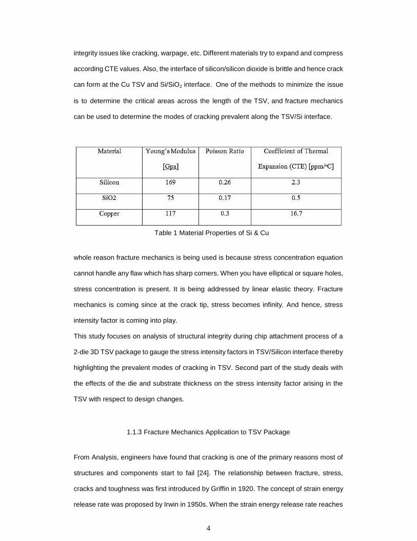
List of Tables Table 1 Material Properties of Si & Cu ................................................................................ 4
Table 2 Anand’s Constants for SAC305 ............................................................................. 8
Table 3 Anand’s Constant for Effective Block in the Compact Model ................................ 9
Table 4 BGA Package material properties........................................................................ 44
Table 5 BGA PCB board material properties .................................................................... 45
Table 6 Anand’s material Constants for SAC 305 ............................................................ 49
Table 7 five PCBs material properties .............................................................................. 67

1
Chapter 1: STRUCTURAL OPTIMIZATION OF 3D TSV PACKAGE
1.1 Introduction
To begin with basic definition, Electronic packaging is a science and art of
providing a suitable environment to the electronic product to perform reliably, over a period.
When we use the word suitable environment, it includes thermal, electrical and other green
issues. It encompasses every technology associated between IC and the system [15]. The
role of electronic packaging is crucial since the performance of the IC’s and the system can
be properly gauged only after the electronic product has been packaged. The various levels
of electronic packaging are broadly classified into:
1. Chip-Level. 2. Board-Level. 3. System-Level.
Chip-Level Packaging: The lowest level of packaging Is the chip level. It consists of steps
and processes in which a bare die is conveniently handled and packaged to use on boards,
etc., since we cannot directly incorporate bare dies to use, though now it has become
possible as well.
On the demand for greater portability of electronic devices, the electronics in today’s
digitized industry are undergoing integration and miniaturization to become smaller and
lighter for ease of its application. The electronic packaging industry is driven by the chips
with more I/O’s and the state of the art multi-functionality. On the other hand, the efficiency
and quality with the reduced cost and power loss must be established, which inspires
manufacturer to do 3D stacking of chips. This necessitates an effective communication
between the IC and the electronic system. Thus, due to low cost, small form factor and
high-performance 3-dimensional integration have emerged as a boost to electronic
2
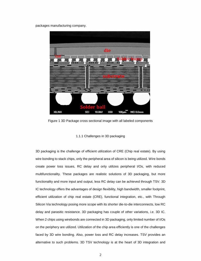
packages manufacturing company.
Figure 1 3D Package cross sectional image with all labeled components
1.1.1 Challenges in 3D packaging
3D packaging is the challenge of efficient utilization of CRE (Chip real estate). By using
wire bonding to stack chips, only the peripheral area of silicon is being utilized. Wire bonds
create power loss issues, RC delay and only utilizes peripheral I/Os, with reduced
multifunctionality. These packages are realistic solutions of 3D packaging, but more
functionality and more input and output, less RC delay can be achieved through TSV. 3D
IC technology offers the advantages of design flexibility, high bandwidth, smaller footprint,
efficient utilization of chip real estate (CRE), functional integration, etc., with Through
Silicon Via technology posing more scope with its shorter die-to-die interconnects, low RC
delay and parasitic resistance. 3D packaging has couple of other variations, i.e. 3D IC.
When 2 chips using wirebonds are connected in 3D packaging, only limited number of I/Os
on the periphery are utilized. Utilization of the chip area efficiently is one of the challenges
faced by 3D wire bonding. Also, power loss and RC delay increases. TSV provides an
alternative to such problems. 3D TSV technology is at the heart of 3D integration and
3
stacking of dies. In a typical TSV package, a thin silicon wafer is drilled with through holes,
and dielectric SiO2 is deposited along the inside walls of t h e holes, and then the hole is
filled with Copper. When the length of the interconnect is less, the resistance and power
loss is less with faster signal processing time. Also, there are more input and output ports
in TSV which lead to improved functionality. Hence we incorporate TSV’s to make 1000’s
of i/p and o/p in a very small area. TSV technology is the future which drives 3D packaging.
However, there are some ongoing issues related to heat removal, structural integrity, chip
package interaction in TSV, which are under research and development.
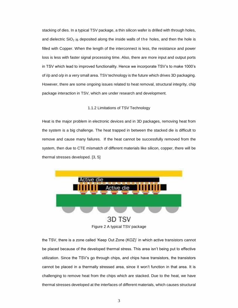
1.1.2 Limitations of TSV Technology
Heat is the major problem in electronic devices and in 3D packages, removing heat from
the system is a big challenge. The heat trapped in between the stacked die is difficult to
remove and cause many failures. If the heat cannot be successfully removed from the
system, then due to CTE mismatch of different materials like silicon, copper, there will be
thermal stresses developed. [3, 5]
the TSV, there is a zone called ‘Keep Out Zone (KOZ)’ in which active transistors cannot
be placed because of the developed thermal stress. This area isn’t being put to effective
utilization. Since the TSV’s go through chips, and chips have transistors, the transistors
cannot be placed in a thermally stressed area, since it won’t function in that area. It is
challenging to remove heat from the chips which are stacked. Due to the heat, we have
thermal stresses developed at the interfaces of different materials, which causes structural
Figure 2 A typical TSV package
4
integrity issues like cracking, warpage, etc. Different materials try to expand and compress
according CTE values. Also, the interface of silicon/silicon dioxide is brittle and hence crack
can form at the Cu TSV and Si/SiO2 interface. One of the methods to minimize the issue
is to determine the critical areas across the length of the TSV, and fracture mechanics
can be used to determine the modes of cracking prevalent along the TSV/Si interface.
whole reason fracture mechanics is being used is because stress concentration equation
cannot handle any flaw which has sharp corners. When you have elliptical or square holes,
stress concentration is present. It is being addressed by linear elastic theory. Fracture
mechanics is coming since at the crack tip, stress becomes infinity. And hence, stress
intensity factor is coming into play.
This study focuses on analysis of structural integrity during chip attachment process of a
2-die 3D TSV package to gauge the stress intensity factors in TSV/Silicon interface thereby
highlighting the prevalent modes of cracking in TSV. Second part of the study deals with
the effects of the die and substrate thickness on the stress intensity factor arising in the
TSV with respect to design changes.
1.1.3 Fracture Mechanics Application to TSV Package
From Analysis, engineers have found that cracking is one of the primary reasons most of
structures and components start to fail [24]. The relationship between fracture, stress,
cracks and toughness was first introduced by Griffin in 1920. The concept of strain energy
release rate was proposed by Irwin in 1950s. When the strain energy release rate reaches
Table 1 Material Properties of Si & Cu
5
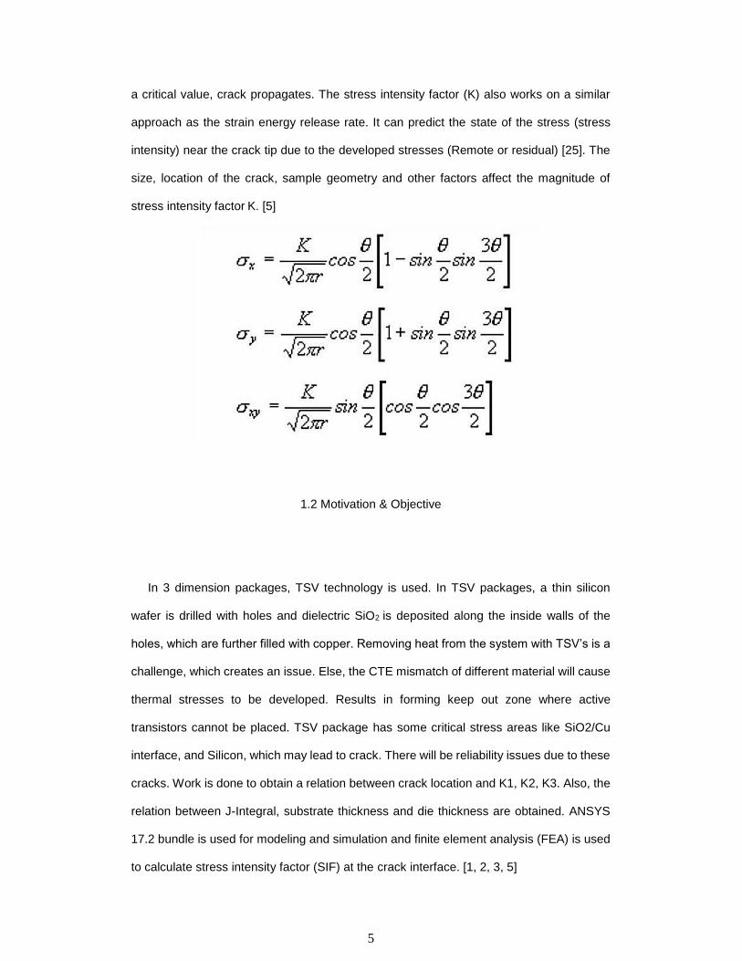
a critical value, crack propagates. The stress intensity factor (K) also works on a similar
approach as the strain energy release rate. It can predict the state of the stress (stress
intensity) near the crack tip due to the developed stresses (Remote or residual) [25]. The
size, location of the crack, sample geometry and other factors affect the magnitude of
stress intensity factor K. [5]
1.2 Motivation & Objective
In 3 dimension packages, TSV technology is used. In TSV packages, a thin silicon
wafer is drilled with holes and dielectric SiO2 is deposited along the inside walls of the
holes, which are further filled with copper. Removing heat from the system with TSV’s is a
challenge, which creates an issue. Else, the CTE mismatch of different material will cause
thermal stresses to be developed. Results in forming keep out zone where active
transistors cannot be placed. TSV package has some critical stress areas like SiO2/Cu
interface, and Silicon, which may lead to crack. There will be reliability issues due to these
cracks. Work is done to obtain a relation between crack location and K1, K2, K3. Also, the
relation between J-Integral, substrate thickness and die thickness are obtained. ANSYS
17.2 bundle is used for modeling and simulation and finite element analysis (FEA) is used
to calculate stress intensity factor (SIF) at the crack interface. [1, 2, 3, 5]
6
1.3 Outline
ANSYS 17.2 is being leveraged for modeling all types of cracks. Quarter symmetry TSV
package is modeled in same software, which was used to simulate the reflow condition
and thermal cycling to analyze the various stresses developed within the TSV package.
The temperature boundary condition subjected to the package was 200°C. The sub-
modeling technique was used to analyze the copper core of the TSV. The cracks are
modeled at a different position on TSV and different dielectric layers of BEOL to study
crack behavior. Die and substrate thickness was varied to study the behavior of stress
intensity factor and J-integral. Nine cracks were modeled along the TSV with the same
direction. Two independent loading conditions were tested and J-integral variation was
studied by varying the substrate and die thickness. Two independent loading conditions
are Reflow condition and Thermal cycling.
1.4 Model Description
2 die 3-D flip chip package along with the TSV has been studied with respect to the
crack propagation analysis. The response of this package after connecting substrate and
the chip has also been studied. TSV has a diameter of 10μm including 0.5μm of the area
covered by a dielectric. To avoid the adverse effects of silicon efficiency, the TSV is
restricted to less than 4 percent. Mirza et al. and Chirag et al. have put forward a novel
approach that demonstrates how reasonably computational time can be maintained. There
are 3 steps that play a vital role in simulation. Initially, a global model on the compact scale
is formulated and solved. The results from this solution are used to generate boundary
conditions to the sub model 1 which is part of the critical region having detailed features
(for example practical μ-bump interconnections and TSVs). [8, 11] These boundary
conditions are applied on the sub model 2 which is part of the sub model 1. To prevent
rigid body motions, a center node at the bottom is fixed and normal displacement with
respect to the symmetric faces are constrained. Using linear elastic material properties
7
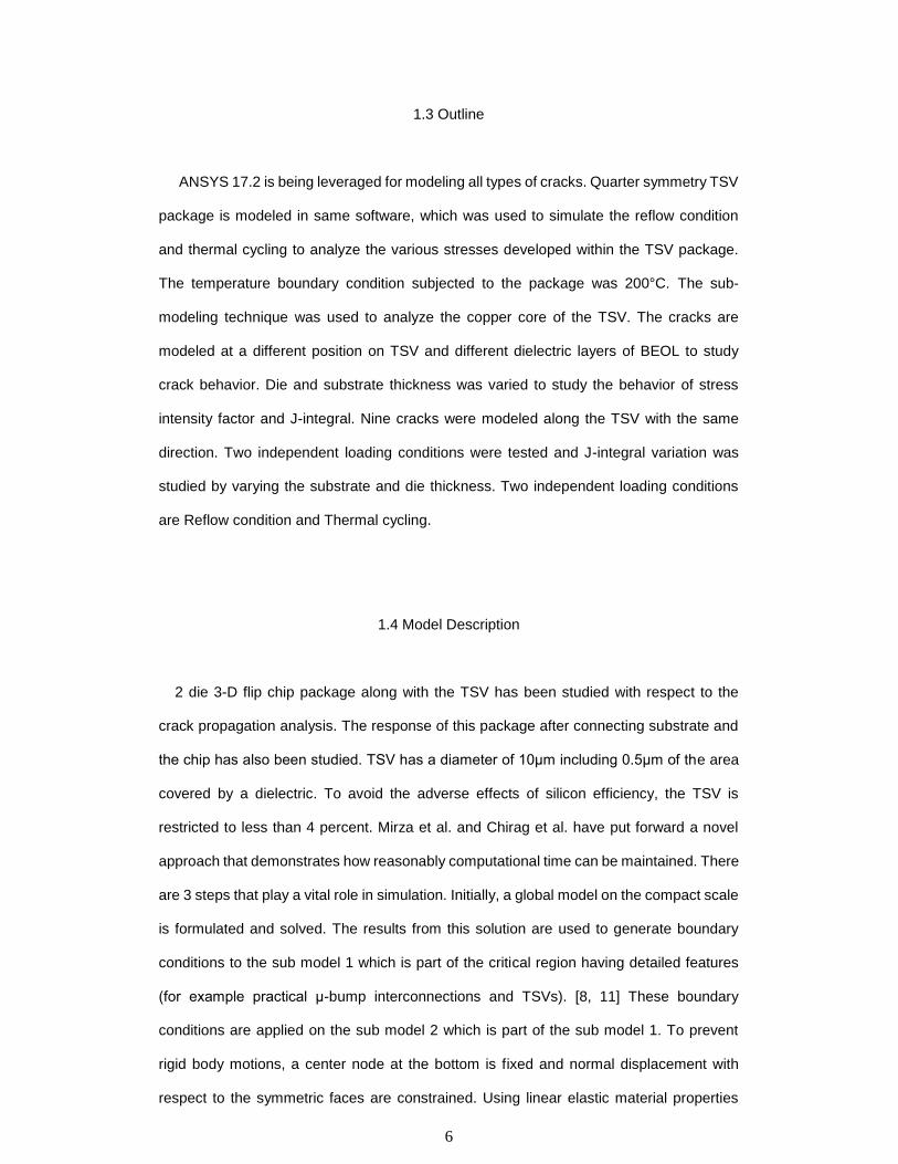
from Rajmane et al, all the materials except copper (TSVs and BEOL) and solder (SAC305)
are modeled. [6] Using Anand’s viscoplastic model and considering the creep and plastic
deformations (representing secondary creep), solder is modeled as rate dependent
viscoplastic material. To describe the inelastic behavior of lead-free solder, Anand’s
viscoplastic constitutive law has been used. Anand’s law has an impact on a total of nine
material constants A, Q, ξ, m, n, h, a, s, ŝ (all of which are extracted from the curve fitting
experimental data) that are used throughout the solder strain-rate and temperature
sensitivity. [5]
Figure 3 Global model with highlighted solder bumps and TSV from sub model 1
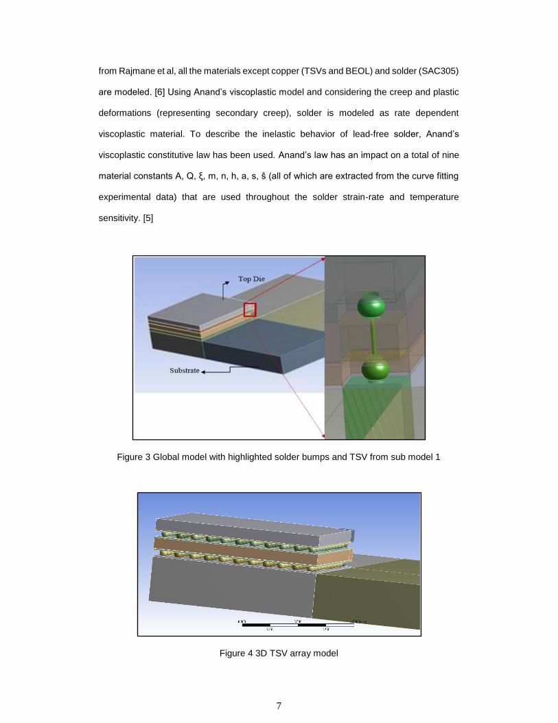
Figure 4 3D TSV array model

8
Figure 5 3D TSV model without die to show solder & TSV array
Figure 6 3S TSV model with effective block
Table 2 Anand’s Constants for SAC305
S. No. Anand’s Constant
Units Value
1 s 0
MPa 1.3
2 Q/R 1/K 9000
3 A Sec-1 500
4 ξ Dimensionless 7.1
5 m Dimensionless 0.3
6 H0 MPa 5900
7 ŝ MPa 39.5
8 n Dimensionless 0.03
9 a Dimensionless 1.5

9
Table 3 Anand’s Constant for Effective Block in the Compact Model
S. No. Anand’s Constant
Units Value
1 S0 MPa 0.15
2 Q/R 1/K 9000
3 A Sec-1 500
4 ξ Dimensionless 7.1
5 M Dimensionless 0.3
6 h0 MPa 5900
7 Ŝ MPa 3
8 N Dimensionless 0.03
9 A Dimensionless 1.5
1.5 Loads and Boundary Conditions
Figure 7 Symmetry region and supports
Figure 8 uniformly distributed thermal load throughout the body

10
Figure 9 reflow condition thermal load profile
1.5.1 Assumptions • Each layer in the package is perfectly bonded to other.
• All materials except solder alloy (SAC305) are modeled using linear elastic
material properties.
• Time and temperature dependent material properties were used from
Anand’s Viscoplastic Model to capture the inelastic behavior of SAC305.
• All components considered stress free at 200°C (reflow temperature).
1.5.2 Boundary Conditions • Symmetry boundary conditions were taken at the Quarter symmetry faces.
• Common vertex of the PCB was fixed (All DOF zero) to restrict any rigid body
motion.
• Reflow process for chip attachment to the substrate has been simulated –
200°C to Room at 30°C /min.
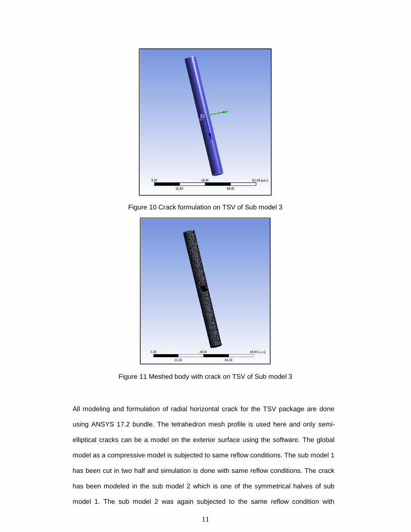
1.6 Crack Modeling Crack propagation is placed in a different location along the cylindrical silicon die interposer
where the TSV and copper passes. In this experiment, silicon and silicon dioxide are
covered as the critical area on TSV interface. Therefore, the crack is modeled successfully
along the silicon die/Cu interface. This is the prominent region for critical stresses acting
where more chances of crack to be developed.
11
Figure 10 Crack formulation on TSV of Sub model 3
Figure 11 Meshed body with crack on TSV of Sub model 3
All modeling and formulation of radial horizontal crack for the TSV package are done
using ANSYS 17.2 bundle. The tetrahedron mesh profile is used here and only semi-
elliptical cracks can be a model on the exterior surface using the software. The global
model as a compressive model is subjected to same reflow conditions. The sub model 1
has been cut in two half and simulation is done with same reflow conditions. The crack
has been modeled in the sub model 2 which is one of the symmetrical halves of sub
model 1. The sub model 2 was again subjected to the same reflow condition with
12
importing cut boundary constraints from the sub model 1.10 divisions with equal space
have been taken for simulation of the crack where the total edge length of TSV is 95 μm.
All the simulations are done along the length of TSV in sub model 2 with an equal division
of 9.5 μm. When it is attached to the substrate, reflow condition is taken for thermal
loading in 3D TSV package from 200oC to room temperature (for Pb-free SAC305 Alloy).
The plot for the relation between stress intensity factor (SIF) (i.e. K1, K2, K3) and crack
location have been shown in this study. Also, the relation between crack size, crack length
and J-integral is shown in the plot. The results show that the TSV area is much affected
by mode 1, mode 2 and mode 3 cracking. To avoid radial crack, K should be less than
Kc, i.e. K<Kc where Kc is fracture toughness of silicon.
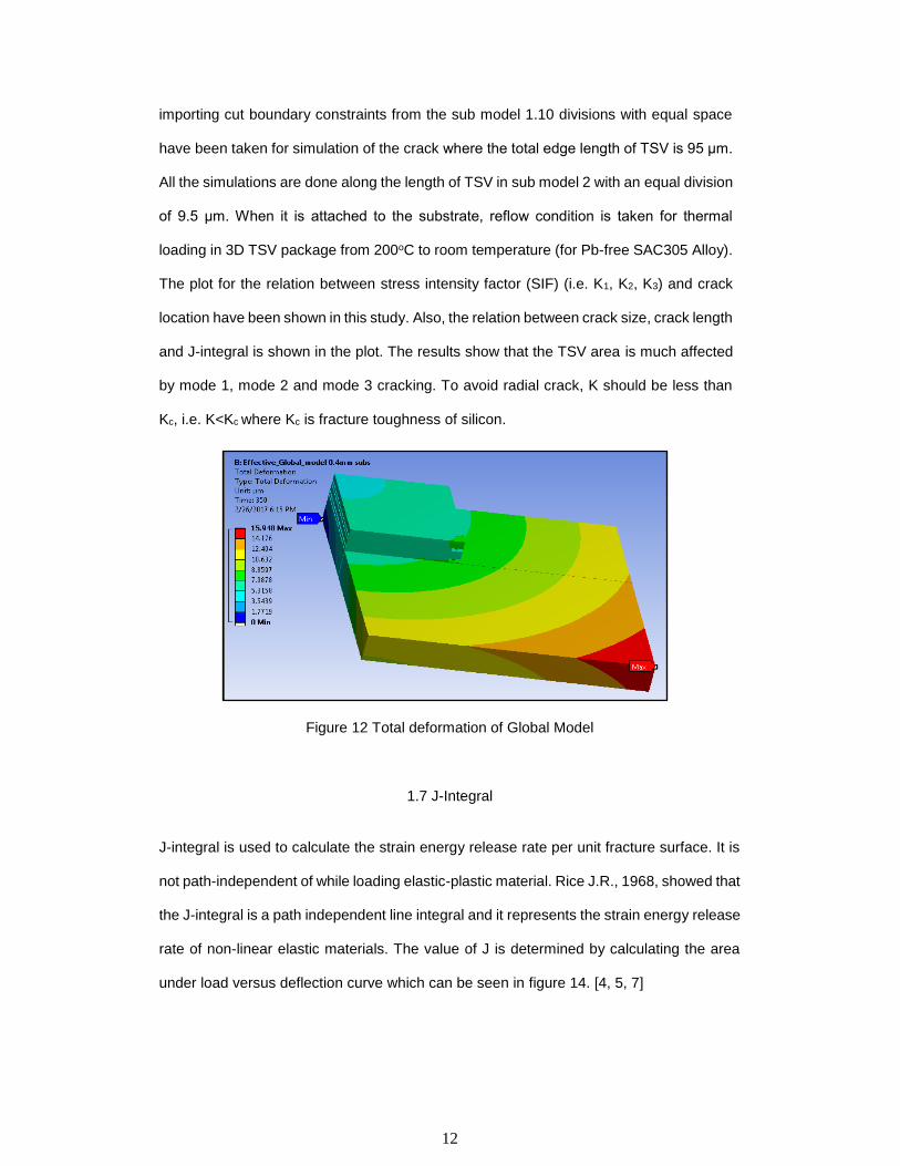
Figure 12 Total deformation of Global Model
1.7 J-Integral
J-integral is used to calculate the strain energy release rate per unit fracture surface. It is
not path-independent of while loading elastic-plastic material. Rice J.R., 1968, showed that
the J-integral is a path independent line integral and it represents the strain energy release
rate of non-linear elastic materials. The value of J is determined by calculating the area
under load versus deflection curve which can be seen in figure 14. [4, 5, 7]

13
Figure 13 line integral around crack tip
Figure 14 J integral explanation (Load vs Deflection plot)
Where W is the strain energy density per unit volume, ds is an infinitesimal element of the
contour are length, Γ denotes any contour path surrounding the crack tip, and T and u are
traction and displacement vectors along Γ Curve.
14
1.8 Simulation & Validation
Figure 15 Polar coordinate at crack tip, image by Bbanerje
The analysis result shows that the normal stress (in the Z direction in our case) is positive
across the middle area of the silicon/ copper interface. The stress distribution data is
obtained after simulating under reflow conditions. The middle area of TSV is influenced to
Mode 1 fracture, which is determined from the plot shown. The value K1 increases at the
start and then decreases. It is positive in the middle region (Figure 16). Crack on mode 2
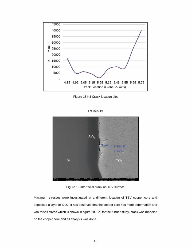
is predominant in the top region of the interface (Figure 17). In figure 18, from the plot
between K3 and the crack location, the top and bottom portions of the TSVs are more
susceptible to mode 3 fracture, as the value of K3 is lower in the middle region. K depends
on the load and crack geometry

15
Figure 16 . Silicon dies/Cu stress distribution with K1 plot
Figure 17 K2 Crack location plot.
-45000
-40000
-35000
-30000
-25000
-20000
-15000
-10000
-5000
0
5000
10000
4.85 4.95 5.05 5.15 5.25 5.35 5.45 5.55 5.65 5.75
K1
P
a.m
1/2
Crack Location (Global Z- Axis)
-10000
0
10000
20000
30000
40000
50000
60000
4.85 4.95 5.05 5.15 5.25 5.35 5.45 5.55 5.65 5.75
K2
P
a.m
1/2
Crack Location (Global Z- Axis)
16
Figure 18 K3 Crack location plot
1.9 Results
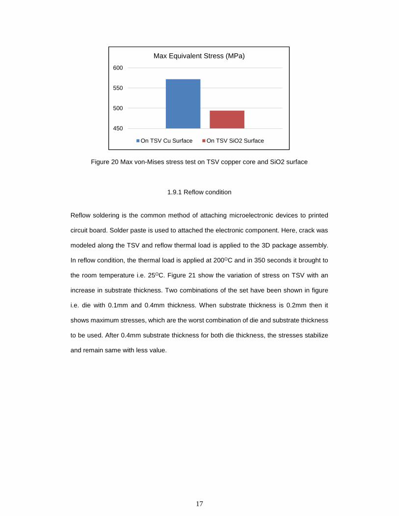
Figure 19 Interfacial crack on TSV surface
Maximum stresses were investigated at a different location of TSV copper core and
deposited a layer of SiO2. It has observed that the copper core has more deformation and
von-mises stress which is shown in figure 20. So, for the further study, crack was modeled
on the copper core and all analysis was done.
0
5000
10000
15000
20000
25000
30000
35000
40000
45000
4.85 4.95 5.05 5.15 5.25 5.35 5.45 5.55 5.65 5.75
K3
P
a.m
1/2
Crack Location (Global Z- Axis)
17
Figure 20 Max von-Mises stress test on TSV copper core and SiO2 surface
1.9.1 Reflow condition
Reflow soldering is the common method of attaching microelectronic devices to printed
circuit board. Solder paste is used to attached the electronic component. Here, crack was
modeled along the TSV and reflow thermal load is applied to the 3D package assembly.
In reflow condition, the thermal load is applied at 200OC and in 350 seconds it brought to
the room temperature i.e. 25OC. Figure 21 show the variation of stress on TSV with an
increase in substrate thickness. Two combinations of the set have been shown in figure
i.e. die with 0.1mm and 0.4mm thickness. When substrate thickness is 0.2mm then it
shows maximum stresses, which are the worst combination of die and substrate thickness
to be used. After 0.4mm substrate thickness for both die thickness, the stresses stabilize
and remain same with less value.
450
500
550
600
Max Equivalent Stress (MPa)
On TSV Cu Surface On TSV SiO2 Surface
18
Figure 21 Max stress variation with substrate thickness
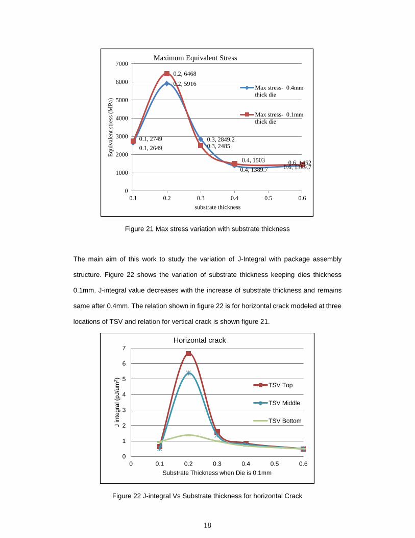
The main aim of this work to study the variation of J-Integral with package assembly
structure. Figure 22 shows the variation of substrate thickness keeping dies thickness
0.1mm. J-integral value decreases with the increase of substrate thickness and remains
same after 0.4mm. The relation shown in figure 22 is for horizontal crack modeled at three
locations of TSV and relation for vertical crack is shown figure 21.
Figure 22 J-integral Vs Substrate thickness for horizontal Crack
0.1, 2649
0.2, 5916
0.3, 2849.2
0.4, 1389.7 0.6, 1389.7
0.1, 2749
0.2, 6468
0.3, 2485
0.4, 1503 0.6, 1452
0
1000
2000
3000
4000
5000
6000
7000
0.1 0.2 0.3 0.4 0.5 0.6
Eq
uiv
alen
t st
ress
(M
Pa)
substrate thickness
Maximum Equivalent Stress
Max stress- 0.4mm
thick die
Max stress- 0.1mm
thick die
0
1
2
3
4
5
6
7
0 0.1 0.2 0.3 0.4 0.5 0.6
J in
teg
ral (p
J/u
m2)
Substrate Thickness when Die is 0.1mm
Horizontal crack
TSV Top
TSV Middle
TSV Bottom

19
Figure 23 . J Integral Vs Substrate thickness for vertical crack
1.9.2 Thermal Cycling:
Thermal cycling is a most common method to check strength electronic device assembly
against the thermal load. It is conducted to determine the ability of components and solder
joints and interconnects. The method of thermal cycling was referred from JEDEC standard
JESD22-A104D. Experimentally this test is done in an environmental chamber with the
same condition mentioned in standards. Devolved mechanical stresses can be used to
investigate the solder joint or assembly reliability. The temperature varies from -40OC to
125OC for 10800 sec. the dwell and ramp time is 15mins. A total of three cycles was applied
to the package. Like reflow condition, crack was modeled on the TSV core at different
location and variation of J-integral was studied with respect to substrate thickness and with
changing top die thickness. Figure 24 shows the variation of J-integral value for the
different size of the substrate for two different top die size. In this study, two cracks were
modeled at the top and bottom of TSV. When the thickness of top die is 0.1mm the variation
of j integral value was noted. The J-integral value decreases with increase in substrate
thickness and then increase to some extend and stabilize after 0.4mm thickness. Similarly,
0
1
2
3
4
5
6
0 0.1 0.2 0.3 0.4 0.5 0.6
J inte
gra
l (p
J/u
m2)
subs thikness [die - 0.1mm]
vertical crack
TSV Top
TSV Middle
TSV Bottom
20
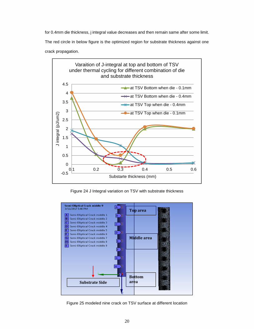
for 0.4mm die thickness, j integral value decreases and then remain same after some limit.
The red circle in below figure is the optimized region for substrate thickness against one
crack propagation.
Figure 24 J Integral variation on TSV with substrate thickness
Figure 25 modeled nine crack on TSV surface at different location
-0.5
0
0.5
1
1.5
2
2.5
3
3.5
4
4.5
0.1 0.2 0.3 0.4 0.5 0.6
J inte
gra
l (p
J/u
m2)
Substarte thickness (mm)
Varaition of J-integral at top and bottom of TSV under thermal cycling for different combination of die
and substrate thickness
at TSV Bottom when die - 0.1mm
at TSV Bottom when die - 0.4mm
at TSV Top when die - 0.4mm
at TSV Top when die - 0.1mm
Top area
Middle area
Bottom area Substrate Side
21
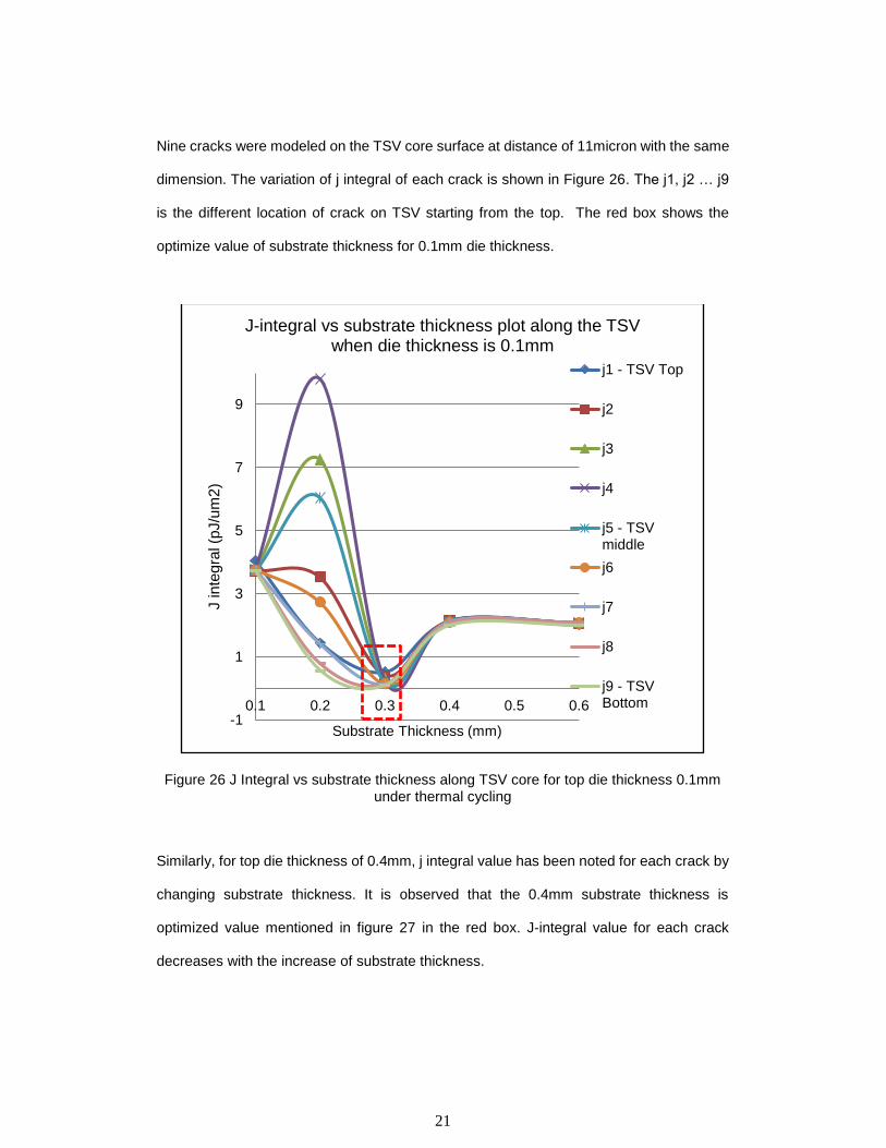
Nine cracks were modeled on the TSV core surface at distance of 11micron with the same
dimension. The variation of j integral of each crack is shown in Figure 26. The j1, j2 … j9
is the different location of crack on TSV starting from the top. The red box shows the
optimize value of substrate thickness for 0.1mm die thickness.
Figure 26 J Integral vs substrate thickness along TSV core for top die thickness 0.1mm under thermal cycling
Similarly, for top die thickness of 0.4mm, j integral value has been noted for each crack by
changing substrate thickness. It is observed that the 0.4mm substrate thickness is
optimized value mentioned in figure 27 in the red box. J-integral value for each crack
decreases with the increase of substrate thickness.
-1
1
3
5
7
9
0.1 0.2 0.3 0.4 0.5 0.6
J in
teg
ral (p
J/u
m2
)
Substrate Thickness (mm)
J-integral vs substrate thickness plot along the TSV when die thickness is 0.1mm
j1 - TSV Top
j2
j3
j4
j5 - TSVmiddle
j6
j7
j8
j9 - TSVBottom

22
Figure 27 . J-integral vs substrate thickness along TSV core for top Die thickness 0.4mm under thermal cycling
J-integral value is line integral of the crack tip. So, per literature survey, the value of J-
integral should increase with an increase in crack size. For a detailed analysis of the study
on 3D TSV package, crack size was increased and the j integral value has been noted.
Figure 28 shows the relation of crack perimeter and j integral value.
0
0.2
0.4
0.6
0.8
1
1.2
1.4
1.6
1.8
2
0.1 0.2 0.3 0.4 0.5 0.6
J inte
gra
l (p
J/u
m2)
Substrate Thickness (mm)
J-integral vs substrate thickness plot along the TSV when die thickness is 0.4mm
j1 - TSV Top
j2
j3
j4
j5 - TSV middle
j6
j7
j8
j9 - TSV Bottom

23
Figure 28 J-integral vs crack perimeter
Also, the variation of maximum equivalent elastic strain value has been noted for different
crack size. The relation between strain and the crack perimeter is shown in figure 29. The
maximum strain value increases first and then decreases up to a certain limit. After 7-
micron crack perimeter, the strain stabilizes and remain same with an increase in crack
size.
Figure 29 Max Equivalent stress vs crack perimeter (mm)
0.1
0.15
0.2
0.25
0.3
0.35
2.00E-06 6.00E-06 1.00E-05 1.40E-05
J inte
gra
l (p
J/u
m2)
Crack Perimeter
0
0.02
0.04
0.06
0.08
0.1
0.12
0.14
1.00E-06 4.00E-06 7.00E-06 1.00E-05 1.30E-05
Max E
quiv
ale
nt
Str
ain
Crack Perimeter (m)
24
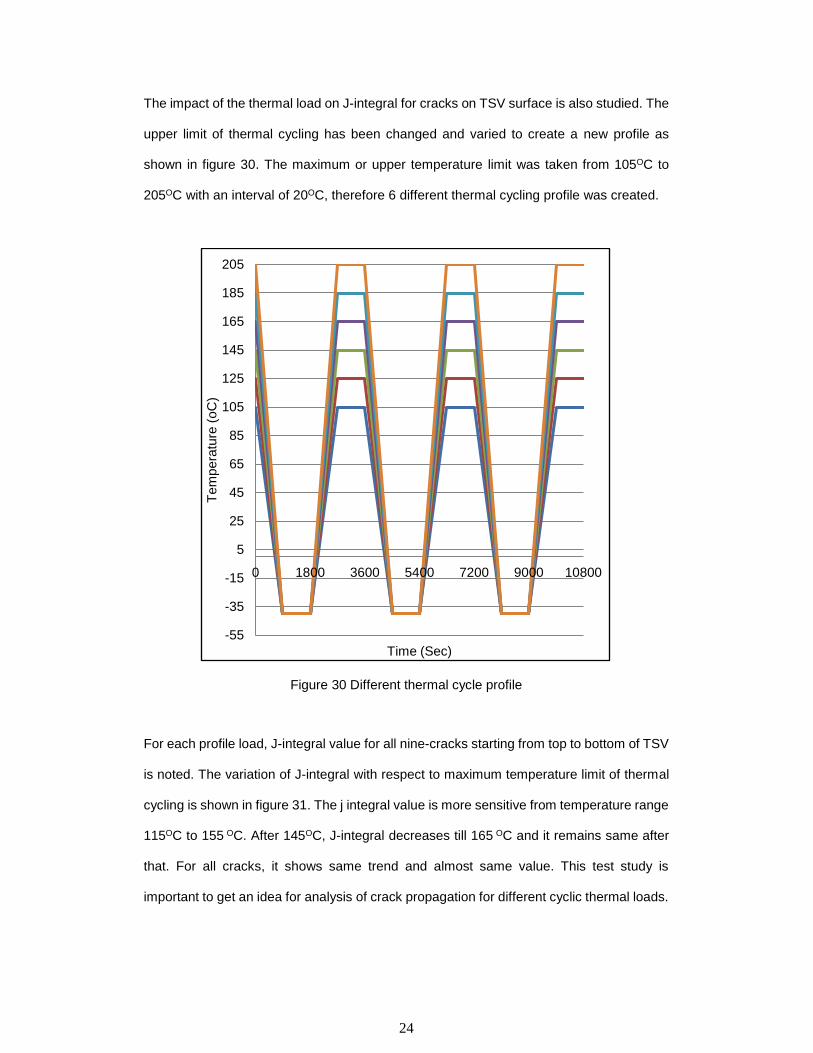
The impact of the thermal load on J-integral for cracks on TSV surface is also studied. The
upper limit of thermal cycling has been changed and varied to create a new profile as
shown in figure 30. The maximum or upper temperature limit was taken from 105OC to
205OC with an interval of 20OC, therefore 6 different thermal cycling profile was created.
Figure 30 Different thermal cycle profile
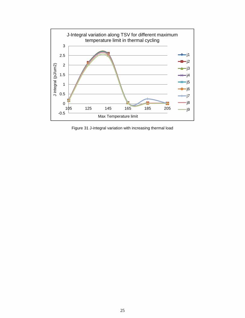
For each profile load, J-integral value for all nine-cracks starting from top to bottom of TSV
is noted. The variation of J-integral with respect to maximum temperature limit of thermal
cycling is shown in figure 31. The j integral value is more sensitive from temperature range
115OC to 155 OC. After 145OC, J-integral decreases till 165 OC and it remains same after
that. For all cracks, it shows same trend and almost same value. This test study is
important to get an idea for analysis of crack propagation for different cyclic thermal loads.
-55
-35
-15
5
25
45
65
85
105
125
145
165
185
205
0 1800 3600 5400 7200 9000 10800
Tem
pera
ture
(oC
)
Time (Sec)
25
Figure 31 J-integral variation with increasing thermal load
-0.5
0
0.5
1
1.5
2
2.5
3
105 125 145 165 185 205
J inte
gra
l (p
J/u
m2)
Max Temperature limit
J-Integral variation along TSV for different maximum temperature limit in thermal cycling
j1
j2
j3
j4
j5
j6
j7
j8
j9

26
1.10 J-Integral Variation Due to Semielliptical Crack at BEOL
Figure 32 Typical BEOL structure
Figure 33 SEM cross section of the TSV in a 32nm high-k metal gate technology with embedded DRAM
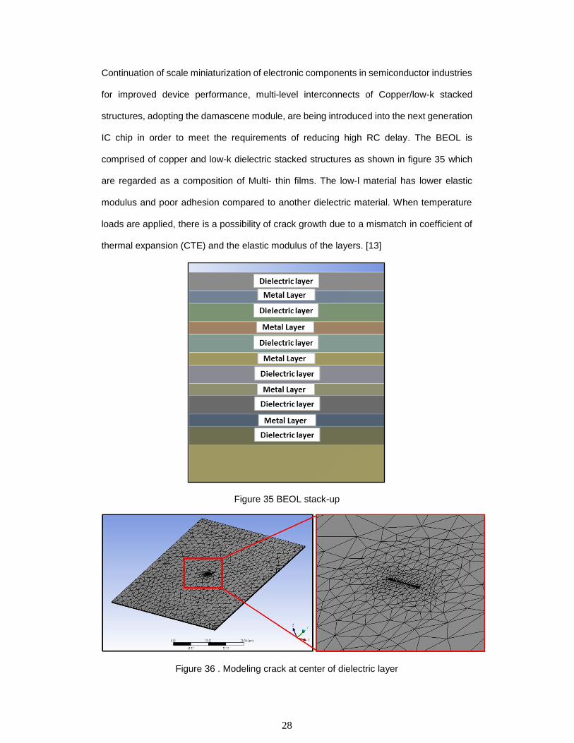
BEOL reliability is challenging part in today’s microelectronic manufacturing industries. The
bonding process of IC undergoes a large plastic deformation which requires a special
attention from the modeling point of view. The low-k material in BEOL are the mechanically
weak but are important for reducing the electrical losses. In place of gold wire bonding,
copper wire bondings are used. As copper has a higher yield stress than gold [12], higher
27
forces act on a mechanical weak structure. The thermomechanical reliability of BEOL is as
important as solder bumps, TSVs, and other components. The stability of the J-integral
value obtained from the FEA is important to avoid a misunderstanding of the cracking
energy. To study the impact of thermal load on crack at different layers of dielectric, BEOL
stack up is incorporated. In sub-model shown in figure 33, 11 layers consisting of 5 metal
layer and 6 dielectric layers alternatively stacked on each other. Each layer is 1.4micron in
thickness. Similarly, to TSV, the same type of study has been done here. Leveraging finite
element modeling, we have modeled semi-elliptical crack on a different dielectric layer of
BEOL. The study will show the variation of J-integral of crack from top dielectric layer to
bottom layer. The sub-modeling technique is used for analysis and fracture tool for
modeling crack. Figure 34 shows all sub-models used and the cut boundary condition
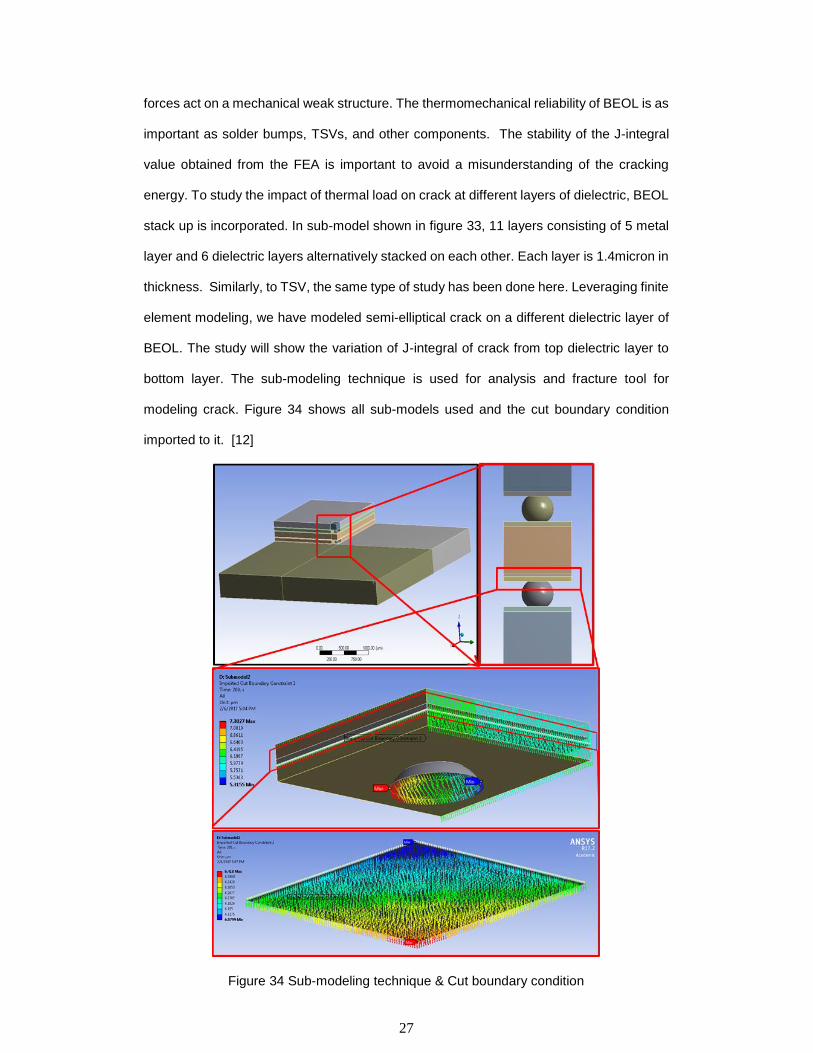
imported to it. [12]
Figure 34 Sub-modeling technique & Cut boundary condition
28
Continuation of scale miniaturization of electronic components in semiconductor industries
for improved device performance, multi-level interconnects of Copper/low-k stacked
structures, adopting the damascene module, are being introduced into the next generation
IC chip in order to meet the requirements of reducing high RC delay. The BEOL is
comprised of copper and low-k dielectric stacked structures as shown in figure 35 which
are regarded as a composition of Multi- thin films. The low-l material has lower elastic
modulus and poor adhesion compared to another dielectric material. When temperature
loads are applied, there is a possibility of crack growth due to a mismatch in coefficient of
thermal expansion (CTE) and the elastic modulus of the layers. [13]
Figure 35 BEOL stack-up
Figure 36 . Modeling crack at center of dielectric layer
29
Figure 36 shows the mesh modeling of the crack size on the top dielectric layer of BEOL.
Similar crack location and size are done for other layers too. A semi-elliptical crack with
0.5micron major axis and 0.1micron minor axis was modeled.
Further, the thermal load applied to the model is reflow condition starting from 200OC to
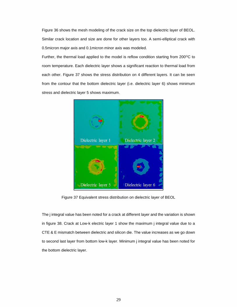
room temperature. Each dielectric layer shows a significant reaction to thermal load from
each other. Figure 37 shows the stress distribution on 4 different layers. It can be seen
from the contour that the bottom dielectric layer (i.e. dielectric layer 6) shows minimum
stress and dielectric layer 5 shows maximum.
Figure 37 Equivalent stress distribution on dielectric layer of BEOL
The j integral value has been noted for a crack at different layer and the variation is shown
in figure 38. Crack at Low-k electric layer 1 show the maximum j integral value due to a
CTE & E mismatch between dielectric and silicon die. The value increases as we go down
to second last layer from bottom low-k layer. Minimum j integral value has been noted for
the bottom dielectric layer.

30
Figure 38 J-integral for crack at Dielectric layers
Figure 39 J-integral vs substrate thickness
Further study includes the substrate thickness optimization and identifying the best
dimension against crack propagation. We increased the substrate thickness from 0.1mm
to 0.6mm by an interval of 0.1mm and noted j integral of crack at top dielectric for each
dimension. The plot between J-integral and substrate thickness is shown in figure 39. The
J-integral value shows maximum for 0.3mm substrate thickness and after 0.4mm substrate
thickness, it gets stabilized. From the analysis, we can conclude that substrate thickness
of 0.4mm is the best fit against crack propagation at BEOL.
0.05
0.06
0.07
0.08
0.09
0.1
0.11
0.12
0.13
1 2 3 4 5 6
J in
teg
ral (p
J/u
m2
)
Dielectric layer No. (From Top)
-0.01
0
0.01
0.02
0.03
0.04
0.05
0.1 0.2 0.3 0.4 0.5 0.6
J in
teg
ral (p
J/u
m2
)
Substrate thickness

31
1.11 3D Package Substrate Stack-Up Study
• Substrate composition plays a vital role in the reliability of any package
• In this study, different stack up was analyzed by changing copper core thickness
by keeping total substrate thickness constant.
• As the core thickness increases, ∆W also increases which is inversely proportional
to life to failure.
• Copper content makes PCB/substrate more rigid.
Figure 40 Five different substrate stack up
Figure 41 Change in plastic work on corner solder bump for all stack up
0
50
100
150
200
250
300
350
400
450
Stack upI
Stack upII
Stack upIII
Stack upIV
Stack upV
Solder mask
Prepreg
Core
Prepreg
Solder mask
0.25
0.3
0.35
0.4
0.45
0.5
0.55
50um 100um 150um 200um 250um
∆ w

32
1.12 Conclusion
The package, PCB, and crack modeling were done successfully. The variation of radial
crack or crack propagation along the TSV Cu core and on low-k dielectric layers of BEOL
has been successfully studied. The cut boundary condition from the global model and sub
model were used for simulation. The variation of J-integral and other parameters were
studied for a different combination of substrate and top die thickness. The J-integral value
is used in calculating strain energy release rate per unit fracture surface area and is
determined with respect to crack size. Six different type of thermal cycle profiles were
created and variation of J-integral value has been studied. The variation of crack size has
also been successfully leveraged to investigate its effect on stress and strain distribution
and found that it was directly proportional to J- integral, whereas the relation between J-
integral and top die-substrate thickness shows an inversely proportional relational property
up to a certain limit of thickness. For 0.1mm die thickness, 0.3mm substrate thickness is
most reliable against crack propagation and for 0.4mm die thickness, 0.4mm substrate
thickness is most reliable. This combination creates a zone of reliable area of substrate
thickness from 0.3mm to 0.4mm. In further, the impact of reflow condition on crack at
different low-k dielectric layer was studied. The relation between a substrate thickness and
j integral of crack at a dielectric layer is obtained. This study is important for optimizing the
package geometry under different loading condition and understanding of crack
propagation depending on structural integrity. Different crack size at a different location
can be studied as per requirement following the same concept.
33
1.13 References
[1] Ramm P, Wolf, MJ, Klumpp A, et al, “Through-silicon via technology – processes and
reliability for wafer-level 3D system integration”, 58th Electronic Components and
Technology Conference, Orlando, FL, pp.841-846,2008.
[2] Khan N, Rao S, Lim S, et al, “Development of 3D silicon module with TSV for the
system in packaging”, 58th Electronic Components and Technology Conference,
Orlando, FL, pp.550-555, 2008.
[3] Lau JH. Overview and outlook of through-silicon via (TSV) and 3D integrations. Micro-
electron Int 2011; 28:8–22.
[4] J. R. Rice, “A path independent integral and the approximate analysis of strain
concentration by notches and cracks”.
[5] Mohammed Shahid Ali, “Estimation of fracture mechanics parameters in 3D TSV
package during chip attachment process”.
[6] Pavan Rajmane, F. Mirza, et al, “Chip Package Interaction to Analyze the Mechanical
Integrity of a 3-D TSV Package”,2015.
[7] N. E. Dowling and J. A. Begley,” Fatigue crack growth during gross plasticity and the J-
integral”.
[8] Fahad Mirza, “Compact Modeling Methodology Development for Thermo-Mechanical
Assessment in High-End Mobile Applications” - Planar 3D TSV Packages, Arlington,
TX,2014.
[9] Karmarkar AP, Xu X, Moroz V. Performance and reliability analysis of 2D integration
structures employing through silicon via (TSV). In: Proc IEEE 47. Annual IntReliab Phys
Symp; 2009. p. 682–7.
[10] Reiske R, Landgraf R and Wolter KJ, “Novel method for crystal defect analysis of
laser drilled TSVs”, 59th Electronic Components and Technology Conference, San Diego,
CA, pp.1139- 1146, 2009.
34
[11] C. Shah, Fahad Mirza, and C. S. Premachandran, "Chip Package Interaction(CPI)
Risk Assessment On 28nm Back End of Line(BEOL) Stack of A Large I/O Chip Using
Compact 3D FEA Modeling," in EPTC, Singapore, 2013.
[12] Dominiek Degryse, Bart Vandevelde, D. Stoukatch, Eric Bcyne, “Mechanical
Behavior of BEOL structures containing Low-k during bonding process” in EPTC 2003
[13] Chang-Chun Lee, Chein-Chia Chiu, Kuo-Ning Chiang, “Stability of j integral
calculation in the crack growth of copper/low-k stacked structures” Thermal and
Thermomechanical Phenomena in Electronics Systems, - ITHERM 2006
35
Chapter 2: RELIABILITY STUDY OF BGA PACKAGE FOR PCB WITH RCC & FR4
PREPREG
2.1 Introduction
BGA is a type of Surface Mount Technology packages. BGA is used extensively due to its
robust design with many interconnects and improved connectivity with lower thermal
resistance. Intensive research and development on BGA motivate us to study in detail
about the layer stack up for the corresponding boards. This variety of material in a single
package results in building into a complex system and increasingly retains elevated levels
of reliability. Reliability is dependent on numerous factors like the operation of the device,
power consumption, heat dissipation and the environment (ambient temperature,
temperature changes, environmental strains).
Types of BGA Packages.
Based on the material used and connectivity and other features, the BGA package is
classifies into 5 types.
MAPBGA – Molded Array Process Ball Grid Array
PBGA – Plastic Ball Grid Array
TEPBGA – Thermally Enhanced Plastic Ball Grid Array
TBGA – Tape Ball Grid Array
Micro BGA
2.2 Motivation & Objective
The buildup layer of PCB affects the reliability of solder joints; it affects the creep strain
range, stress range, creep strain energy density ranges and the thermal fatigue life [9].
The solder balls on a populated PCB absorb all the strains due to the expansion of the
package and by the PCB in thermal excursions. At high temperatures, there is a high

36
possibility of the solder joint to fail due to the CTE mismatch between the PCB and the
package [1]. Also, the stiffness of a PCB is higher than the package which affects the
reliability of a solder joint. [13] In this work, the study of the effect of RCC and FR4 prepreg
layers on solder joint failure for two different PCB is presented. To analyze the failure, we
use ATC as the test. The simulations are run for the temperatures loading from -40⁰C to
125⁰C, and dwell and ramp time of 15mins. The work includes two types of BGA boards,
using RCC and FR4 as the prepregs at the outermost layers. In this work, we have
investigated the board level reliability of these two different boards. Finite Element Analysis
(FEA) is used to determine the fatigue co-relation parameters such as elastic strain,
stresses, directional deformation and accumulated volume average plastic work to predict
the characteristic life of the package.
Figure 42 120ZQZ boards with FR4 and RCC Laminate
37
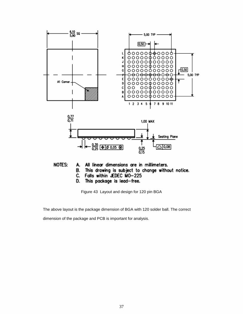
Figure 43 Layout and design for 120 pin BGA
The above layout is the package dimension of BGA with 120 solder ball. The correct
dimension of the package and PCB is important for analysis.

38
Figure 44 Picture showing package components (a) Schematic drawing, (b) optical microscopy image
Figure 44 shows a clear picture of the components of the Ball Grid Package. The package
basically comprises a copper pad on the top and bottom side of the solder bump. On the
die side, the silicon die is attached which is further attached to polyimide layer with an
adhesive layer in the middle. The solder mask in present both, the PCB side and the
substrate side as shown in the schematic.
Figure 45 BGA Assembly model with labeled component names
The dimension from the drawings, X-Ray images, and the cross-section images are
considered in creating a 3D model of the BGA Package. The FE modeled BGA package
is shown in figure 45. Symmetry allows for an octant symmetric model resulting in
39
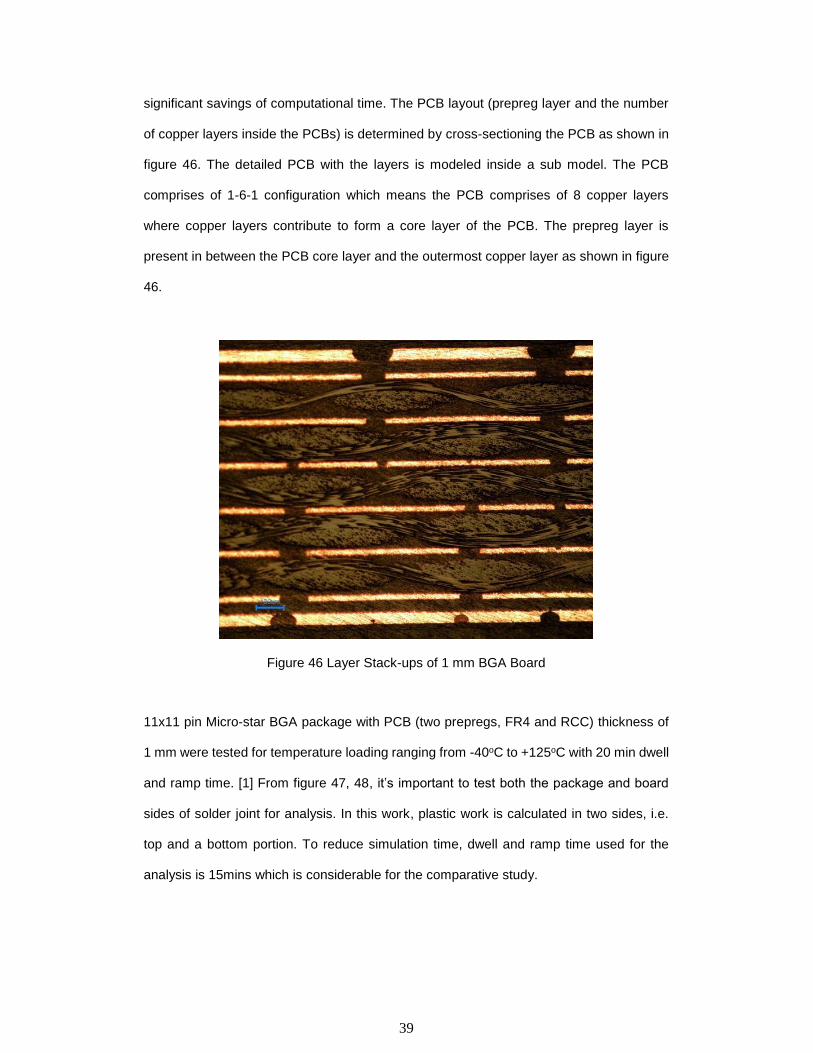
significant savings of computational time. The PCB layout (prepreg layer and the number
of copper layers inside the PCBs) is determined by cross-sectioning the PCB as shown in
figure 46. The detailed PCB with the layers is modeled inside a sub model. The PCB
comprises of 1-6-1 configuration which means the PCB comprises of 8 copper layers
where copper layers contribute to form a core layer of the PCB. The prepreg layer is
present in between the PCB core layer and the outermost copper layer as shown in figure
46.
Figure 46 Layer Stack-ups of 1 mm BGA Board
11x11 pin Micro-star BGA package with PCB (two prepregs, FR4 and RCC) thickness of
1 mm were tested for temperature loading ranging from -40oC to +125oC with 20 min dwell
and ramp time. [1] From figure 47, 48, it’s important to test both the package and board
sides of solder joint for analysis. In this work, plastic work is calculated in two sides, i.e.
top and a bottom portion. To reduce simulation time, dwell and ramp time used for the
analysis is 15mins which is considerable for the comparative study.
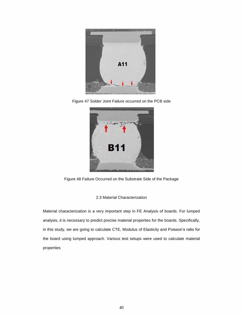
40
Figure 47 Solder Joint Failure occurred on the PCB side
Figure 48 Failure Occurred on the Substrate Side of the Package
2.3 Material Characterization
Material characterization is a very important step in FE Analysis of boards. For lumped
analysis, it is necessary to predict precise material properties for the boards. Specifically,
in this study, we are going to calculate CTE, Modulus of Elasticity and Poisson’s ratio for
the board using lumped approach. Various test setups were used to calculate material
properties

41
Figure 49 TMA and DMA sample
2.3.1 Thermo-Mechanical Analyzer (TMA)
TMA is a device with a thermal chamber which has a good working range of temperature.
TMA is used to measure in-plane and out of plane CTE of the different boards. For this
experiment sample is prepared using High-Speed Cutter, samples are typically cut into 8
by 8 mm of a square shape. The samples are cut to such a dimension that it should sit
below the probe inside the thermal chamber. The probe of the TMA is of Quartz, which
seats on the sample and relative movement of probe gives the CTE plot. CTE can be
calculated for a temperature range of -65°C to 260°C, with a temperature increment of
3°C/min. Three experiments were performed for each measurement and the average value
was taken.

42
Figure 50 Thermomechanical analyzer (TMA),
Figure 51 Universal Testing Machine (UTM)
CTE is measured using TMA in all direction. The out of plane CTE for both the PCB board
is shown in plot 1. Placing PCBs sample in different orientation under TMA’s quartz probe,
we can measure CTE in a different direction. For example, in-plane CTE result is shown
in figure 52. All measurements are done for temperature range -65°C to 260°C, so it can
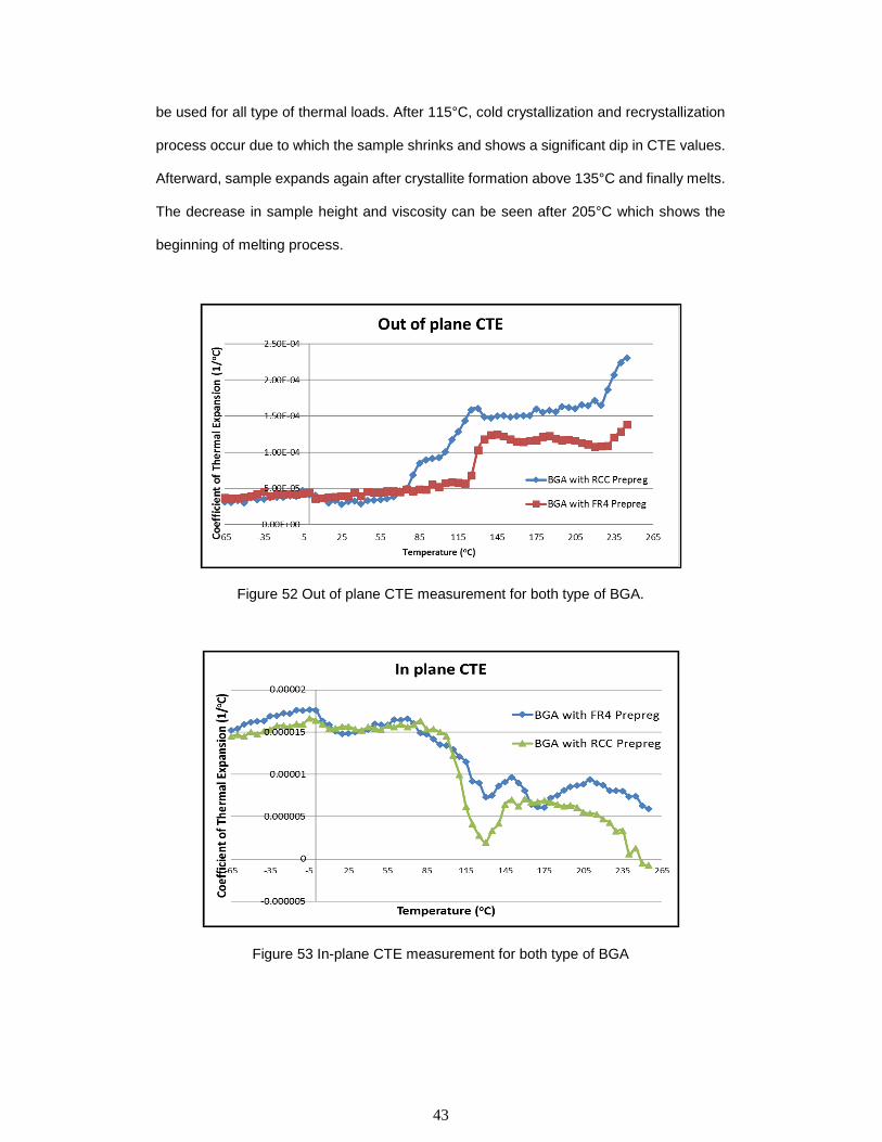
43
be used for all type of thermal loads. After 115°C, cold crystallization and recrystallization
process occur due to which the sample shrinks and shows a significant dip in CTE values.
Afterward, sample expands again after crystallite formation above 135°C and finally melts.
The decrease in sample height and viscosity can be seen after 205°C which shows the
beginning of melting process.
Figure 52 Out of plane CTE measurement for both type of BGA.
Figure 53 In-plane CTE measurement for both type of BGA

44
2.3.2 Universal Testing Machine (UTM)
UTM is a tensile testing machine which was used to calculate the modulus of elasticity and
Poisson’s Ratio of the boards at room temperature. Sample preparation was done by
cutting the boards in dog-bone shaped as per the ASTM D412 Standards. The length of
the dog bone sample was 100mm with the width of 16mm. The length in the middle section
was 33mm and the grip section was 30mm. A force per unit length of magnitude 2 N/m is
applied to the samples. The sample was held in two jaws to carry out the experiment.
Extensometer was placed at the center of dog bone sample during a tensile test and the
lateral deformation was measured to calculate Poisson’s ratio.
Table 4 BGA Package material properties
Material CTE (ppm/°C) E (GPa)
Copper pad 17 11
Die Attach 65 1.54
Die 2.9 150
Mold 8 24
Pi Layer 35 3.3
Solder Mask 30 41.37
All the measured values were temperature dependent. For computational analysis, all
values for PCB was taken as temperature dependent for accuracy. The average fit value
for CTE and Young’s modulus are given in table 2.

45
Table 5 BGA PCB board material properties
Boards CTE (ppm/°C) E (GPa)
x-dir y-dir z-dir
PCB with RCC Prepreg 15.7 15.7 24.2 27.8
PCB with FR4 Prepreg 17.1 17.1 30.5 28.5
2.3.3 Dynamic Mechanical Analyzer
Figure 54 Dynamic Mechanical Analyzer
Figure 55 DMA 3-point bending attachment
46
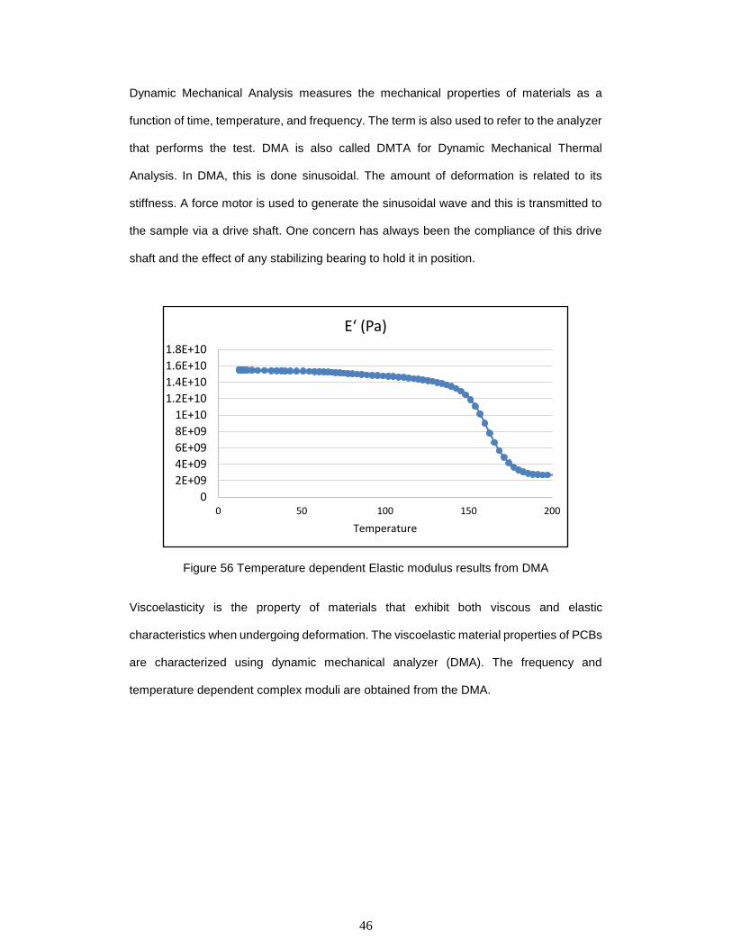
Dynamic Mechanical Analysis measures the mechanical properties of materials as a
function of time, temperature, and frequency. The term is also used to refer to the analyzer
that performs the test. DMA is also called DMTA for Dynamic Mechanical Thermal
Analysis. In DMA, this is done sinusoidal. The amount of deformation is related to its
stiffness. A force motor is used to generate the sinusoidal wave and this is transmitted to
the sample via a drive shaft. One concern has always been the compliance of this drive
shaft and the effect of any stabilizing bearing to hold it in position.
Figure 56 Temperature dependent Elastic modulus results from DMA
Viscoelasticity is the property of materials that exhibit both viscous and elastic
characteristics when undergoing deformation. The viscoelastic material properties of PCBs
are characterized using dynamic mechanical analyzer (DMA). The frequency and
temperature dependent complex moduli are obtained from the DMA.
0
2E+09
4E+09
6E+09
8E+09
1E+10
1.2E+10
1.4E+10
1.6E+10
1.8E+10
0 50 100 150 200
Temperature
E‘ (Pa)
47
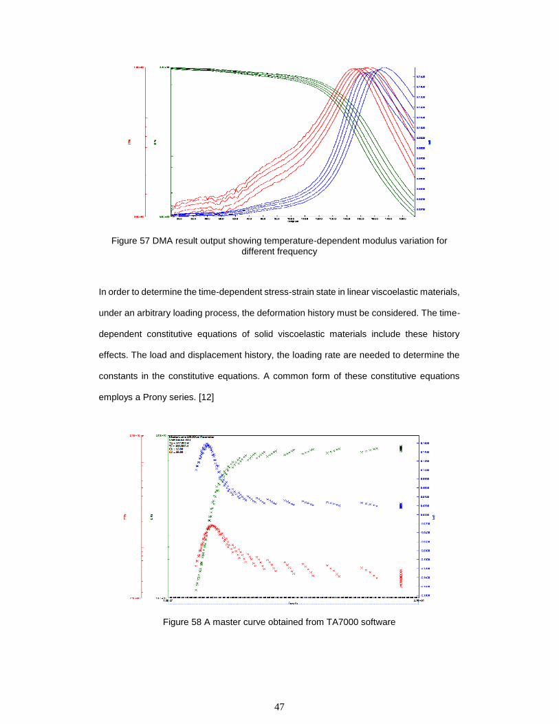
Figure 57 DMA result output showing temperature-dependent modulus variation for different frequency
In order to determine the time-dependent stress-strain state in linear viscoelastic materials,
under an arbitrary loading process, the deformation history must be considered. The time-
dependent constitutive equations of solid viscoelastic materials include these history
effects. The load and displacement history, the loading rate are needed to determine the
constants in the constitutive equations. A common form of these constitutive equations
employs a Prony series. [12]
Figure 58 A master curve obtained from TA7000 software
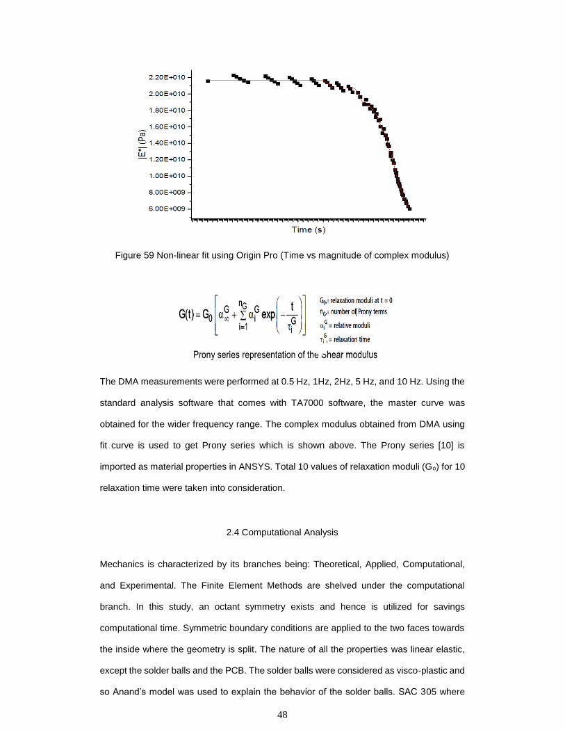
48
Figure 59 Non-linear fit using Origin Pro (Time vs magnitude of complex modulus)
The DMA measurements were performed at 0.5 Hz, 1Hz, 2Hz, 5 Hz, and 10 Hz. Using the
standard analysis software that comes with TA7000 software, the master curve was
obtained for the wider frequency range. The complex modulus obtained from DMA using
fit curve is used to get Prony series which is shown above. The Prony series [10] is
imported as material properties in ANSYS. Total 10 values of relaxation moduli (Go) for 10
relaxation time were taken into consideration.
2.4 Computational Analysis
Mechanics is characterized by its branches being: Theoretical, Applied, Computational,
and Experimental. The Finite Element Methods are shelved under the computational
branch. In this study, an octant symmetry exists and hence is utilized for savings
computational time. Symmetric boundary conditions are applied to the two faces towards
the inside where the geometry is split. The nature of all the properties was linear elastic,
except the solder balls and the PCB. The solder balls were considered as visco-plastic and
so Anand’s model was used to explain the behavior of the solder balls. SAC 305 where
49
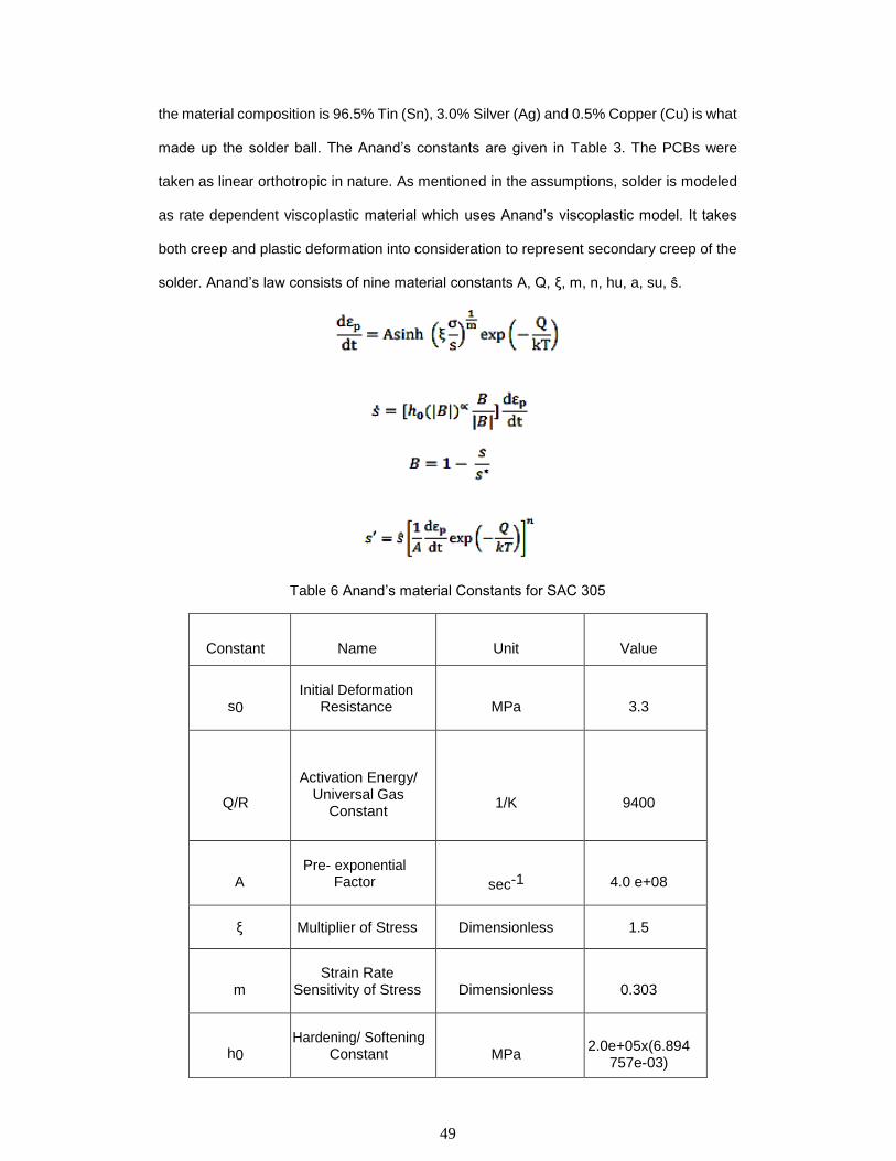
the material composition is 96.5% Tin (Sn), 3.0% Silver (Ag) and 0.5% Copper (Cu) is what
made up the solder ball. The Anand’s constants are given in Table 3. The PCBs were
taken as linear orthotropic in nature. As mentioned in the assumptions, solder is modeled
as rate dependent viscoplastic material which uses Anand’s viscoplastic model. It takes
both creep and plastic deformation into consideration to represent secondary creep of the
solder. Anand’s law consists of nine material constants A, Q, ξ, m, n, hu, a, su, ŝ.
Table 6 Anand’s material Constants for SAC 305
Constant
Name
Unit
Value
s0
Initial Deformation Resistance
MPa
3.3
Q/R
Activation Energy/
Universal Gas Constant
1/K
9400
A
Pre- exponential Factor
sec-1
4.0 e+08
ξ Multiplier of Stress Dimensionless 1.5
m
Strain Rate Sensitivity of Stress
Dimensionless
0.303
h0
Hardening/ Softening Constant
MPa
2.0e+05x(6.894
757e-03)

50
ŝ
Coefficient of Deformation Resistance Saturation
MPa
2.0e+05x(6.894757e-03)
n
Strain Rate
Sensitivity of Saturation
Dimensionless
0.07
a
Strain Rate of Sensitivity of Hardening or
Softening
Dimensionless
1.3
2.5 Methodology & Meshing Meshing is one of the most critical steps in the FEA. Larger the number of elements results
in the better approximation in the solution. Excess number of elements may cause around
off error in some of the cases. To avoid this error the meshing should be fine or coarse in
appropriate region. Mesh sensitivity analysis can be considered to reduce the
computational time while maintaining the accuracy in the solution. Here in this study
different methods are used to mesh the model with fine elements while maintaining the
connectivity between the elements. Initially the meshing is done with a set of elements and
later the number of elements is doubled and compared. If the results are close enough the
initial configuration is used to solve the model to save the computational time. If the solution
is different for both the cases, then mesh refinement is done until the results
are converged [10]. Different types of elements are used such as 2D and 3D elements
based on the application of the analysis.
Basically, to get a detailed stress strain contours near the critical parts of the body sub
modeling is done. In some cases, it may occur that the mesh is too coarse to provide the
better results near the critical areas of the object where the stress is higher. Sub modeling
is also known as local global analysis or cut –boundary displacement method. Cut
51
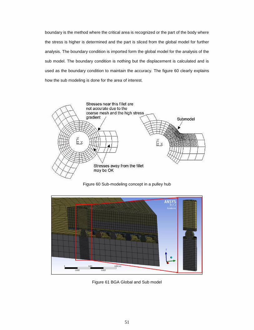
boundary is the method where the critical area is recognized or the part of the body where
the stress is higher is determined and the part is sliced from the global model for further
analysis. The boundary condition is imported form the global model for the analysis of the
sub model. The boundary condition is nothing but the displacement is calculated and is
used as the boundary condition to maintain the accuracy. The figure 60 clearly explains
how the sub modeling is done for the area of interest.
Figure 60 Sub-modeling concept in a pulley hub
Figure 61 BGA Global and Sub model

52
Figure 62 BGA model mesh sensitive analysis plot
Detailed stress-strain contours near the critical parts of the body sub modeling are done.
In some cases, it may occur that the mesh is too coarse to provide the better results near
the critical areas of the object where the stress is higher. Sub-modeling is also known as
local global analysis or cut –boundary displacement method. The cut boundary is the
method where the critical area is recognized or the part of the body where the stress is
higher is determined and the part is sliced from the global model for further analysis. The
boundary condition is imported from the global model for the analysis of the sub model.
Here also, the sub-modeling technique was used for analysis. The detailed global model
was created. [1] [5] A submodel from the global model is sliced as shown in figure 61. The
impact of thermal load is highly active on the corner solder ball. The submodel was created
as shown in figure 61 which includes half corner solder ball. Coarse mesh simulation is
done for global model and cut boundary constraint is imported to submodel where mesh
sensitive analysis was done. The figure 63 shown below is the imported boundary
condition on the connected surface.[3] [4]
575000
580000
585000
590000
595000
600000
605000
610000
615000
0 5000 10000 15000 20000 25000 30000 35000
Pla
stic
wo
rk
Number of elements
Mesh Sensitive Analysis

53
Figure 63 Cut boundary condition from global model
Thermal cycling loading was applied for -40°C to 125°C. A total of three cycles with a
complete cycle of 60min, with 15min ramp and 15min dwell, were applied and the
temperature profile is shown in plot 64.
2.6 Load & Boundary Conditions The Boundary imposed on the global model is shown in the figure. Since the octa
symmetric model in used the faces are applied with symmetry boundary condition. The
center node is fixed i.e., Uz = 0, to prevent rigid body motion. The thermal condition used
for the simulation is the same thermal condition used to obtain the BLR data. The
temperature profile used is shown in the figure below. The simulation is run for over
compete three cycles to obtain a stable stress-strain hysteresis loop. The initial stress free
temperature is set to the room temperature i.e., 25oC.
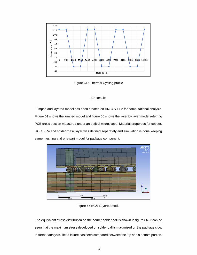
54
Figure 64 : Thermal Cycling profile
2.7 Results
Lumped and layered model has been created on ANSYS 17.2 for computational analysis.
Figure 61 shows the lumped model and figure 65 shows the layer by layer model referring
PCB cross section measured under an optical microscope. Material properties for copper,
RCC, FR4 and solder mask layer was defined separately and simulation is done keeping
same meshing and one-part model for package component.
Figure 65 BGA Layered model
The equivalent stress distribution on the corner solder ball is shown in figure 66. It can be
seen that the maximum stress developed on solder ball is maximized on the package side.
In further analysis, life to failure has been compared between the top and a bottom portion.

55
Figure 66 Equivalent stress on corner solder joint
Figure 67 is the comparison of Von Mises maximum equivalent stress developed on the
corner solder ball for PCB board with RCC and FR4 prepreg. The chart also shows the
comparison of lumped and layer by layer model. Layer by layer model is more defined due
to consideration of PCB content, therefore it shows more stresses and accurate stress
value. The developed stress is less in PCB with RCC prepreg and laminate. The same
trend can be seen in the layered model also but the difference in the value is less.
Figure 67 von-Mises equivalent stress for RCC & FR4 prepreg in lumped and layered model
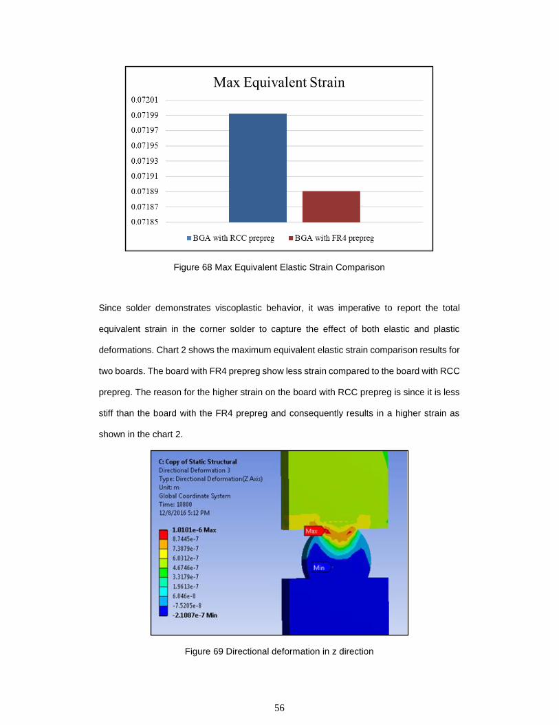
56
Figure 68 Max Equivalent Elastic Strain Comparison
Since solder demonstrates viscoplastic behavior, it was imperative to report the total
equivalent strain in the corner solder to capture the effect of both elastic and plastic
deformations. Chart 2 shows the maximum equivalent elastic strain comparison results for
two boards. The board with FR4 prepreg show less strain compared to the board with RCC
prepreg. The reason for the higher strain on the board with RCC prepreg is since it is less
stiff than the board with the FR4 prepreg and consequently results in a higher strain as
shown in the chart 2.
Figure 69 Directional deformation in z direction

57
The directional deformation along the z-axis is shown in figure 69. It is observed that the
maximum deformation is at top of the corner solder ball. The lumped model is tested and
maximum directional deformation is obtained. The values for RCC and FR4 prepreg board
were compared and are shown in figure 70. The board with FR4 prepreg shows less
deformation in all direction compared to RCC prepreged board. Slit difference in
deformation between x and y-direction is because temperature dependent CTE of the
board in x and y are not identical.
Figure 70 Maximum directional deformation in all axis
Figure 71 Non-linear plastic work distribution on Top portion of corner solder ball

58
Figure 72 Non-linear plastic work distribution on Bottom portion of corner solder ball
Figure 71, 72 shows two portions of corner solder ball. Fig 71 is the top portion which
shows maximum stresses and Fig 72 is also considered for FEA, from experiments and
literature review, it has been seen that even bottom portion has the possibility of crack
propagation. So we have considered both top and the bottom portion of the corner solder
ball to calculate average plastic work. Nonlinear plastic work on the top and the bottom
portion of the solder ball is shown in figure 71, 72.
As seen from the results, the board with FR4 prepreg has less strain, but more Von Mises
stress as compared to the board with RCC prepreg which has a higher strain and less Von
Mises stress. Volume average change in Plastic work between cycle 2 and 3 was
calculated for both the boards using Darveaux’s APDL code. [8] The stiffness of the board
plays a significant role in reliability testing, the number of cycles to failure decreases as
stiffness increases. [11]
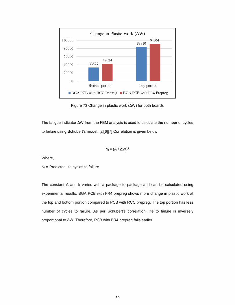
59
Figure 73 Change in plastic work (ΔW) for both boards
The fatigue indicator ΔW from the FEM analysis is used to calculate the number of cycles
to failure using Schubert’s model. [2][6][7] Correlation is given below
Nf = (A / ΔW) k
Where,
Nf = Predicted life cycles to failure
The constant A and k varies with a package to package and can be calculated using
experimental results. BGA PCB with FR4 prepreg shows more change in plastic work at
the top and bottom portion compared to PCB with RCC prepreg. The top portion has less
number of cycles to failure. As per Schubert's correlation, life to failure is inversely
proportional to ΔW. Therefore, PCB with FR4 prepreg fails earlier
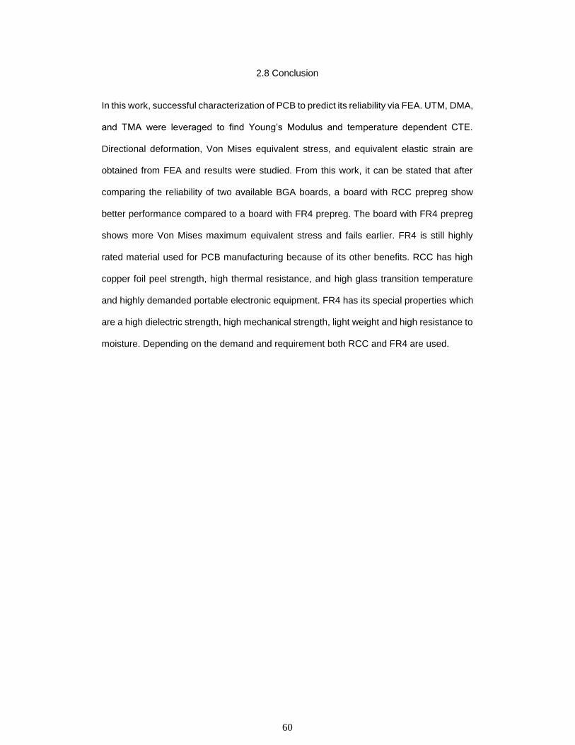
60
2.8 Conclusion
In this work, successful characterization of PCB to predict its reliability via FEA. UTM, DMA,
and TMA were leveraged to find Young’s Modulus and temperature dependent CTE.
Directional deformation, Von Mises equivalent stress, and equivalent elastic strain are
obtained from FEA and results were studied. From this work, it can be stated that after
comparing the reliability of two available BGA boards, a board with RCC prepreg show
better performance compared to a board with FR4 prepreg. The board with FR4 prepreg
shows more Von Mises maximum equivalent stress and fails earlier. FR4 is still highly
rated material used for PCB manufacturing because of its other benefits. RCC has high
copper foil peel strength, high thermal resistance, and high glass transition temperature
and highly demanded portable electronic equipment. FR4 has its special properties which
are a high dielectric strength, high mechanical strength, light weight and high resistance to
moisture. Depending on the demand and requirement both RCC and FR4 are used.
61
2.9 Reference
[1] Sanjay Mahesan Revathi, “Experimental and computational analysis on the effect of
PCB layer copper thickness and prepreg layer stiffness”, UT Arlington MS-Thesis May
2015
[2] A. Schubert, R. Dudek, and E. Auerswald, "Fatigue life models for SnAgCu and SnPb
solder joints evaluated by experiments and simulation," in Electronic Components and
Technology Conference (ECTC), New Orleans, 2003.
[3] Pavan Rajamane, Fahad Mirza, “Chip Package Interaction Study to Analyze the
Mechanical Integrity of a 3-D TSV Package” – American Society of Mechanical
Engineering (ASME) Interpack 2015
[4] Subramanian Gowthaman, Unique Rahangdale, “Impact of thermal loading on the
structural integrity of 3D TSV package” Surface Mount Technology Association
SAInternational 2016.
[5] Fahad Mirza, “Compact Modeling Methodology Development for Thermo-Mechanical
Assessment in High-End Mobile Applications–Planar and 3d TSV Packages” the
University of Texas at Arlington Ph.D. Thesis
[6] A. Schubert, R. Dudek, E. Auerswald, A. Gollbardt, B. Michel, H. Reichl, "Fatigue Life
Models for SnAgCu and SnPb Solder Joints Evaluated by Experiments and Simulation,"
in Electronic Components and Technology Conference (ECTC), 2003.
[7] F.X. Che and John H.L. Pang, "Thermal Fatigue Reliability Analysis for PBGA with Sn-
3.8Ag-0.7Cu Solder Joints," in Electronic Components and Technology Conference
(ECTC), 2004
[8] R. Darveaux, "Effect of simulation methodology on solder joint crack growth
correlation," in Electronic Components and Technology Conference (ECTC), Las Vegas,
2000.
[9] Lau, John H., "Effects of Build-up Printed Circuit Board Thickness on the Solder Joint
Reliability of a Wafer Level Chip Scale Package (WLCSP)" in IEEE Transactions on
Components and Packaging Technologies 2002.
[10] Allan F. Bower, “Applied Mechanics of Solids” CRC Press, New York, 2009.
62
[11] Jimil M. Shah, Richard Eiland, Ashwin Siddharth, Dereje Agonafer, “Effects of mineral
oil immersion cooling on IT equipment reliability and reliability enhancements to data
center operations”, ITHERM 2016, Las Vegas, NV.
[12] Tzikang Chen, “Determining Prony Series for a viscoelastic material from time varying
strain data”, NASA/TM-2000-210123 ARL-TR-2206
[13] Jimil M. Shah, Richard Eiland, Ashwin Siddharth, Dereje Agonafer, “Effects of
mineral oil immersion cooling on IT equipment reliability and reliability enhancements to
data center operations”, ITHERM 2016, Las Vegas, NV.
63
Chapter 3: Impact of Power Cycling on Flip Chip Package
3.1 Introduction
Consumer-electronics manufacturers are striving to reduce product size to meet this
demand. Smaller, thinner, and thermally enhanced packages help achieve product
miniaturization. A performance analysis has shown that Ball Grid Array BGA packages
have better thermal performance than dual in-line surface mount technology (SMT)
packages. Other benefits of the BGA packages are low inductance and capacitance, small
package volume, smaller board routing area, and no external leads, compared to
conventional leaded packages. The BGA package is a thermally enhanced standard size
IC package designed to eliminate the use of bulky heat sinks and slugs. This package can
be easily mounted using standard PCB assembly techniques and can be removed and
replaced using standard repair procedures. The BGA package is designed so that the lead
frame die pad (or thermal pad) is exposed on the bottom of the IC. This provides an
extremely low thermal resistance (θJC) path between the die and the exterior of the
package. This device package has gained popularity in the industry because of its superior
thermal and electrical characteristics. The compact size of BGA package makes it an ideal
choice for handheld portable applications and where package performance is required. To
estimate the reliability of the package, an environmental stress test is used to simulate the
end use environment conditions and to uncover specific materials and process related
marginalities that may be experienced during operational life. Joint Electronic Device
Engineering Council (JEDEC) and the Institute for Printed Circuits (IPC) have adapted,
documented and standardized many of the reliability tests.
Solder joint failure is a major concern for a long time. Electronic manufacturing company
is facing a serious problem because of solder joint failure. ATC is widely used for solder
joint assessment in an environmental chamber or through computational analysis. ATC
forces a uniform temperature distribution of the entire package, but it’s not the case in real
time. Die is the main heat source in PCB assembly and it creates a high-temperature
64
environment around solder joints. Power cycling is non-uniform temperature distribution
load generated due to internal heat from die. Due to its non-uniform behavior, it gives the
more realistic result. BGA package is a more heat generating package. The package
dimension and its volume decide the temperature around in ATC whereas, in power
cycling, power is assigned to die which decides the temperature distribution on assembly
[1][2].
3.2 Objective
The main objective of this study is to analyze the solder joint reliability of BGA package
when both power cycling and thermal cycling are applied. To understand the root cause of
the failure in joints and method to improve the mechanical reliability of the package. Printed
circuit board’s thickness also places an important role in package reliability. Here, three
different thick board were used to do a comparative study. The layered model is compared
with lumped model and solder joint reliability were assessed. Finding critical solder joint
and obtaining life to failure for that critical solder has been done.
3.3 Power Cycling
When a device is switched on and switched off several numbers of times, stresses are
induced in the system. This loading condition is called Power Cycling, whereas ATC is
uniformly distributed the thermal load. JEDEC standards are used to follow standards
values. The time per cycle for both loads are different but minimum three thermal cycles
are needed to get correct plastic work of solder joints. [3]
Various numerical integration tools like Finite Element Analysis are used for virtual
qualification to reduce development time and expenses. ATC conditions assume that the
temperature is uniform throughout the assembly for predicting the life of the module.
However, in practical conditions, the assembly is subjected to power cycles which result in
temperature being non-uniform throughout assembly as the die is the only source of heat

65
generation. The difference in CTE between components results in the deformation of the
package. This deformation is different when the package is subjected to ATC.
Figure 74 Power Cycling Profile
3.4 Methodology
Power cycling is applied in transient thermal analysis with a power density of 0.5W/mm3 to
die [1]. Time of one power cycle is 1600 seconds and is applied for 10800 seconds. The
power cycling profile is shown in through the plot in figure 74. Figure 74 shows the coupled
model in ANSYS and figure 75 is the tree of analysis. With the correct boundary conditions,
power cycling is performed in transient thermal analysis and accelerated thermal cycling
in the static structural analysis. The results of the transient thermal analysis are in form of
temperature distribution. This temperature distribution is imported to static structural
analysis as shown in figure 74. The interesting question comes in mind while transferring
this load is that ‘Is my transferred results are time dependent and different for each node?
so, the answer is yes! After importing load to static structural model, we can check the load
for each time.

66
Figure 75 Transient thermal analysis coupled system
Figure 76 Power cycling - analysis tree from ANSYS model

67
Figure 77 Coupled power and thermal cycling profile
3.5 PCB Material Properties
Material characterization is a very important step in FE Analysis of boards. For lumped
approach, it is necessary to predict precise material properties for boards. Specifically, in
this study, we are going to calculate CTE, Modulus of Elasticity and Poisson’s ratio for the
board using lumped approach. Various test setups were used to calculate material
properties
Table 7 five PCBs material properties
CTE (ppm/oC) E (GPa)
PCB
Thickness in
mil
PCB
Thickness in
mm
X Y Z
27mil 0.7mm 18.3 16.7 30.2 25.5
40mil 1.0mm 15.7 15.7 40.4 28.0
62mil 1.61mm 15.5 15.5 39.4 15.3
93mil 2.4mm 16.3 16.3 37.8 13.0
125mil 3.1mm 15.1 12.8 43.8 14.3
134mil 3.4mm 17.5 17.5 32.8 16.1
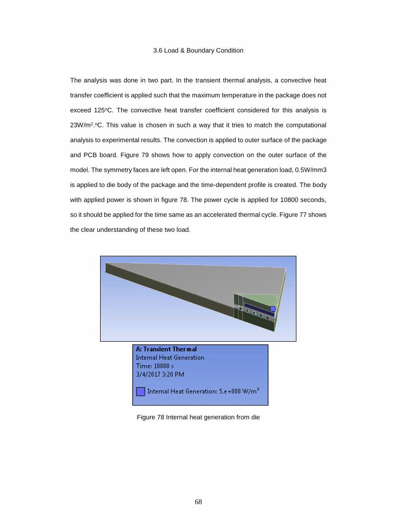
68
3.6 Load & Boundary Condition
The analysis was done in two part. In the transient thermal analysis, a convective heat
transfer coefficient is applied such that the maximum temperature in the package does not
exceed 125oC. The convective heat transfer coefficient considered for this analysis is
23W/m2.oC. This value is chosen in such a way that it tries to match the computational
analysis to experimental results. The convection is applied to outer surface of the package
and PCB board. Figure 79 shows how to apply convection on the outer surface of the
model. The symmetry faces are left open. For the internal heat generation load, 0.5W/mm3
is applied to die body of the package and the time-dependent profile is created. The body
with applied power is shown in figure 78. The power cycle is applied for 10800 seconds,
so it should be applied for the time same as an accelerated thermal cycle. Figure 77 shows
the clear understanding of these two load.
Figure 78 Internal heat generation from die

69
Figure 79 convection on outer surfaces
3.7 Transient Thermal Analysis
A die is the main power source or heat source in power cycling, therefore, a non-uniform
temperature distributed load can be seen on the package. Figure 80 shows the obtained
result from transient thermal analysis. It is the temperature distribution on the octant
symmetry model of BGA package. The maximum temperature is at the die or the junction
and the minimum is at the end of PCB corner.
Figure 80 Temperature distribution due to power cycling

70
Figure 81 output max Temperature (OC) profile from power cycling
Figure 81 shows the maximum temperature profile from power cycling. The total of seven
cycles is applied for 3 hours. As packages get turn on, the temperature starts increasing
for 800 seconds and at the end of dwell time power gets cut off and it cools down due to
convection. The junction temperature for all PCB is shown in 82. The maximum junction
temperature is found be in BGA with 0.7mm thick PCB. The thinner PCB shows lesser
convection from the sides compared to thicker ones. This is only applicable for small
geometries.
Figure 82 max temperature for all PCBs
0
20
40
60
80
100
120
140
0 1800 3600 5400 7200 9000 10800
Time (Sec)
Temperature Profile
100
105
110
115
120
125
130
135
0.7mm 1.0mm 1.61mm 2.4mm 3.1mm 3.4mm
Junction Temperature (o C)
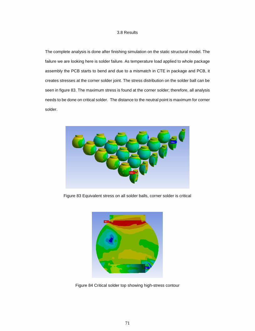
71
3.8 Results
The complete analysis is done after finishing simulation on the static structural model. The
failure we are looking here is solder failure. As temperature load applied to whole package
assembly the PCB starts to bend and due to a mismatch in CTE in package and PCB, it
creates stresses at the corner solder joint. The stress distribution on the solder ball can be
seen in figure 83. The maximum stress is found at the corner solder; therefore, all analysis
needs to be done on critical solder. The distance to the neutral point is maximum for corner
solder.
Figure 83 Equivalent stress on all solder balls, corner solder is critical
Figure 84 Critical solder top showing high-stress contour
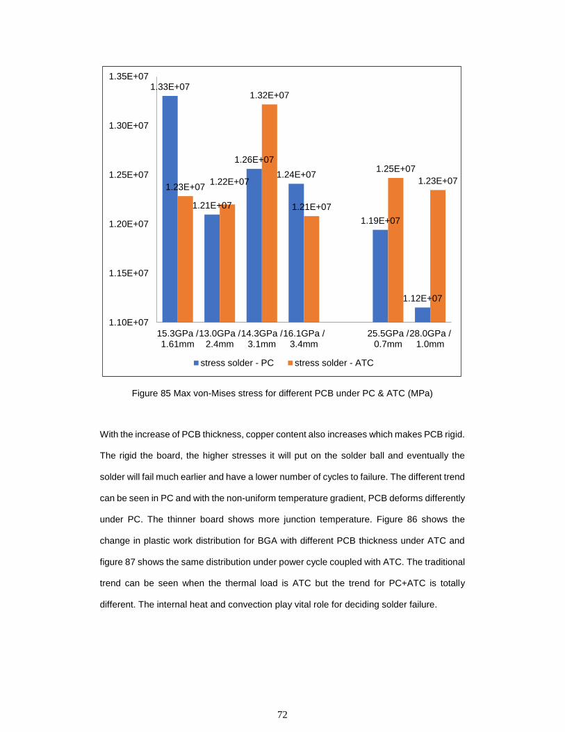
72
Figure 85 Max von-Mises stress for different PCB under PC & ATC (MPa)
With the increase of PCB thickness, copper content also increases which makes PCB rigid.
The rigid the board, the higher stresses it will put on the solder ball and eventually the
solder will fail much earlier and have a lower number of cycles to failure. The different trend
can be seen in PC and with the non-uniform temperature gradient, PCB deforms differently
under PC. The thinner board shows more junction temperature. Figure 86 shows the
change in plastic work distribution for BGA with different PCB thickness under ATC and
figure 87 shows the same distribution under power cycle coupled with ATC. The traditional
trend can be seen when the thermal load is ATC but the trend for PC+ATC is totally
different. The internal heat and convection play vital role for deciding solder failure.
1.33E+07
1.21E+07
1.26E+07
1.24E+07
1.19E+07
1.12E+07
1.23E+071.22E+07
1.32E+07
1.21E+07
1.25E+07
1.23E+07
1.10E+07
1.15E+07
1.20E+07
1.25E+07
1.30E+07
1.35E+07
15.3GPa /1.61mm
13.0GPa /2.4mm
14.3GPa /3.1mm
16.1GPa /3.4mm
25.5GPa /0.7mm
28.0GPa /1.0mm
stress solder - PC stress solder - ATC
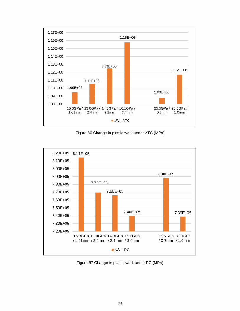
73
Figure 86 Change in plastic work under ATC (MPa)
Figure 87 Change in plastic work under PC (MPa)
1.09E+06
1.11E+06
1.13E+06
1.16E+06
1.09E+06
1.12E+06
1.08E+06
1.09E+06
1.10E+06
1.11E+06
1.12E+06
1.13E+06
1.14E+06
1.15E+06
1.16E+06
1.17E+06
15.3GPa /1.61mm
13.0GPa /2.4mm
14.3GPa /3.1mm
16.1GPa /3.4mm
25.5GPa /0.7mm
28.0GPa /1.0mm
∆W - ATC
8.14E+05
7.70E+05
7.66E+05
7.40E+05
7.88E+05
7.39E+05
7.20E+05
7.30E+05
7.40E+05
7.50E+05
7.60E+05
7.70E+05
7.80E+05
7.90E+05
8.00E+05
8.10E+05
8.20E+05
15.3GPa/ 1.61mm
13.0GPa/ 2.4mm
14.3GPa/ 3.1mm
16.1GPa/ 3.4mm
25.5GPa/ 0.7mm
28.0GPa/ 1.0mm
∆W - PC

74
3.9 Summary and Conclusion
This study shows some interesting results from power cycling analysis. The plastic work
induced in the solder joints is assessed by subjecting the package through PC+ATC.
Plastic work can be used to estimate the number of cycles it requires to initiate and
propagate the crack inside the solder joint. The analysis includes solving a model with the
octant symmetry BGA model under PC+ATC. It is observed that the number of cycles to
failure increases with increase in thickness under PC+ATC whereas per general trend and
our analysis, under only ATC the life to failure decreases with increase in thickness of the
PCB boards. In power cycling, the temperature distribution is non-uniform and therefore
the stress distribution is also different. The package on top of PCB generating heat creates
more deformation in x and y-direction. Many analyses consider only power cycling but for
more realistic analysis and better result, power cycling and ATC should be applied in
combined. The results of the analysis show a significant change in the trend of the failure
in solder joints. Depending on the package power and convection, the results can be
different. The package geometry can affect the convection process. Many parameters are
involved in the computational study of power cycling analysis, therefore, this results could
not be considered as a universal trend. Being close to package or heat generating die,
power cycling shows more damage to the solder joint. Therefore, this test method could
be an important aspect in reliability assessment of solder joints.

75
3.10 Reference
[1] Izhar Z. Ahmed, S. B. Park, “An accurate assessment of interconnect fatigue life through
power cycling” Inter Society Conference on thermal Phenomena 2004.
[2] Jue Li, “Numerical Simulations for Reliability Assessment of Lead- Free Solder
Interconnections in BGA Packages” Aalto University Publications, Department of
Electronics – Doctoral Dissertations 2011.
[3] Bryan Rogers, Jeff Punch, John Jarvis, Pirkka Myllykoski, Tommi Reinikainen, “Finite
Element Modelling of a BGA Package Subjected to Thermal and power cycling” Inter
Society Conference on thermal Phenomena 2012.
[4] Tejas Shetty, “Board Level Reliability Assessment of Thick FR-4 QFN Assemblies
under Thermal Cycling” UT Arlington MS Thesis
[5] Pavan Rajmane, Fahad Mirza, “Chip Package Interaction Study to Analyze the
Mechanical Integrity of a 3-D TSV Package” - ASME Interpack 2015
[6] Subramanian Gowthaman, Unique Rahangdale, “Impact of thermal loading on the
structural integrity of 3D TSV package” Surface Mount Technology Association
International 2016.
[7] Fahad Mirza, “Compact Modeling Methodology Development for Thermo-Mechanical
Assessment in High-End Mobile Applications–Planar and 3d TSV Packages” UT Arlington
Ph.D. Thesis
[8] A. Schubert, R. Dudek, E. Auerswald, A. Gollbardt, B. Michel, H. Reichl, "Fatigue Life
Models for SnAgCu and SnPb Solder Joints Evaluated by Experiments and Simulation,"
in Electronic Components and Technology Conference (ECTC), 2003.
[9] F. X. Che and John H. L. Pang, "Thermal Fatigue Reliability Analysis for PBGA with
Sn-3.8Ag-0.7Cu Solder Joints," in Electronic Components and Technology Conference
(ECTC), 2004
[10] J. Zhao, V. Gupta, A. Lohia and D. Edwards, "Reliability Modeling of Lead-Free solder
joints in wafer level chip scale package," in Journal of Electronic Packaging, 2010
76
[11] R. Darveaux, "Effect of simulation methodology on solder joint crack growth
correlation," in Electronic Components and Technology Conference (ECTC), Las Vegas,
2000.
77
Future Work
[1]. Different die stack can be studied. In this study, 2 die stack model was used for
analysis but 3D packages have different geometry. How the different structure can
affect the solder bump reliability and TSV reliability needs to be analyzed.
[2]. Not just the whole global model even different TSV design could be tried for
reliability enhancement of 3D packages. The material used for TSV and solder
bumps, this all factors are important in package reliability.
[3]. The two parts of this work can be combined which is performing power cycling on
the 3D package. The 3D package is designed in such way that it should produce
more power in small space which will lead to higher probability of solder failures,
thermal cycling has been in used for a long time to investigate the reliability of
packages but the failure due to internal heat need to study for the 3D package.
[4]. Perform CFD analysis for power cycling to identify actual heat transfer coefficient.
ANSYS IcePak or fluent needs to be leveraged for performing CFD analysis.
[5]. Power cycling shows unexpected failure pattern and to validate the computation
work, it needs to be validated by performing experimental power cycling. DC power
unit and Power function generator can be used to create different power cycle
profile.
78
Biographical Statement
Unique Rahangdale received his Bachelor’s degree in Mechanical Engineering from
University of Pune, India, in the year 2015. He pursued his Master’s in Mechanical
Engineering in University of Texas at Arlington from Fall 2015. He joined the Electronics
MEMS & Nanoelectronics Systems Packaging Center (EMNSPC) under Dr. Dereje
Agonafer in 2015 and developed a keen interest in reliability and failure analysis of
electronic packages. His research interest includes reliability, fracture mechanics, thermo-
mechanical simulation and material characterization. Due to his significant contribution in
EMNSPC lab, he received EMNSPC scholarship award in August 2016. During his
graduate studies, he was an integral part of the SRC-funded project where he worked
closely with the industry liaisons. As a Vice-President of Surface Mount Technology
Association (SMTA) UT Arlington student chapter, he was actively involved in all the events
and a technical meeting of SMTA. Unique Rahangdale is author and co-author of more
than 10 research papers published in well-known technical conferences. Upon graduation,
Unique Rahangdale plans to pursue his career in the field of electronic packaging, mainly
focusing on electronic components reliability and analysis.