Status of the CMOS Image Sensor Industry 2017 - Report by Yole Developpement
Upload
yole-developpementCategory
view
9.792download
4
© 2015
Authors: P. Cambou JL. Jaffard
Report publication date: January 2015
From Technologies
to Market
Status of theCMOS image sensor
industry2015 report
© 2015
Courtesy of Omnivision
Courtesy of Valeo
Courtesy of On Semi
Courtesy of Gopro
Courtesy of Sony

2©2015 | www.yole.fr | Status of the CMOS image sensor industry
• WHAT WE GOT RIGHT, WHAT WE GOT WRONG
Over the years Yole Développement has kept consistent forecast
Looking back at previous forecast exercises, Yole Développement has slightly undervalued global CIS market.
The same markets have been researched over time, some new applications such as tablets have impacted the growth.
We have achieved our goal of +/-
10% forecast
Yole Développement © January 2015
-
2,000
4,000
6,000
8,000
10,000
12,000
14,000
16,000
18,000
2007 2008 2009 2010 2011 2012 2013 2014 2015 2016 2017 2018 2019 2020
Reve
nue (
$M
)
Historical revenue forcast (in $M)
2010 Fcst 2012 Fcst 2014 Fcst 2015 Fcst

3©2015 | www.yole.fr | Status of the CMOS image sensor industry
4TH CMOS IMAGE SENSOR REPORT
• When Yole Développement presented its first report in 2010, the imaging industry was at a turning point as CMOSimage sensor revenues were breaking the 50% threshold in respect to CCD.
• Since this first report, Yole documented the rise of a new CIS technology called BSI. In 2015, the 50% revenuethreshold is also broken for BSI technology.
• Mobile and tablets are currently the key applications for CIS, they are demanding in term of volume andperformances therefore keeping price at a good level for the top notch technology. The industry has reached $8.9Bin 2014 and with 10.6% CAGR forecasted for the 2014-2020 period, it will reach $16.2B in 2020.
• Currently the most dynamic CIS market is automotive. New features and performance are needed to serve this newmarket. Are we shifting from vision for imaging to vision for sensing ? One thing is certain, every one in the industryis working on it.
Every thing is changing

4©2015 | www.yole.fr | Status of the CMOS image sensor industry
IMAGE SENSORS : TRIPLE DISRUPTION HISTORY
Technologies & markets have changed dramatically over the years
CIS is now the
undisputed image sensor technology
1865 1945 1985 2005 2015 2020
First color
pictures from
emulsion
plates in
1860’sTube
technology
Never took
over Film
Technology x Market Penetration
CCD
technology
Took over
Film in the
2000’s
CMOS
technology
Took over
CCD in 2010
Acceleration : The speed in technology changes doubles every technology shift
Era of Digital
PhotographyEra of Film
Photography
Era of Mobile
Photography
5 years10 years20 years40 years80 years

5©2015 | www.yole.fr | Status of the CMOS image sensor industry
CMOS IMAGE SENSOR APPLICATIONS
Mobile is currently driving CIS markets
Today smartphone main camera
and DSLR are the 2 main CIS
applications
• Smartphone secondary camera adoption made Mobile sub-segment very significant. It should take an even greater importance in the future as their ASP increase.
• Tablets appear to be part of computing, even tough the technology came from Mobile
$3.0B
$1.0B
$0.2B
Today
Consumer
High End
Mobile
Yole Développement © January 2015

6©2015 | www.yole.fr | Status of the CMOS image sensor industry
CMOS IMAGE SENSOR ECOSYSTEM
The industry is currently undergoing massive changes
The restructuring
activity happened
mostly in the fabless
business model
Foundry Fabless Fab-lite IDM
For Sale?
JV
For Sale?
IPO?
IPO?

7©2015 | www.yole.fr | Status of the CMOS image sensor industry
2009 2010 2011 2012 2013 2014e 2015e 2016e 2017e 2018e 2019e 2020e
Industrial/Space/Defence 235 301 199 224 462 259 277 307 338 372 424 485
Security 36 49 62 84 109 140 175 211 250 286 321 353
Medical 12 14 21 22 25 29 34 39 46 55 63 71
Automotive - - 28 51 71 119 212 330 465 569 668 800
Computing 284 291 449 773 1,125 1,219 1,292 1,433 1,442 1,415 1,377 1,310
Consumer 711 874 1,250 1,558 1,511 1,645 1,680 1,675 1,673 1,699 1,768 1,899
Mobile 3,008 3,621 3,785 4,196 4,712 5,460 6,264 7,087 8,017 9,099 10,178 11,339
0
5,000
10,000
15,000
20,000
Reve
nue (
M$)
2009-2020 CIS revenue forecast (in $M)
by market
CIS REVENUE FORECAST 2014-2020
by market (in $M)
Revenue has reached $8.9B in
2014
Growth is expected at
10.6% CAGR
Yole Développement © January 2015
CAGR2014-2020
TOTAL
yoy Growth
• Revenues are dominated by mobile, consumer and computing which represent 91%. of all CIS revenues in 2014.
• Mobile alone represent 60%.
• From 2014 to 2020, global revenue growth will remain at ~10.6% CAGR.
4,286 5,150 5,794 6,910 8,016 8,871 9,934 11,081 12,232 13,495 14,799 16,258
20% 13% 19% 16% 11% 12% 12% 10% 10% 10% 10%

8©2015 | www.yole.fr | Status of the CMOS image sensor industry
CIS MARKET ANALYSIS 2014-2020
Market breakdown
Main player market share
analysis
Market breakdown
analysis in specific
application segments
9©2015 | www.yole.fr | Status of the CMOS image sensor industry
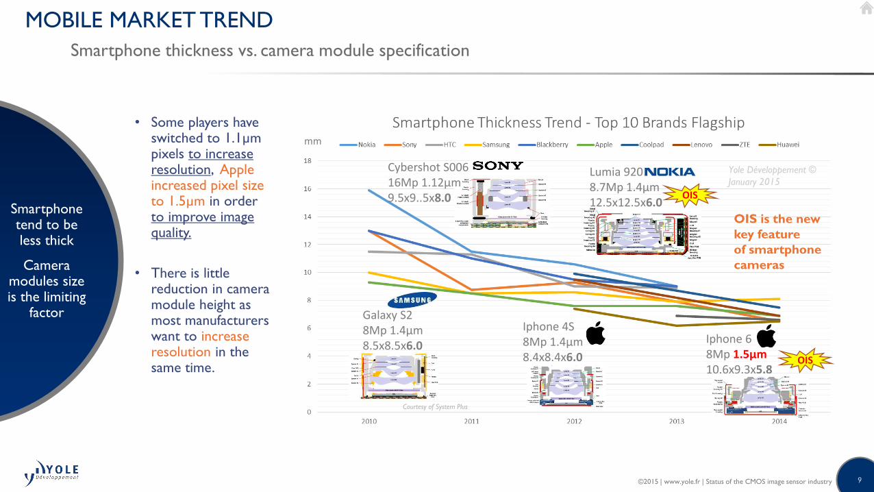
MOBILE MARKET TREND
Smartphone thickness vs. camera module specification
Smartphone tend to be less thick
Camera modules size is the limiting
factor Galaxy S28Mp 1.4µm8.5x8.5x6.0
Lumia 9208.7Mp 1.4µm12.5x12.5x6.0
Iphone 4S8Mp 1.4µm8.4x8.4x6.0
mm
OIS
Iphone 68Mp 1.5µm10.6x9.3x5.8
Yole Développement ©
January 2015
Cybershot S00616Mp 1.12µm9.5x9..5x8.0
Courtesy of System Plus
OIS is the new
key feature
of smartphone
cameras
• Some players have switched to 1.1µm pixels to increase resolution, Apple increased pixel size to 1.5µm in order to improve image quality.
• There is little reduction in camera module height as most manufacturers want to increase resolution in the same time.
OIS

10©2015 | www.yole.fr | Status of the CMOS image sensor industry
MOBILE MARKET TREND
Main rear camera & sub front camera roadmap
The trend is is for more
complexity at the system
level
Log
Image sensor Resolution
2Mp
4Mp
8Mp
16Mp
20182010 2012 2014 2016
Sub CameraResolution VGA-1.2Mp
Pixel size 1.1µm
2020
OIS
Sub CameraResolution 5Mp
Pixel size 1.1µm
Sub CameraResolution 8Mp
Pixel size 1.2µm
Main CamerasResolution 8Mp
Pixel size 1.4µm
OIS
OIS
Main CamerasResolution 8Mp-16Mp
Pixel size 1.1µm- 1.5µm
Main CameraResolution 16Mp+
Pixel size 1.0-1.6µm
Dual CamerasResolution 2x 8Mp
Pixel size 1.1µm+
Size constraints &
Drive for better images &
Features :
→ More pixels
→ Smaller modules
→ Image Stabilization (OIS)

11©2015 | www.yole.fr | Status of the CMOS image sensor industry
AUTOMOTIVE MARKET TREND
From feature to key enabling technology
Challenging use cases are just ramping
up
• 360° surround view
• Dash camera recorder
• Rear view camera
• Night vision
• Cross traffic detection
• Fatigue Warning
• Headlight control
• Traffic sign recognition
• Line departure warning
• Blind spot detection
• Collision avoidance
• Pedestrian detection
• Adaptive speed control
• Highway line keeping
2010 2015 2020
3 to 5 years adoption rate
Feat
ure
Ass
ist
Sem
i-au
to
7 to 10 years adoption rate
10+ years adoption rate
2025
ADAS
1 to 4 Cameras
for Display
1 to 4 Cameras
+ Advanced
image analysis

12©2015 | www.yole.fr | Status of the CMOS image sensor industry
CMOS IMAGE SENSOR TECHNOLOGY
Back side illumination (BSI) is an incremental technology in respect to FSI
• Back side illuminated (BSI) sensors were initially introduced for smart phones. They asked for higher resolution withsame camera module footprint (leading to pixel shrink race) than the pre-existing mobile “feature phones” that hadconventional Front Side Illuminated (FSI) sensors.
• BSI transition is not a disruption like the CCD to CMOS transition. As an incremental improvement over FSI it is nosurprise that a key industry player like Omnivision and Sony were instrumental in bringing this technology to market.The iPhone 4 launch in 2010 was the key turning point for massive BSI adoption.
• BSI technology is now following the same path as basic FSI CIS. As performance improvements get valorised in higherend markets, we can easily forecast a brilliant future of BSI in most market segments.
BSI also started in low end
markets and is moving up

13©2015 | www.yole.fr | Status of the CMOS image sensor industry
Backside
illumination will
enable ~ 100% fill-
factor!
Front-Side
illuminated (FSI)
MAIN TECHNOLOGY TRENDS IN CIS
From FSI to BSI to 3D stacked BSI – pixel level
3D stacked technology is
the logical next step in respect to
BSI
3D Stacked
BSI
Silicon Bulk Silicon Bulk
Backside
illuminated (BSI)
Bonding
Interface
Silicon Bulk
Upper
Wafer
Lower
Wafer
• Conventional BSI is adding a silicon wafer essentially as a mechanical support.
• 3D stacked technology is using a processed wafer with digital circuits supplementing the upper CIS array.

14©2015 | www.yole.fr | Status of the CMOS image sensor industry
Backside
illumination will
enable ~ 100% fill-
factor!
MAIN TECHNOLOGY TRENDS IN CIS
The 3D Stacked BSI could use hybrid bonding in a short future
TSV is the current
interconnection technology
3D Stacked
BSI
Silicon Bulk
TSVTSV
Backside
illumination will
enable ~ 100% fill-
factor!
3D Hybrid
BSI
Silicon Bulk
Interco upper to
lower wafer
Interco upper
to lower wafer
Connection within pixels
become possible
• The key technology step for 3D stack BSI is the interconnection of the upper and lower part of the circuit.
• Currently TSV is the main technology to connect 3D stacked wafers.
• Cu-Cu hybrid bonding should be the next step
• Hybrid bonding could open the way to in pixel connections

15©2015 | www.yole.fr | Status of the CMOS image sensor industry
ABOUT THE AUTORS OF THIS REPORT
Biography & contact
Pierre Cambou
In 1999 Pierre Cambou joined the imaging industry. He had earned an Engineering degree from Université de Technologie de Compiègne in parallel to a Master of Science from Virginia Tech in 1998. More recently he graduated from Grenoble Ecole de Management’s MBA. Pierre took several positions at Thomson TCS which became Atmel Grenoble in 2001 and e2v Semiconductors in 2006. In 2012 he founded the start-up Vence Innovation (now called Irlynx) in order to bring to market a disruptive Man to Machine interaction technology. He joined Yole Développement as Imaging Activity Leader in 2014.
Contact: [email protected]
Jean-Luc Jaffard
From 1966 Jean-Luc Jaffard paved the way of imaging activity at STMicroelectronics being at the forefront of the emergence and growth of this business. At STMicroelectronics Imaging Division he was successively appointed Research Development and Innovation Director managing a large multidisciplinary and multicultural team and later on promoted Deputy General Manager and Advanced Technology Director in charge of identifying and developing breakthrough Imaging Technologies and to transform them into innovative and profitable products. In 2010 he was appointed STMicroelectronics Intellectual Property Business UnitDirector. In January 2014 he created the Technology and Innovation branch of Red Belt Conseil.

17©2015 | www.yole.fr | Status of the CMOS image sensor industry
MEMS &
Sensors
LED / OLED
Compound
Semi.
Imaging Photonics
MedTech
Manufacturing
Advanced
PackagingPV
Power
Electronics
FIELDS OF EXPERTISE
Yole Développement’s 30 analysts operate in the following areas

18©2015 | www.yole.fr | Status of the CMOS image sensor industry
4 BUSINESS MODELS
o Consulting and Analysis
• Market data & research, marketing analysis
• Technology analysis
• Strategy consulting
• Reverse engineering & costing
• Patent analysis
www.yole.fr
o Reports
• Market & Technology reports
• Patent Investigation and patent infringement risk analysis
• Teardowns & Reverse Costing Analysis
• Cost Simulation Tool
www.i-Micronews.com/reports
o Financial services
• M&A (buying and selling)
• Due diligence
• Fundraising
• Maturation of companies
• IP portfolio management & optimization
www.yolefinance.com
Blu Morpho
o Media
• i-Micronews.com website
• @Micronews e-newsletter
• Technology magazines
• Communication & webcast services
• Events
www.i-Micronews.com

19©2015 | www.yole.fr | Status of the CMOS image sensor industry
A GROUP OF COMPANIES
Market,
technology and
strategy
consulting
www.yole.fr
M&A operations
Due diligences
www.yolefinance.com
Fundraising
Maturation of companies
IP portfolio management & optimization
TBA
Manufacturing costs analysis
Teardown and reverse engineering
Cost simulation tools
www.systemplus.fr
IP analysis
Patent assessment
www.knowmade.fr
Blu Morpho

20©2015 | www.yole.fr | Status of the CMOS image sensor industry
OUR GLOBAL ACTIVITY
Yole JapanYole Inc.
Yole
Korea
40% of our business is in
EU countries30% of our business is in
North America
30% of our business is in
Asia
Blu Morpho

21©2015 | www.yole.fr | Status of the CMOS image sensor industry
RESEARCH PRODUCTS - CONTENT COMPARISON
Custom analysis scope is defined with
you to meet your information and
budget needs
Breadth of the analysis
Dep
th o
f th
e a
naly
sis
Custom
Analysis
Workshops
Standard Reports

22©2015 | www.yole.fr | Status of the CMOS image sensor industry
SERVING THE ENTIRE SUPPLY CHAIN
Our analysts provide market analysis,
technology evaluation,
and business plan along the entire
supply chain
Integrators and
end-users
Device
makers
Suppliers: material,
equipment, OSAT,
foundries…
Financial investors,
R&D centers

23©2015 | www.yole.fr | Status of the CMOS image sensor industry
SERVING MULTIPLE INDUSTRIAL FIELDS
We are workingaccross
multiples industries to understand
the impact of More-than-
Moore technologies from deviceto system
From A to Z…
Transportation
makers
Mobile phone
and consumer
electronics
Automotive
Medical
systemsIndustrial and
defense
Energy

24©2015 | www.yole.fr | Status of the CMOS image sensor industry
REPORTS COLLECTION
o Yole Développement publishes a comprehensive collection of market & technology reports and patent analysis in:
• MEMS & Sensors
• Imaging
• Medical technologies (MedTech)
• Advanced packaging
• Power electronics
• Compound semiconductors
• OLED, LED & Laser diode
• Semiconductor Manufacturing
• Photovoltaics
• Batteries
o Our reports are unmatched in quality and technology depth and typically include:
• Technology trends and evolution: costs, barriers, roadmaps, etc.
• Supply & value chain analysis: business models, relationships, value flows, etc.
• In-depth analysis of applications and market drivers: challenges, inflection points, etc.
• Market data ($, units, wafer starts, etc.)
o Every year, Yole Développement, System Plus Consulting and Knowmade publish +60 reports.
o Take the full benefit from our Bundle and Annual Subscription offers.
www.i-Micronews.com

25©2015 | www.yole.fr | Status of the CMOS image sensor industry
OUR 2015 REPORTS PLANNING
MARKET & TECHNOLOGY REPORTS by Yole Développement
o MEMS & SENSORS
− Sensors and Data Management for Autonomous Vehicles
− AlN Thin Film Markets And Applications
− Sensors for Wearable Electronics And Mobile Healthcare
− Status of the MEMS Industry
− Uncooled IR Imagers
− IR Detectors
− High End Gyro, Accelerometers and IMU
− Non-Volatile Memory
o IMAGING & OPTOELECTRONICS
− Camera Module Packaging (Vol 1 : Market & Technology Trends / Vol 2 Teardowns &
Reverse Engineering)
− Uncooled IR Imagers
− Wafer Level Optics
− Status of the CMOS Image Sensors
− Machine Vision
o MEDTECH
− Microfluidic for Sample Preparation
− Microfluidic Applications
− Sensors for Wearable Electronics And Mobile Healthcare
o COMPOUND SEMICONDUCTORS
− High Purity Alumina (HPA)
− Sapphire
− Wide Bandgap Materials For Power Electronics: SiC, GaN (and also Ga2O3, AlN,
Diamond, Graphene… as a trend)
* Reports to be decided within 2015
o LED
− LED Module
− OLED for Lighting
− UV LED
− LED Phosphors Market
o POWER ELECTRONICS
− Power Packaging
− Thermal Management for LED and Power
− Power Electronics for Renewable Energy
− Energy Management For Smart Grid And Smart Cities
− Status of Chinese Power Electronics Industry
− New Technologies For Data Center
− Inverter Market Trends For 2013 – 2020 And Major Technology Changes*
− IGBT Markets And Application Trends
− Power Electronics for HEV/EV*
− Status of Power Electronics Industry
o ADVANCED PACKAGING
− Advanced Packaging in Emerging Markets in China
− Status of the Advanced Packaging Industry
− Supply Chain Readiness for Panel Manufacturing in Packaging
− WLCSP*
− Flip Chip Business Update
− 2.5D & 3DIC Business Update
− Fan-Out and Embedded Business Update
o MANUFACTURING
− Lithography for MEMS, Advanced Packaging and LED
− Thinning & Dicing Equipment for Advanced Packaging, MEMS, Photovoltaics, LED, CMOS
Image Sensors
− Non-Volatile Memory

26©2015 | www.yole.fr | Status of the CMOS image sensor industry
OUR 2015 REPORTS PLANNING
PATENT ANALYSIS by Knowmadeo Patent Infringement (crossed analysis based on Knowmade and System Plus Analysis expertise)
− MEMS Microphone Applications
− Infrared Imaging
o Patent Investigation (crossed analysis based on Knowmade &Yole Développement expertise)
− Power GaN
− MEMS Gyroscope
− 6-axis & 9-axis Inertial MEMS IMUs
− Microbatteries
− Embedded Active & Passive Packages
− Interposer
− Phosphors for LED
TEARDOWN & REVERSE COSTING by System Plus ConsultingMore than 30 teardowns and reverse costing analysis and cost simulation tools to be published in 2015.
* Reports to be decided within 2015

27©2015 | www.yole.fr | Status of the CMOS image sensor industry
OUR 2014 PUBLISHED REPORTS LIST
MARKET & TECHNOLOGY REPORTS
by Yole Développement
o MEMS & SENSORS
− Technologies & Sensors for the Internet of Things: Businesses & Market Trends 2014-2024
− MEMS Microphone: Market, Applications and Business Trends 2014
− Status of the MEMS industry
− MEMS & Sensors for Mobile Phones and Tablets
− High End Gyroscopes and Accelerometer Applications
− Inertial MEMS Manufacturing Technical Trends
− New Detection Principles & Technical Evolution for MEMS & NEMS
− 6/9 DOF Applications in Consumer Electronics
− MEMS for RF filters and Antena Switches - BAW / SAW
o IMAGING & OPTOELECTRONICS
− Status of the CMOS Image Sensor Industry
− Uncooled Infrared Imaging Technology & Market Trends
− Silicon Photonics
o MEDTECH
− Point of Care Testing: Applications for Microfluidic Technologies
− Solid State Medical Imaging: X-ray and Endoscopy
o COMPOUND SEMICONDUCTORS
− RF GaN Technology & Market Analysis: Applications, Players, Devices & Substrates 2010-
2020
− SiC Modules, Devices and Substrates for Power Electronics Market
− GaN-on-Si Substrate Technology and Market for LED and Power Electronics
− Power GaN Market
− Graphene Materials for Opto & Electronic Applications
− Sapphire Applications and Market: from LED to Consumer Electronics
o LED
− LED Packaging
− LED Front-End Manufacturing Trends
− LED Front-End Equipment Market
o POWER ELECTRONICS
− Power Electronics for HEV/EV
− Inverters
− Gate Driver Unit Market for Power Transistors
o PHOTOVOLTAICS
− Emerging and Innovative Technology Approaches in the Solar Industry
o ADVANCED PACKAGING
− 3DIC Equipment and Materials
− 3DIC & 2.5D TSV Interconnect for Advanced Packaging - 2014 Business Update
o MANUFACTURING
− Market & Technology Trends in Materials & Equipment for Printed & Flexible Electronics
− Permanent Wafer Bonding for Semiconductor: Application Trends & Technology
PATENT ANALYSIS
by Knowmade− LED Based on Nano-wires Patent Investigation
− GaN on Si Patent Investigation (LED, Power devices and RF Devices)
− New MEMS Devices Patent Investigation
− Non Volatile Memory Patent Investigation
TEARDOWN & REVERSE COSTING
by System Plus ConsultingMore than 30 teardowns and reverse costing analysis and cost simulation tools to be published in 2014.

28©2015 | www.yole.fr | Status of the CMOS image sensor industry
MICRONEWS MEDIA
o About Micronews Media
Micronews Media, powered by Yole
Développement, ensures you the best visibility
in the disruptive semiconductor community.
With our services, we help you to reach your
customers worldwide with the media products
they prefer, including our website, e-newsletter,
webcasts, and magazines. Invest in a high added-
value editorial program and get access to Yole
Développement’s network (48 000+ contacts).
o Five supports and channels for your visibility
• A technology magazine to highlight
your visibility with advertisements,
company profiles, product descriptions and
white papers
• A webcast to highlight your expertise and
develop your business identifying
commercial leads
• Articles, advertisements & logo and
banners dedicated to your company, its
products and expertise in @Micronews e-
newsletter and on i-Micronews.com
Focused
community
Identified
contacts
Large
community
Mass contacts

29©2015 | www.yole.fr | Status of the CMOS image sensor industry
COMMUNICATION SERVICES
All services listed below are available on–demand.
o i-Micronews.com, the website
Slider – Banners (on English or Japanese websites) – Articles –
Logo and profile as sponsor
o @Micronews, the e-newsletter
Headline article - Tiles
o Custom webcast
Develop your dedicated event with a high added-value program. A
turnkey event withYole support (logistics, promotion, data…)
o Technology Magazines: Custom – Co-produced
Increase your visibility through a dedicated technology magazine
with ads, company profile, product descriptions and white papers.
It can be a custom magazine: your company is the only one to
benefit from it – or a co-produced one: up to 2 companies.
Contacts:
Camille Veyrier ([email protected]) and Clotilde Fabre ([email protected]),
Media & Communication Coordinators.

30©2015 | www.yole.fr | Status of the CMOS image sensor industry
CONTACT INFORMATION
o Consulting and Specific Analysis
• North America: Steve LaFerriere, Director of Northern America Business Development, Yole Inc.
Email: [email protected]
• Japan: Yutaka Katano, General Manager, Yole Japan & President, Yole K.K.
Email: [email protected]
• RoW: Jean-Christophe Eloy, President & CEO, Yole Développement
Email: [email protected]
o Report business
• North America: Steve LaFerriere, Director of Northern America Business Development, Yole Inc.
Email: [email protected]
• Europe: Fayçal El Khamassi, Headquarter Sales Coordination & Customer Service
Email: [email protected]
• Japan & Asia: Takashi Onozawa, Sales Asia & General Manager, Yole K.K.
Email: [email protected]
• Korea: Hailey Yang, Business Development Manager, Korean Office
Email: [email protected]
o Financial services
• Jean-Christophe Eloy, CEO & President
Email: [email protected]
o General
• Email: [email protected]
Follow us on