Diamond Materials for Semiconductor Applications 2013 Report by Yole Developpement
21
© 2013 Diamond materials for semiconductor applications Will high-frequency and high-power devices benefit from the diamond revolution as a replacement of Si, SiC and GaN…? Dow corning 75, cours Emile ZOLA, F-69100 Villeurbanne, France Tel: +33 472 83 01 80 - Fax: +33 472 83 01 83 Web: http://www.yole.fr YOLE DEVELOPPEMENT
-
Upload
yole-developpement -
Category
Technology
-
view
1.160 -
download
20
description
Will high-frequency and high-power devices benefit from the diamond revolution as a replacement of Si, SiC and GaN? $43M diamond material market in 2020 will be driven mainly by passive devices Diamond materials have been in development for more than 50 years. Besides the traditional tooling applications (drilling, cutting…), the interest in diamond continues to grow for optical and thermal applications, and for new applications in semiconductor devices such as high-power devices and high-frequency devices able to work at elevated temperatures. In fact, diamond’s unique physical and electrical properties, which include: the highest known thermal conductivity, a wide band gap, excellent electrical insulator properties, very high breakdown voltage and very high carrier mobility, make diamond an excellent candidate for electronic devices with ultimate performance. However, the costs of diamond, as well as the remaining technology barriers limit the diamond material market to only a few applications and some high-end devices. The diamond applications in electronic devices, such as high-voltage power electronics, high-frequency high-power devices, and high-power optoelectronic devices (laser diodes, LEDs), are the scope of the report. Both passive (heat spreaders) and active (diodes, transistors) diamond solutions are considered in the market quantification. Despite the high costs of high-quality materials, a large number of players are involved in the 2013 diamond materials market and its largest segment – R&D activities. Two scenarios for 2013-2020 diamond material market growth are presented in the report. According to the base scenario, the diamond materials market for semiconductor devices will surpass $43M and will be represented mainly by heat spreaders used in high-power device thermal management. Access to high-quality diamond material is key for diamond device development Electronic applications, such as Schottky diodes, transistors, etc., require high-quality single-crystalline CVD diamond, which has superior characteristics such as high carrier mobility, long carrier lifetimes, high breakdown fields and high thermal conductivity. High quality low-defect diamond wafers produced from diamond crystal made by High-Pressure High-Temperature (HPHT) method are only a few mm in size. In comparison, the competing semiconductor materials such as SiC are already available in wafer sizes up to 150 mm. For future diamond-based active devices, it is crucial to increase the wafer size above 2-inch with the defect density 100 cm-2 and below. Different approaches to achieve free-standing wafers from thick diamond films are under development. A mosaic type method is currently approaching 2-inch wafer size, but the defect density needs to be reduced. According to our technology roadmap for single crystal diamond wafers... More information on that report at http://www.i-mic
Transcript of Diamond Materials for Semiconductor Applications 2013 Report by Yole Developpement

© 2013
Diamond materials for
semiconductor applications
Will high-frequency and high-power devices benefit from the diamond
revolution as a replacement of Si, SiC and GaN…?
Dow corning
75, cours Emile ZOLA, F-69100 Villeurbanne, France
Tel: +33 472 83 01 80 - Fax: +33 472 83 01 83
Web: http://www.yole.fr
YOLE DEVELOPPEMENT

© 2013 • 2
Overview of diamond applicationsYole Développement
Diamond applicationsApplications of diamond in electronic devices
High-power and high-frequency devices
such as Schottky diodes, transistors…
Heat spreaders for high-power
electronics, laser-diodes…
IR windowsMEMS
UV detectorsAFM tips Cutting, sawing tools
UV LEDs
Electrochemical/bio
chemical sensors
Quantum applications
High-power laser windows Cold cathode emitter
Scope of the report
YOLE DEVELOPPEMENT

© 2013 • 3
Two approaches within the semiconductor technology roadmap for power electronic devicesYole Développement
Semiconductor technology roadmap for
power electronic devices
Si
Diamond
.
Do you see the opportunity in going directly with diamond towards ultimate
applications?
Devic
e p
erf
orm
an
ce
Technology and cost barriers
SiC, GaN
.
YOLE DEVELOPPEMENT

© 2013 • 4
• lnGaN/GaN high electron mobility transistors (HEMTs) are actively pursued for high-speed
and high-power applications.
• However, their performance is limited by the thermal conductivity of the substrates on which
GaN is grown (Si, sapphire, SiC). GaN material itself has very low thermal conductivity.
• Thanks to using a thin layer of CVD diamond with very high thermal conductivity (8-12
W/(cm.K), the device thermal resistance can be significantly reduced, providing possibility
to extract more power from the device (at given frequency and given ambient temperature).
Thinner diamond layer and its better thermal properties compared to silicon makes the use of GaN-on-Diamond approach very promising
for high-power devices.Group4Labs, Yole Développement
Why GaN-on-Diamond for HEMTs?
Si (400 µm)
Diamond (25µm)
Active layers (~20 nm only!)
AlGaN/AlN/GaN epi (~1 µm)
Lower
thickness
Much higher thermal
conductivity
Better power
extraction from
the device
1.5 W/(cm.K)
12 W/(cm.K)YOLE DEVELOPPEMENT

© 2013 • 5
• Despite promising diamond properties, the use of diamond for real applications is
still hampered by its extremely high manufacturing costs.
Comparison of prices of different semiconductor materials Yole Développement, October 2013
Costs of diamond materialsDiamond vs other other semiconductor material
YOLE DEVELOPPEMENT

© 2013 • 6
Diamond Material Market ValueBase scenario
Diamond Material Market forecast 2013-2020 – base scenarioYole Développement
The market of diamond material for electronic applications will reach 43.3 M$ in 2020.
YOLE DEVELOPPEMENT

© 2013 • 7
Diamond R&D and Technology RoadmapHistory of diamond crystal and film development
Diamond technology has been developed since more than 60 years. The achievement
of commercially available diamond-based devices is a long-term run!
1950 1960 1970 1980 1990 2000 2010
>60 years of development
1954
Patent on CVD
diamond growth issued
1954
Xxxxx
xxxx
xxx
(GE)
2007
Xxxxxx
(E6)
1952
Xxxxxxxxxxx
xxxxxxxxxx (Eversole)
2013
Xxxx xxxxxx
(Sumitomo Electric)
1966
Xxxxxx
xxxx
xxxxxx 1981
Xxxxx
xxxxxxxxxxxxx
(Setaka, NRIM)
1983
Xxxx
xxx
xxxxxxxxxx
(Sumitomo Electric)
1994
Xxxxxx
xxxx
E6
2002
Xxxxxxxx
(Argonne laboratory)
YOLE DEVELOPPEMENT
© 2013 • 8
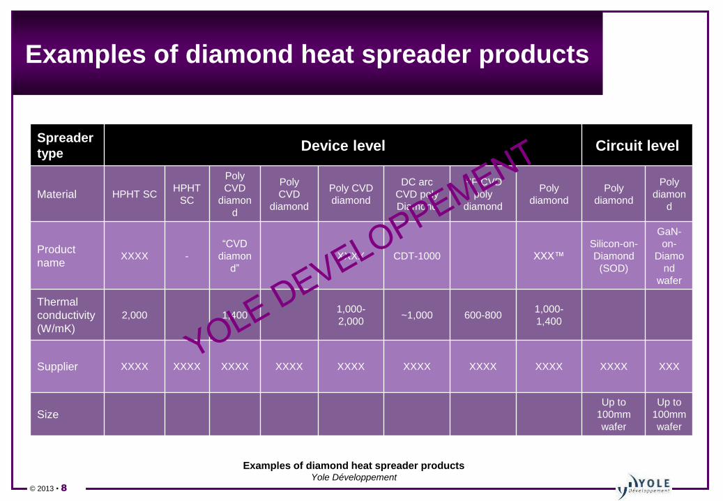
Examples of diamond heat spreader products
Examples of diamond heat spreader productsYole Développement
Spreader
typeDevice level Circuit level
Material HPHT SCHPHT
SC
Poly
CVD
diamon
d
Poly
CVD
diamond
Poly CVD
diamond
DC arc
CVD poly
Diamond
HF CVD
poly
diamond
Poly
diamond
Poly
diamond
Poly
diamon
d
Product
nameXXXX -
“CVD
diamon
d”
XXXX CDT-1000 XXX™
Silicon-on-
Diamond
(SOD)
GaN-
on-
Diamo
nd
wafer
Thermal
conductivity
(W/mK)
2,000 1,4001,000-
2,000~1,000 600-800
1,000-
1,400
Supplier XXXX XXXX XXXX XXXX XXXX XXXX XXXX XXXX XXXX XXX
SizeUp to
100mm
wafer
Up to
100mm
wafer
YOLE DEVELOPPEMENT

© 2013 • 9
Diamond material ASP ($/mm3)
Single-crystal wafer $XX - $X00
Heteroepitaxially-grown diamond wafer Not commercially available yet
Self-standing CVD polycrystalline wafer $X.5 - $X
Comparison of 2013 Average Selling Prices for different diamond materialsYole Développement
ASP of different diamond materials
• The Average Selling Price (ASP) for a given diamond material depends on
numerous factors.
• Large price variations have been therefore observed depending mainly on the
grade of diamond material (mechanical, optical, electronic, electronic+…), wafer
size and thickness and quantity ordered.
YOLE DEVELOPPEMENT

© 2013 • 10
Diamond Material Market DemandAggressive scenario
Diamond Material Demand – aggressive scenario. The demand for R&D purposes is not included here.Yole Développement
YOLE DEVELOPPEMENT

© 2013 • 11
The main barrier in the development of electronic devices based on diamond wafer is a very
small size of diamond wafers and a low number of wafers produced from one single diamond
crystal resulting in very high costs.
Comparison of silicon, SiC and diamond wafer sizes (axis not in scale)Yole Développement
Diamond wafer size is key for diamond active
device development
Wafer size (mm)
Wafe
rs p
er
cry
sta
l
X0 XX0 XX0 XX0
X0
X0
XX0
SiC
XX0X5
Silicon
YOLE DEVELOPPEMENT

© 2013 • 12
Single crystal growthComparison of HPHT and MWCVD techniques for single-crystal
diamond growth
High-Pressure High-Temperature
(HPHT)
Microwave Chemical Vapor
Deposition (MW CVD)
PrincipleReplication of natural diamond growth
conditions deep within the earth, producing
high temperatures and high pressures
Gas-phase synthesis, which activates hydrogen
and methane gas by discharging plasma to grow
diamond on seed crystals
EquipmentPress apparatus able to generate very high
pressures and temperaturesMW CVD reactor
No of crystals per
equipment per growth runX Up to X0
Growth rate Few mm in X days Very small (half a mm per XX)
ProductHigh-purity and low-defect single crystal
diamonds
Large, single crystal diamonds
Thin slabs (<X0µm) available
Crystal size < X0 mm~X0mm x X0mm
Up to XXmm x XXmm using mosaic method
Scalability Very limited Less limited than HPHT
Cost Extreme high Very high (possibility of cost reduction)
Main playersGemesis, Element Six, Sumitomo
Many Chinese players
Indian players (for jewelry)
EDP Corp., Scio Diamond Technology
Corporation, IIa Technologies
Main applicationsJewelry
Substrates for MWCVD crystal growth,
abrasives, cutting and drilling tools…
Industrial applications
Jewelry
YOLE DEVELOPPEMENT

© 2013 • 13
Diamond wafer fabricationDiamond wafer: State-of-the-art
Wafer type Growth technique Size Defect density
Insulating
Wafer
HPHTX to XX mm
(further size increase
very limited)
~10X cm-2
CVDX to XX mm
(potential for further
size increase)
~10X cm-2
Mosaic wafer CVD
XX x XX mm2
XX x XX mm2
(potential for further
size increase)
~10X cm-2
P+ type Wafer HPHT
Wafer CVD
N+ type
Current status of diamond wafer manufacturingYole Développement, AIST
YOLE DEVELOPPEMENT

© 2013 • 14
Gro
wth
rate
High growth rate, needed for diamond film cost reduction, is usually incompatible with high film
quality, thickness uniformity and deposition on large areas.
Comparison of growth rate and deposition area for different diamond film growth techniquesYole Développement
Diamond film growthComparison of different growth techniques
Plasma TorchX0-XX0 µm/h
~X cm2
HF CVD0.X-0.X µm/h
> 0.X m2
Deposition area
MW CVD0.X-X0 µm/h
Ø XX0 mm
Cost reduction
target
YOLE DEVELOPPEMENT

© 2013 • 15
Application
CompanyCrystal grower
Diamond deposition
tool
Diamond
etching
Diamond
processing
Company (US) HF CVD
Company (US) MW CVD
Company (US) MW CVD
Company (Luxembourg) MW CVD
Company (US) HPHT
Company (DE) MW CVD
Company (JP)Ultrahigh pressure
press (in the past)
Company (US) MWCVD MW plasma (ECR)
Company (CH) HF CVD
Company (UK) ICP, RIE
Company (UK)Laser equipment for
precise micromachining
Company (FR) MW CVD
Company (CH) Laser equipment
Company (US) MWCVD (crystal)
Company (US) HF CVD, DC arc plasma jet
Equipment makers and products & activities within the diamond businessYole Développement
Equipment makersOverview
YOLE DEVELOPPEMENT

© 2013 • 16
Diamond R&DEU R&D projects related to diamond applications in electronics
Examples of R&D projects related applications of diamond in electronicsYole Développement
YOLE DEVELOPPEMENT

© 2013 • 17
Company and R&D institution profilesSynthesis
Name Country Founded Employees Business model Products Comments
Company UK 2008 5Private company, development of
diamond based devices
Company UK 1947 2,500Development and manufacturing of
diamond products
HPHT and CVD diamondmaterials for mechanical,
optical and electronicapplications
Non-diamond materials (tungsten carbide, boron
nitride…)
Private companyowned by XXX and
XXX Recently acquired
XXX
Company USA 2003 <10 A fabless start-up companyCVD diamond, GaN on
diamond
Since May 2013 operates as a
subsidiary of XXX
Company USA 1996 NADevelopment and manufacturing of diamond single crystals mainly for
jewelryCut diamonds
Privately heldProprietary HPHT
technology
Company DE 1997 <10Development and manufacturing of
a proprietary MWCVD plasma source
CVD equipment for diamond and other
maetrials
Company CN 20116 (sales) + production
Manufacturing of diamond materialsmainly for mechanical applications
Diamond abrasives and heat spreaders
Formerly XXXX
Company USA 2012 <10Supplier of MWCVD systems and
distribution of single crystal diamond materials
MWCVD systemsformerly a
division of XXXX
YOLE DEVELOPPEMENT

© 2013 • 18
Compound Semiconductors reports from YOLE
UV LED MARKET
LED PackagingLED Front End Manufacturing Technologies
GaAs Wafer Market
& Applications
III-V Epitaxy Substrates & Equipment Market
SiC Market
Sapphire CoSim+
New! New!
Sapphire for Display, Defense,
Consumer…Sapphire for LED
Status of the LED
Industry
New!
YOLE DEVELOPPEMENT

© 2013 • 19
Yole Activities
© 2012 19
MEDIANews portal/Technology magazines/
Webcasts/Communication services
REPORTSMarket & technology/Patent
Investigation/Reverse costing
CONSULTINGMarket research/Technology
& Strategy/Patent Investigation/
Reverse costing
www.yole.fr
www.yolefinance.fr
YOLE FINANCE M&A/ Due Diligence/ Fundraising/
Technology brokerage
SISTER COMPANYReverse engineering & costing/
Cost simulation tools
YOLE DEVELOPPEMENT

© 2013 • 20
For More Information…
Please take a look at our websites:
www.yole.frYole Développement corporate website
www.i-micronews.comNews Portal - free online registration to our publications
www.systemplus.frSister company; expert in teardown & reverse costing analysis
www.yolefinance.comSeparate Yole business unit dedicated to financial services
Follow us on
Our Offices & Contact Information
YOLE DEVELOPPEMENT

© 2013 • 21
Our Offices & Contact Information
Europe Office• Yves Devigne, Europe Business Development Manager,
Cell: 33 6 75 80 08 25 - Email: [email protected]
• David Jourdan, Headquarter Sales Coordination & Customer Service,
Tel: 33 472 83 01 90, Email: [email protected]
USA Office• Michael McLaughlin, Business Development Manager,
Phone: (650) 931 2552 - Cell: (408) 839 7178 - Email: [email protected]
• Jeff Edwards, Sales Associate, Yole Inc., Cell: (972) 333 0986- Email: [email protected]
Japan Office• For custom research: Yutaka Katano, General Manager, Yole Japan & President, Yole K.K.
Phone: (81) 362 693 457 - Cell: (81) 80 3440 6466 - Fax: (81) 362 693 448 - Email: [email protected]
• For reports business: Takashi Onozawa, Sales Asia & General Manager, Yole K.K.
Email: [email protected]
Korea Office • Hailey Yang, Business Development Manager
Phone : (82) 2 2010 883 - Cell: (82) 10 4097 5810 - Fax: (82) 2 2010 8899 - Email: [email protected]
YOLE DEVELOPPEMENT