
Solution‐Processed Metal Oxides as Efficient Carrier...
16
reviews www.MaterialsViews.com 416 www.small-journal.com © 2015 Wiley-VCH Verlag GmbH & Co. KGaA, Weinheim Metal Oxides Solution-Processed Metal Oxides as Efficient Carrier Transport Layers for Organic Photovoltaics Wallace C. H. Choy* and Di Zhang Carrier (electron and hole) transport layers (CTLs) are essential components for boosting the performance of various organic optoelectronic devices such as organic solar cells and organic light-emitting diodes. Considering the drawbacks of conventional CTLs (easily oxidized/unstable, demanding/costly fabrication, etc.), transition metal oxides with good carrier transport/extraction and superior stability have drawn extensive research interest as CTLs for next- generation devices. In recent years, many research efforts have been made toward the development of solution-based metal oxide CTLs with the focus on low- or even room- temperature processes, which can potentially be compatible with the deposition processes of organic materials and can significantly contribute to the low-cost and scale-up of organic devices. Here, the recent progress of different types of solution-processed metal oxide CTLs are systematically reviewed in the context of organic photovoltaics, from synthesis approaches to device performance. Different approaches for further enhancing the performance of solution-based metal oxide CTLs are also discussed, which may push the future development of this exciting field. 1. Introduction ......................................... 417 2. Solution-Processed Hole Transport Layers................................................... 417 3. Solution-Processed Electron Transport Layers................................................... 424 4. Conclusion ........................................... 428 From the Contents small 2016, 12, No. 4, 416–431
-
Upload
truongduong -
Category
Documents
-
view
214 -
download
0
Transcript of Solution‐Processed Metal Oxides as Efficient Carrier...
reviewswww.MaterialsViews.com
416 www.small-journal.com © 2015 Wiley-VCH Verlag GmbH & Co. KGaA, Weinheim
Metal Oxides
Solution-Processed Metal Oxides as Effi cient Carrier Transport Layers for Organic Photovoltaics Wallace C. H. Choy * and Di Zhang
Carrier (electron and hole) transport layers (CTLs) are essential components for boosting the performance of various organic optoelectronic devices such as organic solar cells and organic light-emitting diodes. Considering the drawbacks of conventional CTLs (easily oxidized/unstable, demanding/costly fabrication, etc.), transition metal oxides with good carrier transport/extraction and superior stability have drawn extensive research interest as CTLs for next-generation devices. In recent years, many research efforts have been made toward the development of solution-based metal oxide CTLs with the focus on low- or even room-temperature processes, which can potentially be compatible with the deposition processes of organic materials and can signifi cantly contribute to the low-cost and scale-up of organic devices. Here, the recent progress of different types of solution-processed metal oxide CTLs are systematically reviewed in the context of organic photovoltaics, from synthesis approaches to device performance. Different approaches for further enhancing the performance of solution-based metal oxide CTLs are also discussed, which may push the future development of this exciting fi eld.
1. Introduction ......................................... 417
2. Solution-Processed Hole Transport Layers ................................................... 417
3. Solution-Processed Electron Transport Layers ................................................... 424
4. Conclusion ........................................... 428
From the Contents
small 2016, 12, No. 4, 416–431

www.MaterialsViews.com
417© 2015 Wiley-VCH Verlag GmbH & Co. KGaA, Weinheim www.small-journal.com
DOI: 10.1002/smll.201502258
Prof. W. C. H. Choy, Dr. D. Zhang Department of Electrical and Electronic Engineering The University of Hong Kong Pokfulam Road , Hong Kong , China E-mail: [email protected]
1. Introduction
Carrier (electron and hole) transport layers (CTLs) which
are very thin layers (typically up to a few tens of nanom-
eters) are important components in organic optoelectronics
such as organic solar cells (OSCs) and organic light-emit-
ting diodes (OLEDs). The existence of such layers can favor
the effi cient transport of carriers between the organic active
layer and the electrode without inducing much optical
absorption loss. For good conduction of carriers, the mobility
of the electron and hole and the work function (WF) align-
ment of CTLs to the adjacent organic active layer and elec-
trode are important. In addition, the blocking of counter
carriers is essential for electron (ETL) and hole (HTL)
transport layers to realize high-performance organic opto-
electronic devices. Transition metal oxides are promising
materials for CTLs because of their better environmental
stability, high optical transparency, and easier synthesis. [ 1 ]
These transition metal oxides can possess a wide range of
WFs (see Figure 1 ), spanning from an extremely low WF
of 3.5 eV for defective ZrO 2 to an extremely high value
of 7.0 eV for stoichiometric V 2 O 5 . [ 1b , 2 ] As initially demon-
strated for OLEDs by Tokito et al., metal oxides have the
ability to decrease the binding energy of an organic mol-
ecule’s highest occupied molecular orbital (HOMO) and
the hole-injection barrier at the anode/organic interfaces. [ 3 ]
Subsequently, it was realized that some other metal oxides
have the ability to increase the molecule’s electron-orbital
binding energy and decrease the barrier at cathode/organic
interfaces. [ 4 ] Consequently, metal oxides are now widely
used in all types of organic electronic devices as both anode
and cathode interface layers.
At present, many approaches are available for synthe-
sizing different types of metal oxides. Conventionally, metal
oxide fi lms can be formed by sputtering and thermal evapo-
ration. These fabrication methods are usually rather costly
due to the rigorous vacuum or thermal conditions and a high
energy consumption. For the low-cost, large-scale, and high-
throughput production of optoelectronic devices, achieving
low-temperature solution processing of all functional layers
is highly desired. Besides reducing the production costs, low-
temperature solution processing of CTL metal oxides is also
critical for realizing fl exible organic devices, since fl exible
substrates are usually temperature sensitive, and cannot sus-
tain high-temperature processes. [ 6 ] Here, we review some of
the widely used metal oxides as ETLs and HTLs in organic
photovoltaic devices.
2. Solution-Processed Hole Transport Layers
In the last fi ve years, solution-processed HTLs have been
widely investigated. For solution-processed metal oxides,
pre- or post-treatments such as annealing, air exposure,
vacuum, UV–ozone, or O 2 -plasma have been used to
modify the chemical and physical properties of the fi lm for
it to function as an effi cient HTL. Depending on the syn-
thesis approach, the HTL solutions can generally remain
stable, with one report noting an ambient stability of sev-
eral weeks for an oxide nanoparticle dispersion. [ 7 ] Some
of the promising solution-processed metal oxide HTLs,
including molybdenum oxide (MoO x ), vanadium oxide
(V 2 O x ), tungsten oxide (WO x ), and nickel oxide (NiO x ),
will be further described below. It should be noted that the
stoichiometry of the metal oxides depends heavily on the
synthesis approach. Therefore, in the following discussion,
we will use the subscript “x” for the oxygen composition
to refer to both the stoichiometric and nonstoichiometric
metal oxides.
2.1. Solution-Processed Molybdenum Oxide (MoO x )
Molybdenum oxide (MoO x ) is an n-type semiconductor
metal oxide with a high work function of over 5.0 eV. Dif-
ferent from other types of p-type oxides, the strongly n-type
electronic structure of MoO x suggests that the hole injection
process is generally fulfi lled via electron extraction through
its low-lying conduction band. [ 8 ] Therefore, it should be noted
that the term ’hole extraction layer’ describes the function of
MoO x more accurately than ’hole transport layer’. For con-
sistency in this review, we will use these terms interchange-
ably when discussing MoO x . After MoO x was introduced by
an evaporation method to function as a hole transport layer
in organic optoelectronic devices, [ 9 ] the development of a
solution processable MoO x was demanded to simplify the
device fabrication process. Both normal and inverted device
architectures with solution-processed MoO x as an HTL have
been realized, yielding high effi ciency.
small 2016, 12, No. 4, 416–431
Figure 1. Energy levels of transition-metal oxides and organic semiconductors. Reproduced with permission. [ 5 ] Copyright 2012, Macmillan Publishers Limited.

reviewswww.MaterialsViews.com
418 www.small-journal.com © 2015 Wiley-VCH Verlag GmbH & Co. KGaA, Weinheim
Many preparation methods reported for solution-
processed MoO x were based on the sol–gel process. [ 10 ]
In these methods, the MoO x precursor solution was pre-
pared from molybdenum or molybdenum oxide powder
in hydrogen peroxide (H 2 O 2 ), which was then cast onto a
glass substrate and converted to MoO x fi lm by hydrolysis
during thermal treatment. A high power conversion effi -
ciency (PCE) of 5.86% was achieved in OSCs with solu-
tion-processed MoO x , which was comparable with the PCE
obtained from OSCs using the conventional poly(3,4-ethyl
enedioxythiophene):poly(styrene sulfonate) (PEDOT:PSS)
HTL (5.89%). [ 10c ] Furthermore, OSCs made with solu-
tion-processed MoO 3 (sMoO 3 ) demonstrated superior
stability compared to devices based on PEDOT:PSS
HTL, which was similar to devices made from evapo-
rated MoO 3 (eMoO 3 ), as shown in Figure 2 . [ 10b ] These
approaches require, however, a relatively high temperature
(250–275 °C) for crystallizing the MoO x fi lm, limiting their
use on fl exible substrates. [ 10b , 10c ]
Furthermore, different precursors have been explored
for synthesizing solution-processed MoO x , including
(NH 4 ) 6 Mo 7 O 24 and Mo(CO) 3 (EtCN) 3 . [ 11 ] Notably, bis(2,4-
pentanedionate)molybdenum dioxide (MoO 2 (acac) 2 ) was
another promising precursor investigated recently. [ 12 ] It
has been demonstrated that a solution-processed MoO x
can be prepared by either an anhydrous or an ambient
synthetic route, with both routes achieving optimal fi lms
at a low annealing temperature of 70 °C (as shown in
Figure 3 ). [ 12a ] However, the methanol precursor solution
must be aged in ambient conditions for several days before
use. A more simple and time-saving approach was reported
by Li and co-workers using MoO 2 (acac) 2 precusor in iso-
propanol solution, with a baking time of only 10 min in air
at 150 °C. [ 12b ]
Differently to this, solution-processed MoO x fi lms
can be formed directly by spin coating a MoO 3 nanopar-
ticle (NP) suspension with a block copolymer dispersing
agent. [ 13 ] O 2 -plasma treatment was adopted for the removal
of the copolymer. Studies showed that the spin-coated
MoO 3 fi lms offered an identical hole-injection effi ciency
to evaporated MoO 3 , demonstrating the feasibility of their
method.
Di Zhang received his PhD from the Depart-
ment of Electrical and Electronic Engineer-
ing at the University of Hong Kong in 2014.
He has since been working as a Research
Associate in further pursuit of his research
interests. His research is mainly focused on
organic photovoltaics, carbon nanomaterials
(graphene), and plasmonic metal nano-
materials.
Wallace C. H. Choy is an Associate Professor
in the Department of Electrical and Elec-
tronic Engineering at the University of Hong
Kong. He received his PhD from the Uni-
versity of Surrey, UK. His current research
interests include organic and inorganic
optoelectronics and photovoltaics, plasmon-
ics, and nanomaterial devices and physics. He
was recognized as being in the Top 1% of the
most-cited scientists in Thomson Reuter’s
Essential Science Indicators in 2014.
Recently, Choy and co-workers proposed a new scheme
for the one-step synthesis of low-temperature solution-
processed MoO x from hydrogen molybdenum oxide bronze
(H x MoO 3 ). [ 14 ] Through controlling the oxidation reaction
rate between the metal powder and the H 2 O 2 by ethanol
(which acts as a reducing agent), metal oxide fi lms with
small amount of oxygen vacancies could be obtained at
annealing temperature lower than 100 °C. While excessive
oxygen vacancies are highly undesirable for organic devices,
the authors found that an appropriate level of oxygen
vacancies in the metal oxide HTLs introduced an n-type
band confi guration (as shown in Figure 4 ), which facili-
tated hole transport by electron extraction through the low-
lying conduction band. By using a MoO x fi lm formed from
H x MoO 3 as the HTL, OSCs could reach a high PCE of over
7.7% compared to the PCE of 7.2% with the commonly
used PEDOT:PSS HTL (as shown in Figure 5 ). [ 14 ] Later,
Vasilopoulou and co-workers showed that the stoichiom-
etry of the obtained MoO x fi lm from the hydrogen moly-
bdenum bronze is strongly related to the annealing process,
which can be exploited for forming highly effi cient HTLs
with good hole transport. [ 15 ]
In a subsequent work, based on the H x MoO 3 method, a
room-temperature and water-free solution-processed MoO x
HTL was demonstrated in inverted OSCs. [ 16 ] The WF of the
MoO x fi lm can be aligned favorably to the HOMO level of
the absorber polymer by vacuum treatment (as shown in
Figure 6 ). The authors also showed that the PCE of the OSCs
could be further enhanced to ≈8% by incorporating small
silver nanoparticles (Ag NPs) into the metal oxide solution,
thus forming a MoO x –Ag NP composite HTL (as shown in
Figure 7 ).
small 2016, 12, No. 4, 416–431
Figure 2. Normalized effi ciency extracted from regular measurements of P3HT:PCBM-based devices stored in ‘shelf’ conditions. Reproduced with permission. [ 10b ] Copyright 2011, American Chemical Society.

www.MaterialsViews.com
419© 2015 Wiley-VCH Verlag GmbH & Co. KGaA, Weinheim www.small-journal.com
2.2. Solution-Processed Vanadium Oxide (V 2 O x )
Conventionally, vanadium oxide (V 2 O x )
is commonly prepared by thermal evap-
oration. The wide usage of V 2 O x owing
to its high WF has promoted research
into solution-processed V 2 O x in recent
years. Solution-processed V 2 O 5 HTLs
have been demonstrated through directly
dispersing V 2 O 5 powder in an organic
solvent using ultrasonic agitation or wet-
milling. [ 17 ] Besides electrically enhancing
the hole extraction in OSCs, the V 2 O 5
HTL also served as an optical spacer for
improving light absorption, as shown in
Figure 8 . [ 17a ]
Through a sol–gel-based approach,
Riedl and co-workers reported a solution-
processed V 2 O x HTL spin-coated from
an isopropanol solution of vanadium(v)
small 2016, 12, No. 4, 416–431
Figure 4. Band diagrams for molybdenum oxide with oxygen vacancies (MoO 3 − ), molybdenum oxide with excess oxygen (MoO 3 + ), vanadium oxide with oxygen vacancies (V 2 O 5 − ), and vanadium oxide with excess oxygen (V 2 O 5 + ), where VL is vacuum level, EF is the Fermi level, CB is the conduction band, VB is the valence band. Reproduced with permission. [ 14 ] Copyright 2013, John Wiley & Sons, Inc.
Figure 3. J – V characteristics of P3HT:PC 61 BM solar cells fabricated with an anhydrous- (a,b) or ambient-based (c,d), 10 nm-thick, sMoO x anode modifying layer annealed at different temperatures. Reproduced with permission. [ 12a ] Copyright 2012, John Wiley & Sons, Inc.

reviewswww.MaterialsViews.com
420 www.small-journal.com © 2015 Wiley-VCH Verlag GmbH & Co. KGaA, Weinheim
oxitriisopropoxide precursor, which was applied in both the
normal and inverted-structure OSCs. [ 18,19 ] Notably, the ambi-
ently deposited V 2 O x HTL showed a very high WF of 5.6 eV
without any post-deposition thermal or plasma treatment,
small 2016, 12, No. 4, 416–431
Figure 5. Current density–voltage ( J – V ) characteristics under AM1.5G solar spectrum with a light intensity of 100 mW cm −2 for organic solar cells. The device structures are: a) ITO/MoO 3 − , V 2 O 5 − , or PEDOT:PSS/ P3HT:PC 61 BM/Ca/Al; b) ITO/ MoO 3 − , V 2 O 5 − , or PEDOT:PSS /PBDTTT-CT:PC 71 BM/Ca/Al. Reproduced with permission. [ 14 ] Copyright 2013, John Wiley & Sons, Inc.
Figure 6. Ultraviolet photoelectron spectroscopy (UPS) spectra of no vacuum treatment MoO x fi lm and vacuum treatment MoO x fi lm. The shifts of the Fermi edge and the secondary-electron cut-off are 0.11 eV and 0.29 eV, respectively. Reproduced with permission. [ 16 ] Copyright 2013, Royal Society of Chemistry.
Figure 7. J – V characteristics of PBDTTT-C-T:PC 71 BM OSCs with various weight ratios of Ag NPs in the MoO x –Ag NP composite HTLs. Reproduced with permission. [ 16 ] Copyright 2013, Royal Society of Chemistry.
Figure 8. a) Incident photon to converted electron (IPCE) spectra for the devices with and without the optimum V 2 O 5 interlayer. b) The change in absorption spectrum [Δα(λ)] and the difference in IPCE spectrum [ΔIPCE(λ)] resulting from the insertion of the optimum V 2 O 5 interlayer. The inset is a schematic of the optical beam path in the both samples. Reproduced with permission. [ 17a ] Copyright 2009, Elsevier B.V.

www.MaterialsViews.com
421© 2015 Wiley-VCH Verlag GmbH & Co. KGaA, Weinheim www.small-journal.com
which was comparable to evaporated V 2 O 5 prepared in
high vacuum. Moreover, OSCs made from solution-pro-
cessed V 2 O 5 were able to maintain 80% effi ciency after
400 h, whereas devices using PEDOT:PSS completely failed,
as shown in Figure 9 . [ 18 ] A different sol–gel-based approach
was reported by Li and co-workers using a different pre-
cursor of vanadyl acetylacetonate (VO(acac) 2 ) in isopropyl
alcohol solution, with a thermal annealing temperature of
150 °C. [ 20 ]
Low-temperature (<100 °C), water-free, solution-pro-
cessed V 2 O x HTLs based on hydrogen vanadium oxide
bronze (H x V 2 O 5 ) have been demonstrated by Choy and
co-workers in effi cient OSCs, with a process similar to the
preparation of MoO x from H x MoO 3 . [ 14 ] Again, the n-doping
offered by the controlled oxygen vacancies in the V 2 O x HTL
contributed to energetically favorable alignment between the
HTL and the absorber polymer for hole transport. Conse-
quently, OSCs using the low-temperature, solution-processed
V 2 O x HTL exhibited a high average PCE
of 7.6%, which was better than a control
device using the conventional PEDOT:PSS
HTL (7.2%). [ 14 ]
Based on the preparation technique, a
versatile approach for modifying solution-
processed V 2 O x and MoO x into HTLs or
ETLs using a water-free solvent at room
temperature was demonstrated by the
same group. [ 21,22 ] Notably, the approach
featured a large and continuous WF
tuning range of over 1.1 eV by cesium
(Cs) intercalation in the metal oxide solu-
tion, as shown in Figure 10 . [ 21 ] By tuning
WF to the desired level, metal oxides can
fulfi ll the role of either HTL or ETL in
both normal and inverted-structure OSCs
and OLEDs, achieving good performance.
2.3. Solution-Processed Tungsten Oxide (WO x )
A solution-processed, mixed HTL of WO 3 and V 2 O 5 was
demonstrated by Huang et al. in an inverted device through
the spin-coating of the colloidal mixed oxide particles dis-
solved in isopropanol solution, as schematically shown in
Figure 11 . [ 23 ] Later, a solution-processed WO 3 HTL was
reported by Brabec and co-workers, obtained from a WO 3
nanoparticle (NP) suspension in an alcohol-based sol-
vent. [ 24 ] The authors concluded that a low annealing tem-
perature of 80 °C was suffi cient for forming fully functional
HTLs without any oxygen-plasma treatment. The solution-
processed WO 3 HTL was able to be applied in both normal
and inverted OSCs, showing a better fi ll factor (FF) and
open circuit voltage ( V OC ) than devices using PEDOT:PSS
HTL.
Solution-processed WO x fi lms based on a sol–gel method
have also been well studied, using precursors including
WOClO 4 in ethanol, [ 26 ] tungsten ethoxide (W(OC 2 H 5 ) 6 ), [ 25 ]
and tungsten(VI) isopropoxide in isopropanol. [ 27 ] The
small 2016, 12, No. 4, 416–431
Figure 9. Stability study of the PCE of OSCs with a PEDOT:PSS and a sol–gel V 2 O 5 hole extraction layer. The samples were kept in ambient conditions in air. Reproduced with permission. [ 18 ] Copyright 2011, John Wiley & Sons, Inc.
Figure 10. The continuous work function variation of metal oxides using the Cs intercalation method with different intercalated mole ratios. Reproduced with permission. [ 21 ] Copyright 2015, Changchun Institute of Optics, Fine Mechanics and Physics.
Figure 11. Schematic of the deposition of metal oxides. Reproduced with permission. [ 23 ] Copyright 2010, IEEE.

reviewswww.MaterialsViews.com
422 www.small-journal.com © 2015 Wiley-VCH Verlag GmbH & Co. KGaA, Weinheim
average PCE of OSCs using solution-processed WO 3 (sWO 3 )
with a structure of ITO/sWO 3 /P3HT:IC 60 BA/Ca/Al reached
6.14%, higher than that of the device using PEDOT:PSS
HTL (6.06%). [ 27 ] It should also be noted that the cell stability
of OSCs using sWO 3 was better than for PEDOT:PSS devices
under harsh (exposed to light in air) and mild (stored in a
glove box in the dark) conditions, as shown in Figure 12 . [ 25 ]
Recently, a low-temperature, solution-processed approach
for preparing WO x HTLs using peroxide and tungsten with
an alcohol-based solvent was reported. [ 28 ]
2.4. Solution-Processed Nickel Oxide (NiO x )
Nickel oxide (NiO x ) has also been widely adopted in organic
optoelectronics due to the fact that its valence band is well
aligned with the HOMO levels of many typical p-type poly-
mers. [ 30 ] Conventionally, NiO x has been reported to be fabri-
cated as an HTL in OSCs by methods including pulsed-laser
deposition (PLD), [ 31 ] thermal evaporation, [ 32 ] and sput-
tering. [ 33 ] The low-cost, large-area, and roll-to-roll production
creates considerable incentive for developing solution-
processed NiO x fi lms, which have been reported in recent
years with high PCEs in OSCs. [ 29,34 ] Many of the reported
approaches focused on using sol–gel methods for converting
precursors to NiO x by thermal and/or oxygen-plasma post-
treatment. For instance, Olson and co-workers [ 29 ] and So
and co-workers [ 34d ] both reported solution-processed NiO x
HTLs made from thermally converted precursor fi lms
(both at 275 °C), with PCEs of NiO x -incorporated OSCs
achieving 6.7% and 7.8%, respectively. Both reported PCEs
are noticeably higher than those of OSCs using conventional
small 2016, 12, No. 4, 416–431
Figure 12. a,b) Cell stability of ITO/HTL/P3HT:PCBM/Al devices using PEDOT:PSS and sWO 3 layers, respectively, stored in air under continuous light soaking conditions. c,d) Cell stability of ITO/HTL/P3HT:PCBM/Al devices using PEDOT:PSS and sWO 3 layers, respectively, stored inside a glove box in the dark. Devices were not encapsulated. Reproduced with permission. [ 25 ] Copyright 2012, Elsevier B.V.
www.MaterialsViews.com
423© 2015 Wiley-VCH Verlag GmbH & Co. KGaA, Weinheim www.small-journal.com
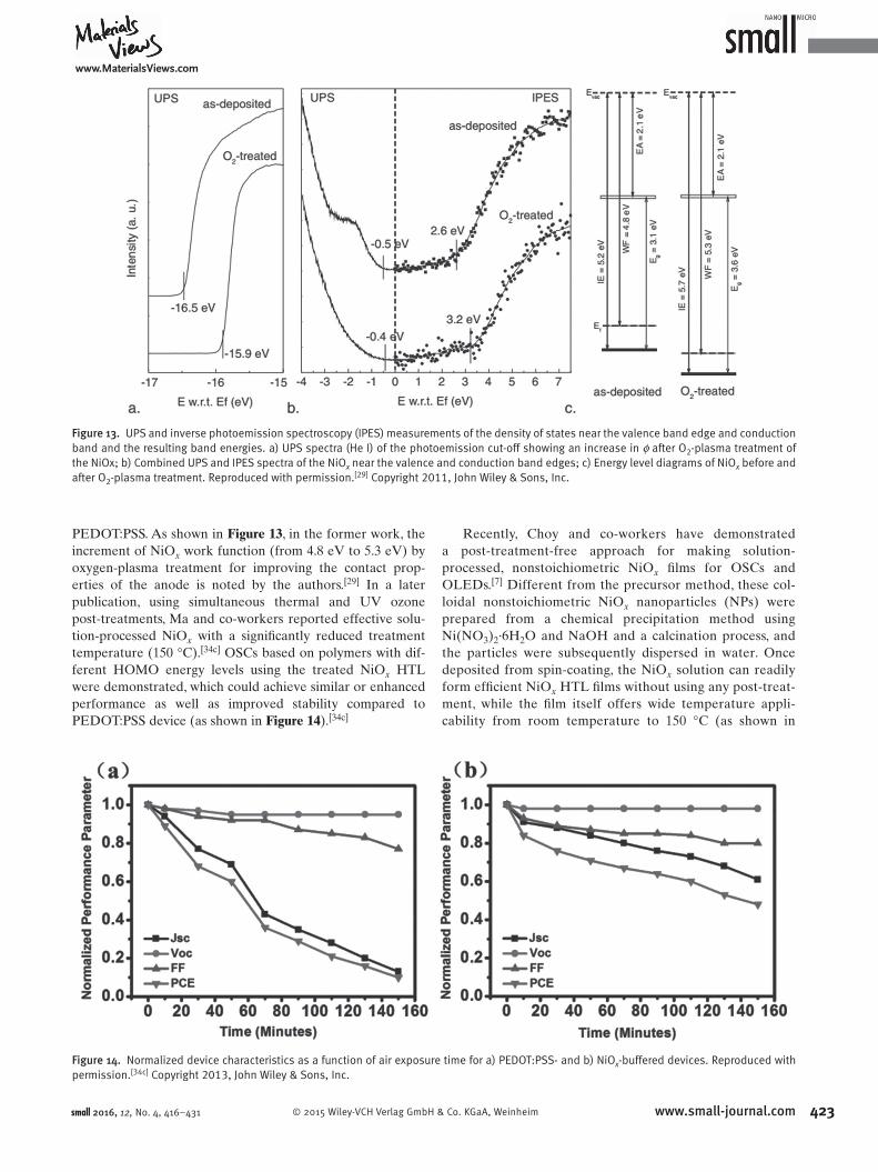
PEDOT:PSS. As shown in Figure 13 , in the former work, the
increment of NiO x work function (from 4.8 eV to 5.3 eV) by
oxygen-plasma treatment for improving the contact prop-
erties of the anode is noted by the authors. [ 29 ] In a later
publication, using simultaneous thermal and UV ozone
post-treatments, Ma and co-workers reported effective solu-
tion-processed NiO x with a signifi cantly reduced treatment
temperature (150 °C). [ 34c ] OSCs based on polymers with dif-
ferent HOMO energy levels using the treated NiO x HTL
were demonstrated, which could achieve similar or enhanced
performance as well as improved stability compared to
PEDOT:PSS device (as shown in Figure 14 ). [ 34c ]
Recently, Choy and co-workers have demonstrated
a post-treatment-free approach for making solution-
processed, nonstoichiometric NiO x fi lms for OSCs and
OLEDs. [ 7 ] Different from the precursor method, these col-
loidal nonstoichiometric NiO x nanoparticles (NPs) were
prepared from a chemical precipitation method using
Ni(NO 3 ) 2 ·6H 2 O and NaOH and a calcination process, and
the particles were subsequently dispersed in water. Once
deposited from spin-coating, the NiO x solution can readily
form effi cient NiO x HTL fi lms without using any post-treat-
ment, while the fi lm itself offers wide temperature appli-
cability from room temperature to 150 °C (as shown in
small 2016, 12, No. 4, 416–431
Figure 13. UPS and inverse photoemission spectroscopy (IPES) measurements of the density of states near the valence band edge and conduction band and the resulting band energies. a) UPS spectra (He I) of the photoemission cut-off showing an increase in φ after O 2 -plasma treatment of the NiOx; b) Combined UPS and IPES spectra of the NiO x near the valence and conduction band edges; c) Energy level diagrams of NiO x before and after O 2 -plasma treatment. Reproduced with permission. [ 29 ] Copyright 2011, John Wiley & Sons, Inc.
Figure 14. Normalized device characteristics as a function of air exposure time for a) PEDOT:PSS- and b) NiO x -buffered devices. Reproduced with permission. [ 34c ] Copyright 2013, John Wiley & Sons, Inc.

reviewswww.MaterialsViews.com
424 www.small-journal.com © 2015 Wiley-VCH Verlag GmbH & Co. KGaA, Weinheim
Table 1 ). [ 7 ] For annealing temperatures above 200 °C, the
WF of NiO x decreased signifi cantly, preventing the NiO x
HTL from effi ciently extracting holes to the electrode due
to the large energy mismatch. An enhanced average PCE
of 9.16% was achieved in OSCs using the NiO x HTL com-
pared to the conventional PEDOT:PSS, and a similar trend
was also observed in OLED devices (as shown in Figure 15
and Figure 16 , respectively). [ 7 ]
3. Solution-Processed Electron Transport Layers
Equally as important as the HTL, the ETL serves as an essen-
tial component in the multilayered organic optoelectronic
device for effi ciently extracting electrons from the cathode.
Among n-type metal oxides, titanium oxide (TiO x ), zinc oxide
(ZnO), and cesium carbonate (Cs 2 CO 3 ) are popular choices
small 2016, 12, No. 4, 416–431
Table 1. Device performance of different annealing temperatures of NiO x -based OSCs with a conventional structure of ITO/NiO x /P3HT:PC 61 BM/Ca/Al. Reproduced with permission. [ 7 ] Copyright 2015, John Wiley & Sons, Inc.
NiO x Annealing Temperature
V OC [V]
J SC [mA cm −2 ]
FF [%]
R S [Ω cm 2 ]
PCE [%]
w/o 0.588 ± 0.001 9.72 ± 0.24 67.31 ± 0.76 2.10 ± 0.07 3.83 ± 0.10
50 °C 0.587 ± 0.003 9.68 ± 0.31 66.16 ± 0.80 2.24 ± 0.10 3.77 ± 0.15
100 °C 0.588 ± 0.002 9.67 ± 0.16 67.20 ± 0.62 2.13 ± 0.04 3.81 ± 0.07
150 °C 0.581 ± 0.004 9.82 ± 0.22 66.50 ± 0.65 2.16 ± 0.07 3.80 ± 0.09
200 °C 0.560 ± 0.004 9.01 ± 0.37 57.90 ± 1.35 4.17 ± 0.11 2.92 ± 0.24
300 °C 0.481 ± 0.008 8.96 ± 0.35 42.99 ± 2.58 7.36 ± 0.09 1.85 ± 0.32
Figure 15. Representative J – V characteristics under AM1.5G solar spectrum for OSCs. The device structures are a) ITO/NiO x or PEDOT:PSS /PCDTBT:PC 71 BM /Ca /Al; b) ITO/NiO x or PEDOT:PSS /PTB7:PC 71 BM /Ca/Al; c) ITO/NiO x or PEDOT:PSS /PTB7-Th:PC 71 BM /Ca/Al; d) IPCE measurements for ITO/NiO x or PEDOT:PSS /PTB7-Th:PC 71 BM /Ca/Al. Reproduced with permission. [ 7 ] Copyright 2015, John Wiley & Sons, Inc.

www.MaterialsViews.com
425© 2015 Wiley-VCH Verlag GmbH & Co. KGaA, Weinheim www.small-journal.com
for solution-processed ETLs for high-performance organic
devices. Recent efforts for further improving the feasibility
and performance of the metal oxide ETLs include developing
low-cost, low-temperature, and large-area solution-processed
approaches which are easily scalable to large-area applica-
tions, and enhancing the optical and electrical properties of
the solution-processed ETLs (including some interesting
optically induced electrical effects) by doping with nanoma-
terials, oxides with different WFs, small molecules, etc., which
will be discussed below.
3.1. Solution-Processed Titanium Oxide (TiO x )
Owing to its low WF, wide bandgap, good electron conduc-
tion, and optical properties, TiO x has been widely adopted
in organic optoelectronics for electron-selective transport
and extraction. Found in many inverted-structure OSCs, tita-
nium oxide (TiO x ) ETLs are mainly categorized into amor-
phous TiO x and anatase/rutile TiO 2 , with different material
properties.
A sol–gel process with a TiO x precursor solution is
one of the commonly used approaches for preparing solu-
tion-based TiO x ETLs in OSCs. The reaction based on
titanium(IV) isopropoxide mainly consists of hydrolysis,
condensation, and stabilization to obtain the precursor
solution. [ 35,36 ] It has been reported that such sol–gel-based
approaches can achieve low-temperature [ 36b ] or even
room-temperature processing without requiring any ini-
tial (UV–ozone or oxygen-plasma) or additional (thermal
annealing or air exposure) treatments before or after the
coating of the TiO x ETL. [ 35 ] As shown in Figure 17 , inverted
small 2016, 12, No. 4, 416–431
Figure 16. Representative a) J – V – L and b) LE–J–L characteristics of OLEDs (triangular markers for PEDOT:PSS device, circular markers for NiO x device). Reproduced with permission. [ 7 ] Copyright 2015, John Wiley & Sons, Inc.
Figure 17. J–V measurements of inverted solar cells based on P3HT:PC60BM and PCDTBT:PC70BM active layers. The active layer was directly spin-cast onto the glass/ITO/TiO x or glass/ITO surfaces at room temperature. Reproduced with permission. [ 35 ] Copyright 2013, Elsevier B.V.

reviewswww.MaterialsViews.com
426 www.small-journal.com © 2015 Wiley-VCH Verlag GmbH & Co. KGaA, Weinheim
OSCs employing the room-temperature solution-pro-
cessed TiO x ETL demonstrated a high PCE of 6.3% in a
PCDTBT:PC 70 BM blend system. [ 35 ]
Alternatively, TiO x ETL fi lms may be formed directly
from anatase TiO x NPs dispersed in an alcohol-based solu-
tion obtained from TiCl 4 via a nonaqueous method. [ 38 ]
Based on this preparation method, Choy and co-workers
demonstrated a facile solution-deposition approach for
forming uniform TiO x ETL fi lm which can be easily scalable
to large area applications. [ 37 ] After a small amount of TiO x
NP solution was cast onto the substrate, a petri dish cover
was used to slow the rate at which the solvent (ethanol)
evaporated, allowing the ETL NPs to align and assemble
instead of aggregating. Thus, large-area, smooth, and uni-
form fi lms could be formed (self-assembled fi lms as large
as 4” × 4” were demonstrated), which showed a different
morphology to fi lms formed by drop-casting ( Figure 18 ). [ 37 ]
Consequently, OSCs made from different locations of the
large-area fi lm (cut into smaller pieces) showed enhanced
PCE compared to spin-coated ETL with small variation, as
shown in Figure 19 . [ 37 ]
To further improve the optical/electrical properties of
solution-processed ETLs for high-performance optoelec-
tronic devices, doping of the ETL solutions with different
types of materials has been studied, with considerable
enhancement observed. Yang and co-workers reported
the doping of cesium carbonate (CsCO 3 ) into a TiO x pre-
cursor. [ 41 ] Besides stabilizing the morphology of the ETL,
the doped cesium TiO x also led to a more desirable WF
for charge extraction in OSCs. As a result, a very high
PCE of 4.2% was reached in P3HT:PC 70 BM-based OSCs
using the Cs-doped TiO x ETL. [ 41 ] Furthermore, doping of
n-type ETLs with metal nanomaterials in OSCs is another
attractive way to further enhance the device performance.
Light soaking is a common occurrence for wide-bandgap
n-type oxides such as TiO x and ZnO, which typically
require high-energy UV exposure before the oxides can
small 2016, 12, No. 4, 416–431
Figure 18. a) Large-area 4” × 4” self-assembled TiO 2 fi lm. The marked regions are extracted and utilized in TiO 2 OSC devices. b) TiO 2 fi lm of the same size fabricated without controlling the solvent evaporation: defects can be found on the fi lm, as indicated by the black arrows. c) Schematic of inverted OSCs with TiO 2 as electron transport layer. Reproduced with permission. [ 37 ] Copyright 2012, Elsevier B.V.
Figure 19. a) J–V characteristics of inverted OSCs with TiO 2 fi lms as electron transport layers by spin-coating and self-assembly (SA) methods, under AM1.5G 100 mW cm −2 illumination. The device performances are summarized in the inset table (including average device performance of large-area SA TiO 2 fi lms. (b) J–V characteristics of electron-only devices with spin-coated and self-assembled TiO 2 fi lms. Reproduced with permission. [ 37 ] Copyright 2012, Elsevier B.V.
Figure 20. Incident photon-to-current conversion effi ciency (IPCE) spectra of pristine TiO 2 and Au NP–TiO 2 composite (TiO 2 +Au NPs) P3HT:PC 61 BM OSCs before and after plasmonic illumination with 600 nm light and an applied voltage bias. All OSCs are measured from the as-fabricated state and the wavelength range of the IPCE measurement is from 450 nm to 800 nm, to avoid the UV region. Reproduced with permission. [ 39 ] Copyright 2013, John Wiley & Sons, Inc.

www.MaterialsViews.com
427© 2015 Wiley-VCH Verlag GmbH & Co. KGaA, Weinheim www.small-journal.comsmall 2016, 12, No. 4, 416–431
be activated and effi ciently conduct electrons. [ 42 ] Due to
the concern that the organic active layer in OSCs may
degrade from long UV exposure, [ 43 ] it is therefore desir-
able to develop metal oxide ETLs which do not need UV
activation. Recently, a novel solution-processed composite
TiO x ETL incorporating Au or Ag NPs was proposed for
high-performance OSCs, reaching a PCE of 8.74%. [ 39,44 ]
Remarkably, by employing plasmonic excitation (at longer
wavelengths of 560–600 nm), charge extraction in the TiO x
ETL could be activated and enhanced by a charge-transfer
process from the NPs to the TiO x , lowering the effec-
tive extraction barrier (as demonstrated by the incident
photon-to-current conversion effi ciency (IPCE) spectra of
OSCs using the composite ETL after 600 nm illumination
shown in Figure 20 ). [ 39 ] The optically induced electrical
effect (termed the plasmonic-electrical
effect) was later confi rmed and further
studied by Riedl and co-workesr (as
shown in Figure 21 ), [ 40 ] although hot
holes were considered to be transferred
during plasmonic illumination. Besides
these plasmonic-electrical effects, elec-
trical enhancement under just UV light
(e.g., under solar illumination) by the
charge accumulation effect of the metal
NPs embedded in the TiO x ETL was
also reported, which gave rise to low-
ered WFs for assisting charge extraction
( Figure 22 ). [ 44 ] The charge accumulation
was evidenced by a blue-shift of the res-
onance frequency of the localized plas-
monic resonance, which confi rmed the
transfer and accumulation of electrons
from TiO x into metal NPs to be the dom-
inant process. [ 44 ]
3.2. Solution-Processed Zinc Oxide (ZnO)
Zinc oxide (ZnO) is another widely used n-type ETL with a
wide bandgap of 3.40 eV [ 45 ] and a low WF of –4.1 eV. [ 46 ] Sim-
ilar to TiO x , solution-processed ZnO ETLs can be prepared
from sol–gel precursors [ 46,47 ] or ZnO NP solutions. [ 48 ]
Using zinc acetate dehydrate as precursor in 2-methox-
yethanol and thermal annealing, Heeger and co-workers
reported inverted OSCs with low-temperature solution pro-
cessed ZnO ETL, yielding a high average effi ciency of 6.08%
at an annealing temperature of 200 °C ( Figure 23 ). [ 47c ] Inter-
estingly, the inverted OSCs with ZnO ETLs were air-stable,
retaining ≈80% PCE after a month (Figure 23 ). [ 47c ] Similarly,
the ZnO ETLs prepared from ZnO NP solutions reported
by Jen and co-workers demonstrated excellent stability in
inverted, fl exible OSC devices in air as well, with superior
lifetimes of >40 days for unencapsulated cells compared to
normal-structure devices ( Figure 24 ). [ 48a ] Besides increasing
device stability, ZnO has also been shown to offer optical
enhancement by fulfi lling the role of an optical spacer for
improving photocarrier generation. [ 47d ]
Through the combinational plasmonic effects of a metal
grating and metal NPs (doped into ZnO ETLs), broad-
band absorption enhancements in the range of 350–800 nm
due to multiple plasmonic effects in a single OSC device
was observed. [ 50 ] Recently, a novel design doping the light
absorber perylene bisimide (PBI-H) into a sol–gel ZnO
ETL to enhance its photoconductivity was reported. [ 49 ]
Simultaneous enhancements in short-circuit current den-
sity ( J SC ), V OC , and FF were observed in OSCs using doped
ZnO ETLs compared to devices using neat ZnO, as shown
in Figure 25 . [ 49 ] As a result, a very high PCE of 10.5% was
achieved in PTB7-Th-based OSCs, which is one of the highest
PCEs for single-junction cells. Interestingly, owing to the high
conductivity of the doped ETL, the performance of OSCs
remained stable over a wide range of ZnO thicknesses (from
30 to 60 nm), as shown in Figure 26 . [ 49 ]
Figure 21. a) Layer sequence of inverted OSCs with a plasmonically sensitized cathode interlayer, and b) J/V characteristics of a corresponding PCDTBT/ PC 70 BM-based OSC under AM1.5 illumination with a UV blocking fi lter (λ > 400 nm). The characteristics of an OSC with a neat TiO x interlayer (w/o Ag NP) are shown as a reference. Reproduced with permission. [ 40 ] Copyright 2015, Macmillan Publishers Limited.
Figure 22. Diagram of WF changes of the TiO 2 fi lm, Au NP–TiO 2 fi lm, and Ag NP–TiO 2 fi lm from dark conditions to UV illumination (for 15 min), as measured by a Kelvin probe. Reproduced with permission. [ 44 ] Copyright 2013, Royal Society of Chemistry.

reviewswww.MaterialsViews.com
428 www.small-journal.com © 2015 Wiley-VCH Verlag GmbH & Co. KGaA, Weinheim small 2016, 12, No. 4, 416–431
3.3. Solution-Processed Cesium Carbonate (Cs 2 CO 3 )
Cesium carbonate (Cs 2 CO 3 ) is another promising candidate
for solution-processed ETLs which has been extensively
employed in OLEDs and OSCs, due to its good electron-
injecting capability. [ 51 ] Solution-processed Cs 2 CO 3 ETLs can
be prepared directly by spin-coating Cs 2 CO 3 in aqueous, [ 52 ]
2-methoxyethanol, [ 51a ] or 2-ethoxyethanol solutions. [ 53 ]
Yang and co-workers reported highly effi cient inverted
OSCs using solution-processed Cs 2 CO 3 dissolved in
2-ethoxyethanol. [ 53c ] Upon thermal annealing, Cs 2 CO 3
decomposed into the doped oxide of Cs 2 O with a low WF,
which was responsible for the improvement in device per-
formance. An inverted OSCs using a Cs 2 CO 3 ETL with
150 °C annealing reached a high PCE of 4.2%, as shown in
Figure 27 . [ 53c ]
Recently, Liao and co-workers demonstrated an adjust-
able WF of an aqueous, solution-processed Cs 2 CO 3 ETL by
doping MoO 3 or Na 2 WO 4 . [ 52 ] Continuous WF tuning with a
large variation range was achieved, as shown in Figure 28 .
The lowering of the effective WF led to the improvement of
V OC in P3HT:ICBA OSCs, yielding a high PCE of 5.25% by
Na 2 WO 4 -doped Cs 2 CO 3 . Accordingly, the authors concluded
that the decreased WF of the doped ETL was from the gen-
erated Mo–O–Cs and/or W–O–Cs composites. [ 52 ]
4. Conclusion
With the promise of being low-cost, light-weight, mechanically
fl exible, and highly effi cient, organic optoelectronic devices
such as OSCs and OLEDs have spurred extensive interest
aiming for practical applications within the near future.
The development of organic optoelectronics has, however,
reached a pivotal stage, with the PCE of single-junction OSCs
surpassing the 10% threshold. Due to concerns over the sta-
bility (e.g., air or temperature sensitivity) and fabrication costs
(e.g., high vacuum or thermal deposition) of conventional
materials, solution-processed metal oxide CTLs (both ETLs
and HTLs) are an important step towards achieving low-cost,
stable, and fl exible organic devices. Here, we have reviewed
the recent progress in solution-processed metal oxide CTLs
in organic optoelectronic devices. Signifi cant advances in
metal oxide CTLs have enabled low- or even room-temper-
ature processing for many types of metal oxides, which is
essential for improving the processability and scalability for
mass and large-area production. Besides further improving
Figure 23. a) J–V characteristics of inverted PCDTBT:PC 70 BM solar cells incorporating ZnO fi lms with the indicated annealing temperatures. b) IPCE spectra of inverted PCDTBT:PC 70 BM solar cells. c) Dark current of inverted PCDTBT:PC 70 BM solar cells. d) Normalized PCEs for inverted PCDTBT:PC 70 BM solar cells as a function of storage time in air under ambient conditions. Reproduced with permission. [ 47c ] Copyright 2011, John Wiley & Sons, Inc.

www.MaterialsViews.com
429© 2015 Wiley-VCH Verlag GmbH & Co. KGaA, Weinheim www.small-journal.com
the feasibility and quality of the synthesized metal oxides,
the doping of metal oxide CTLs has recently been demon-
strated as an effi cient tool for the enhancement of device per-
formance. Furthermore, other low-cost OSC materials, such
as non-fullerene material systems promising lowered costs
from replacing the fullerene and higher output voltage, [ 54 ]
are attractive platforms for further incorporating solution-
processed metal oxide CTLs for the future development of
affordable and high-performance OSCs. Besides the pop-
ular choice of oxide materials reviewed here, other types of
metal oxides may also be considered for solution processing
for versatile energy alignment and diverse applications, such
as chromium oxide, [ 55 ] iridium oxide, [ 56 ] and rhenium oxide;
solution-processed rhenium oxide was recently reported. [ 57 ]
To overcome the current limitations to the optical, electrical,
chemical, and mechanical properties of metal oxide CTLs,
further research efforts are required in this fi eld to improve
the performance of the OSCs and OLEDs.
small 2016, 12, No. 4, 416–431
Figure 24. a) J–V characteristics of unencapsulated, conventional P3HT:PCBM bulk-heterojunction solar cells over a period of four days in air under ambient conditions. b) J–V characteristics of unencapsulated inverted P3HT:PCBM bulk-heterojunction solar cells (ZnO NPs on an ITO-coated plastic substrate) over a period of 40 days in air under ambient conditions. Inset: unencapsulated dark current device characteristics at 0 and 40 days in air under ambient conditions. Reproduced with permission. [ 48a ] Copyright 2008, AIP Publishing LLC.
Figure 25. a) J−V characteristics of the OSCs under 1000 W m −2 AM1.5G illumination. b) EQE curves. Device confi gurations are ITO/ZnO (30 nm) or ZnO:PBI-H (30 nm)/PTB7:PC 71 BM (100 nm)/MoO 3 (10 nm)/Al (100 nm). Reproduced with permission. [ 49 ] Copyright 2015, American Chemical Society.
Figure 26. Effects of the thickness of the ZnO:PBI-H cathode interlayer on device performance. Device confi guration: ITO/ZnO:PBI-H (30–60 nm)/PTB7 or PTB7-Th:PC 71 BM (100 nm)/MoO 3 (10 nm)/Al (100 nm). Average values of seven cells with standard deviation. Reproduced with permission. [ 49 ] Copyright 2015, American Chemical Society.

reviewswww.MaterialsViews.com
430 www.small-journal.com © 2015 Wiley-VCH Verlag GmbH & Co. KGaA, Weinheim
Acknowledgements
This work was supported by the General Research Fund (grants: HKU711612E), the Collaborative Research Fund (grant CUHK1/CRF/12G and grant C7045–14E), and the RGC-NSFC grant (N_HKU709/12) from the Research Grants Council of Hong Kong Spe-cial Administrative Region, China as well as grant CAS14601 from the CAS-Croucher Funding Scheme for Joint Laboratories from the Croucher Foundation. The authors acknowledge the help of Jian Mao for preparing the manuscript.
[1] a) S. Chen , J. R. Manders , S.-W. Tsang , F. So , J. Mater. Chem. 2012 , 22 , 24202 ; b) M. T. Greiner , Z.-H. Lu , NPG Asia Mater. 2013 , 5 , e55 .
[2] M. T. Greiner , L. Chai , M. G. Helander , W.-M. Tang , Z.-H. Lu , Adv. Funct. Mater. 2012 , 22 , 4557 .
[3] S. Tokito , K. Noda , Y. Taga , J. Phys. D: Appl. Phys. 1996 , 29 , 2750 . [4] H. Tang , F. Li , J. Shinar , Appl. Phys. Lett. 1997 , 71 , 2560 . [5] M. T. Greiner , M. G. Helander , W.-M. Tang , Z.-B. Wang , J. Qiu ,
Z.-H. Lu , Nat. Mater. 2012 , 11 , 76 . [6] K. Zilberberg , J. Meyer , T. Riedl , J. Mater. Chem. C 2013 , 1 , 4796 . [7] F. Jiang , W. C. Choy , X. Li , D. Zhang , J. Cheng , Adv. Mater. 2015 ,
27 , 2930 . [8] M. Kroger , S. Hamwi , J. Meyer , T. Riedl , W. Kowalsky , A. Kahn ,
Appl. Phys. Lett. 2009 , 95 , 123301 . [9] V. Shrotriya , G. Li , Y. Yao , C.-W. Chu , Y. Yang , Appl. Phys. Lett.
2006 , 88 , 073508 . [10] a) S.-Y. Lin , C.-M. Wang , K.-S. Kao , Y.-C. Chen , C.-C. Liu , J. Sol-Gel
Sci. Technol. 2010 , 53 , 51 ; b) C. Girotto , E. Voroshazi , D. Cheyns , P. Heremans , B. P. Rand , ACS Appl. Mater. Interfaces 2011 , 3 , 3244 ; c) T. Yang , M. Wang , Y. Cao , F. Huang , L. Huang , J. Peng , X. Gong , S. Z. Cheng , Y. Cao , Adv. Energy Mater. 2012 , 2 , 523 .
[11] a) F. Liu , S. Shao , X. Guo , Y. Zhao , Z. Xie , Sol. Energy Mater. Sol. Cells 2010 , 94 , 842 ; b) S. R. Hammond , J. Meyer , N. E. Widjonarko , P. F. Ndione , A. K. Sigdel , A. Garcia , A. Miedaner , M. T. Lloyd , A. Kahn , D. S. Ginley , J. Mater. Chem. 2012 , 22 , 3249 .
[12] a) J. J. Jasieniak , J. Seifter , J. Jo , T. Mates , A. J. Heeger , Adv. Funct. Mater. 2012 , 22 , 2594 ; b) Z. Tan , D. Qian , W. Zhang , L. Li , Y. Ding , Q. Xu , F. Wang , Y. Li , J. Mater. Chem. A 2013 , 1 , 657 ; c) K. Zilberberg , H. Gharbi , A. Behrendt , S. Trost , T. Riedl , ACS Appl. Mater. Interfaces 2012 , 4 , 1164 .
[13] J. Meyer , R. Khalandovsky , P. Görrn , A. Kahn , Adv. Mater. 2011 , 23 , 70 .
[14] F. Xie , W. C. Choy , C. Wang , X. Li , S. Zhang , J. Hou , Adv. Mater. 2013 , 25 , 2051 .
[15] A. Soultati , A. M. Douvas , D. G. Georgiadou , L. C. Palilis , T. Bein , J. M. Feckl , S. Gardelis , M. Fakis , S. Kennou , P. Falaras , T. Stergiopoulos , N. A. Stathopoulos , D. Davazoglou , P. Argitis , M. Vasilopoulou , Adv. Energy Mater. 2014 , DOI: 10.1002/aenm.201300896 .
[16] X. Li , W. C. Choy , F. Xie , S. Zhang , J. Hou , J. Mater. Chem. A 2013 , 1 , 6614 .
[17] a) J.-S. Huang , C.-Y. Chou , M.-Y. Liu , K.-H. Tsai , W.-H. Lin , C.-F. Lin , Org. Electron. 2009 , 10 , 1060 ; b) J.-H. Huang , T.-Y. Huang , H.-Y. Wei , K.-C. Ho , C.-W. Chu , RSC Adv. 2012 , 2 , 7487 .
[18] K. Zilberberg , S. Trost , H. Schmidt , T. Riedl , Adv. Energy Mater. 2011 , 1 , 377 .
[19] K. Zilberberg , S. Trost , J. Meyer , A. Kahn , A. Behrendt , D. Lützenkirchen-Hecht , R. Frahm , T. Riedl , Adv. Funct. Mater. 2011 , 21 , 4776 .
[20] Y. Tan , W. Zhang , C. Cui , Y. Ding , D. Qian , Q. Xu , L. Li , S. Li , Y. Li , Phys. Chem. Chem. Phys. 2012 , 14 , 14589 .
[21] X. Li , F. Xie , S. Zhang , J. Hou , W.-C. Choy , Light: Sci. Appl. 2015 , 4 , e273 . [22] X. Li , F. Xie , S. Zhang , J. Hou , W. C. Choy , Adv. Funct. Mater. 2014 ,
24 , 7348 . [23] J.-S. Huang , C.-Y. Chou , C.-F. Lin , IEEE Electron Device Lett. 2010 ,
31 , 332 . [24] a) N. Li , T. Stubhan , N. A. Luechinger , S. C. Halim , G. J. Matt ,
T. Ameri , C. J. Brabec , Org. Electron. 2012 , 13 , 2479 ; b) T. Stubhan , N. Li , N. A. Luechinger , S. C. Halim , G. J. Matt , C. J. Brabec , Adv. Energy Mater. 2012 , 2 , 1433 .
[25] H. Choi , B. Kim , M. J. Ko , D.-K. Lee , H. Kim , S. H. Kim , K. Kim , Org. Electron. 2012 , 13 , 959 .
[26] N. Özer , Thin Solid Films 1997 , 304 , 310 . [27] Z. a. Tan , L. Li , C. Cui , Y. Ding , Q. Xu , S. Li , D. Qian , Y. Li , J. Phys.
Chem. C 2012 , 116 , 18626 . [28] W. C. H. Choy , F. Xie , C. D. Wang , PCT/CN2013/082830 , 2013 . [29] K. X. Steirer , P. F. Ndione , N. E. Widjonarko , M. T. Lloyd , J. Meyer ,
E. L. Ratcliff , A. Kahn , N. R. Armstrong , C. J. Curtis , D. S. Ginley , J. J. Berry , D. C. Olson , Adv. Energy Mater. 2011 , 1 , 813 .
[30] a) Z. Huang , G. Natu , Z. Ji , M. He , M. Yu , Y. Wu , J. Phys. Chem. C 2012 , 116 , 26239 ; b) A. Garcia , G. C. Welch , E. L. Ratcliff , D. S. Ginley , G. C. Bazan , D. C. Olson , Adv. Mater. 2012 , 24 , 5368 .
small 2016, 12, No. 4, 416–431
Figure 27. I–V characteristics of the inverted OSC devices under illumination with various annealing temperatures of the Cs 2 CO 3 layer. Reproduced with permission. [ 53c ] Copyright 2008, AIP Publishing LLC.
Figure 28. The effective WF and V OC of different concentrations of Cs 2 CO 3 with and without doping MoO 3 or Na 2 WO 4 . Reproduced with permission. [ 52 ] Copyright 2014, Royal Society of Chemistry.

www.MaterialsViews.com
431© 2015 Wiley-VCH Verlag GmbH & Co. KGaA, Weinheim www.small-journal.com
[31] M. D. Irwin , D. B. Buchholz , A. W. Hains , R. P. Chang , T. J. Marks , Proc. Natl. Acad. Sci. 2008 , 105 , 2783 .
[32] W. Yu , L. Shen , S. Ruan , F. Meng , J. Wang , E. Zhang , W. Chen , Sol. Energy Mater. Sol. Cells 2012 , 98 , 212 .
[33] S.-Y. Park , H.-R. Kim , Y.-J. Kang , D.-H. Kim , J.-W. Kang , Sol. Energy Mater. Sol. Cells 2010 , 94 , 2332 .
[34] a) K. H. Kim , C. Takahashi , T. Okubo , Y. Abe , M. Kawamura , Appl. Surf. Sci. 2012 , 258 , 7809 ; b) S. Bai , M. Cao , Y. Jin , X. Dai , X. Liang , Z. Ye , M. Li , J. Cheng , X. Xiao , Z. Wu , Z. Xia , B. Sun , E. Wang , Y. Mo , F. Gao , F. Zhang , Adv. Energy Mater. 2014 , DOI: 10.1002/aenm.201301460 ; c) Z. Zhai , X. Huang , M. Xu , J. Yuan , J. Peng , W. Ma , Adv. Energy Mater. 2013 , 3 , 1614 ; d) J. R. Manders , S. W. Tsang , M. J. Hartel , T. H. Lai , S. Chen , C. M. Amb , J. R. Reynolds , F. So , Adv. Funct. Mater. 2013 , 23 , 2993 ; e) X. Fan , G. Fang , F. Cheng , P. Qin , H. Huang , Y. Li , J. Phys. D: Appl. Phys. 2013 , 46 , 305106 .
[35] A. Hadipour , R. Müller , P. Heremans , Org. Electron. 2013 , 14 , 2379 .
[36] a) L. Sun , W. Shen , W. Chen , X. Bao , N. Wang , X. Dou , L. Han , S. Wen , Thin Solid Films 2014 , 573 , 134 ; b) K. H. Wong , C. W. Mason , S. Devaraj , J. Ouyang , P. Balaya , ACS Appl. Mater. Interfaces 2014 , 6 , 2679 ; c) J. Y. Kim , S. H. Kim , H. H. Lee , K. Lee , W. Ma , X. Gong , A. J. Heeger , Adv. Mater. 2006 , 18 , 572 .
[37] D. Zhang , W. C. H. Choy , F.-x. Xie , X. Li , Org. Electron. 2012 , 13 , 2042 .
[38] a) G. V. Jensen , M. Bremholm , N. Lock , G. R. Deen , T. R. Jensen , B. B. Iversen , M. Niederberger , J. S. Pedersen , H. Birkedal , Chem. Mater. 2010 , 22 , 6044 ; b) H. L. Zhu , W. C. Choy , W. E. Sha , X. Ren , Adv. Optical Mater. 2014 , 2 , 1082 .
[39] D. Zhang , W. C. H. Choy , F. Xie , W. E. I. Sha , X. Li , B. Ding , K. Zhang , F. Huang , Y. Cao , Adv. Funct. Mater. 2013 , 23 , 4255 .
[40] S. Trost , T. Becker , K. Zilberberg , A. Behrendt , A. Polywka , R. Heiderhoff , P. Görrn , T. Riedl , Sci. Rep. 2015 , 5 , 7765 .
[41] M.-H. Park , J.-H. Li , A. Kumar , G. Li , Y. Yang , Adv. Funct. Mater. 2009 , 19 , 1241 .
[42] S. Trost , K. Zilberberg , A. Behrendt , A. Polywka , P. Görrn , P. Reckers , J. Maibach , T. Mayer , T. Riedl , Adv. Energy Mater. 2013 , 3 , 1437 .
[43] S. Chambon , A. Rivaton , J.-L. Gardette , M. Firon , Sol. Energy Mater. Sol. Cells 2007 , 91 , 394 .
[44] F. Xie , W. C. H. Choy , W. E. I. Sha , D. Zhang , S. Q. Zhang , X. C. Li , C. W. Leung , J. H. Hou , Energy Environ. Sci. 2013 , 6 , 3372 .
[45] B. E. Sernelius , K.-F. Berggren , Z.-C. Jin , I. Hamberg , C. Granqvist , Phys. Rev. B 1988 , 37 , 10244 .
[46] M. White , D. Olson , S. Shaheen , N. Kopidakis , D. S. Ginley , Appl. Phys. Lett. 2006 , 89 , 143517 .
[47] a) Y.-J. Kang , K. Lim , S. Jung , D.-G. Kim , J.-K. Kim , C.-S. Kim , S. H. Kim , J.-W. Kang , Sol. Energy Mater. Sol. Cells 2012 , 96 , 137 ; b) Z. Ma , Z. Tang , E. Wang , M. R. Andersson , O. Inganä s , F. Zhang , J. Phys. Chem. C 2012 , 116 , 24462 ; c) Y. Sun , J. H. Seo , C. J. Takacs , J. Seifter , A. J. Heeger , Adv. Mater. 2011 , 23 , 1679 ; d) A. K. K. Kyaw , D. H. Wang , D. Wynands , J. Zhang , T.-Q. Nguyen , G. C. Bazan , A. J. Heeger , Nano Lett. 2013 , 13 , 3796 .
[48] a) S. K. Hau , H.-L. Yip , N. S. Baek , J. Zou , K. O’Malley , A. K. Y. Jen , Appl. Phys. Lett. 2008 , 92 , 253301 ; b) S. Alem , J. Lu , R. Movileanu , T. Kololuoma , A. Dadvand , Y. Tao , Org. Electron. 2014 , 15 , 1035 ; c) F. C. Krebs , S. A. Gevorgyan , J. Alstrup , J. Mater. Chem. 2009 , 19 , 5442 .
[49] L. Nian , W. Zhang , N. Zhu , L. Liu , Z. Xie , H. Wu , F. Würthner , Y. Ma , J. Am. Chem. Soc. 2015 , 137 , 6995 .
[50] X. Li , X. Ren , F. Xie , Y. Zhang , T. Xu , B. Wei , W. C. H. Choy , Adv. Optical Mater. 2015 , DOI: 10.1002/adom.201500107 .
[51] a) L. P. Lu , D. Kabra , K. Johnson , R. H. Friend , Adv. Funct. Mater. 2012 , 22 , 144 ; b) G. Li , C. Chu , V. Shrotriya , J. Huang , Y. Yang , Appl. Phys. Lett. 2006 , 88 , 253503 .
[52] M.-F. Xu , Y.-J. Liao , F.-S. Zu , J. Liang , D.-X. Yuan , Z.-K. Wang , L.-S. Liao , J. Mater. Chem. A 2014 , 2 , 9400 .
[53] a) G. Cheng , W.-Y. Tong , K.-H. Low , C.-M. Che , Sol. Energy Mater. Sol. Cells 2012 , 103 , 164 ; b) Y.-I. Lee , J.-H. Youn , M.-S. Ryu , J. Kim , H.-T. Moon , J. Jang , Org. Electron. 2011 , 12 , 353 ; c) H.-H. Liao , L.-M. Chen , Z. Xu , G. Li , Y. Yang , Appl. Phys. Lett. 2008 , 92 , 173303 .
[54] a) E. Zhou , J. Cong , Q. Wei , K. Tajima , C. Yang , K. Hashimoto , Angew. Chem., Int. Ed. 2011 , 50 , 2799 ; b) E. Zhou , J. Cong , M. Zhao , L. Zhang , K. Hashimoto , K. Tajima , Chem. Commun. 2012 , 48 , 5283 ; c) E. Zhou , J. Cong , K. Hashimoto , K. Tajima , Adv. Mater. 2013 , 25 , 6991 ; d) E. Zhou , M. Nakano , S. Izawa , J. Cong , I. Osaka , K. Takimiya , K. Tajima , ACS Macro Lett. 2014 , 3 , 872 ; e) Y. Geng , J. Huang , K. Tajima , Q. Zeng , E. Zhou , Polymer 2015 , 63 , 164 ; f) X. Wang , J. Huang , K. Tajima , B. Xiao , E. Zhou , Mater. Today Commun. 2015 , 4 , 16 .
[55] P. Qin , G. Fang , Q. He , N. Sun , X. Fan , Q. Zheng , F. Chen , J. Wan , X. Zhao , Sol. Energy Mater. Sol. Cells 2011 , 95 , 1005 .
[56] G. H. Jung , K.-G. Lim , T.-W. Lee , J.-L. Lee , Sol. Energy Mater. Sol. Cells 2011 , 95 , 1146 .
[57] Z. A. Tan , L. Li , F. Wang , Q. Xu , S. Li , G. Sun , X. Tu , X. Hou , J. Hou , Y. Li , Adv. Energy Mater. 2014 , 4 , 1300884 .
Received: July 29, 2015 Revised: September 22, 2015Published online: December 12, 2015
small 2016, 12, No. 4, 416–431