Chapter 8 Amplifiers: Stability, Noise and Gain IF amplifiers
date post
22-Dec-2015Category
view
214download
1
Slide 1
V. PaidiDepartment of Electrical and Computer Engineering,
University of California, Santa Barbara
High Frequency Power Amplifiers

Slide 2
Outline• Research to date
• Class B Power amplifiers in GaN HEMT technology for applications in X-band.
• Design of G-band (140-220 GHz) Power Amplifiers in InP mesa DHBT technology.
• Proposed Future Research
• Fabrication and measurement of G-band ( 140-220 GHz) Power amplifiers in InP DHBT technology
• Process improvements for better yield and performance.

Slide 3
Class B Power amplifiers in GaN HEMT technology
• Push-Pull Vs Single-ended topology.
• Common Source Class B.
• Common Drain Class B.

Slide 4
Why Class B? and Why GaN HEMTs?• Why Class B ?
– Class A: Ideal PAE 50%, feasible PAE 20-30%. However , good linearity.
– Switch mode Amplifiers: Ideal PAE 100%, feasible PAE 60-70 %. Poor Linearity.
– Class B: Ideal PAE 78.6%; feasible PAE 40-50% (typical GaN HEMT at X-band). Potential Low distortion Operation.
• Why GaN HEMTs ?
– Excellent Power density, as high as 12 W/mm in X-band.
– ft ~ 50 GHz and fmax ~ 80 GHz for Lg ~ 0.25m due to high saturation velocity.
– ‘Near Linear’ Id-Vgs Characteristics about threshold leading to a potential low distortion Class B operation.

Slide 5
• Half sinusoidal drain current on each device, but full sinusoidal drain voltage. • Even harmonics are suppressed by symmetry => wide bandwidth (limited by the power combiner). • To obtain high efficiency (78%), a half-sinusoidal current is needed at each drain. This requires an even-harmonic short. This can be achieved at HF/VHF frequencies with transformers or bandpass filters. However,
1. Most wideband microwave baluns can not provide effective broadband short for even-mode. Efficiency is then poor.
2. They occupy a lot of expensive die area on MMIC.
UCSBPush-pull Class BV. Paidi, S. Xie
RL
VG
Vin
Cbias
Cbias
VD
1:1
1:1
Vin-
Vin+
ID+
ID-
Vout
VDS+
VDS-

Slide 6
Push-pull Class B
Single-ended Class B with an output filter
Even harmonics suppressed by symmetry
Even harmonics suppressed by filter
UCSBSingle-ended Class B = push-pull
Bandwidth restriction < 2:1
V. Paidi, S. Xie
Id1Id1
Vin
Id2
Vin Vin
Id
Actual Tranfer Function Even-order components Odd-order components
Id
Vin
Id
Vin Vin
Id
.....33
221 ininincd VIVIVII .....3
32
21 ininincd VIVIVII ..22 331 inin VIVI
.....33
221 ininincd VIVIVII .....2
2 incd VII .....331 inin VIVI
Only harmonic distortion
harmonic + IMD distortion

Slide 7
UCSBLinearity Analysis-Id vs Vgs V. Paidi, S. Xie
.........*** 33
2210 gsgsgs VIVIVIII
0
0.1
0.2
0.3
0.4
0.5
0.6
0.7
0.8
-5 -4 -3 -2 -1 0
Experimental (A/mm)Modeled (A/mm)
Dra
in C
urr
en
t (A
/mm
)
Gate Bias (V)
Near linear characteristics of GaN HEMTs on SiC
The third order term is small about the threshold Voltage
Odd-part creates distortion

Slide 8
UCSBLinearity Analysis-Id vs Vgs Contd.V. Paidi, S. Xie
Ideal Class B Bias too low:Class C
Bias too high:Class AB
Id2
Id
Id
Vin
Vin
Vin
Id Id
Id2Id2
IdId
Vin Vin
Vin Vin
VinVin
Class B bias has the minimum distortion

Slide 9
RF Performance at Vds=15V, Vgs=-3.5V of 0.25X150m2 device
Process and Device Performance
• Lg ~ 0.25um,Idss ~ 1A/mm
• ft ~ 55 GHz (~ 50 GHz for dual gate)
• Vbr ~ 40V (~ 55V for dual gate)
Pulsed IV Curve(80sec) 600m Single gate GaN HEMT
~1.2 A
0
5
10
15
20
25
30
35
40
1 10 100
Sh
ort
Circ
uit
Cu
rre
nt G
ain
(h21
), d
B
frequency, GHz (log scale)
fT = 50GHz
Good Passivation,600mA at Vgs=0V fT~50 GHz
SiC substrate ~400 um
1.4 um GaN buffer
25 nm Al0.3Ga0.7N barrier
60nm AlN Nucleation layer
1nm AlN layer
400 nm Silicon Nitride
Plated Airbridge
Silicon Nitride Passivation Layer
Ti/ Al/ Ni/ Au ohmic Contact
Ni/Au Schottky Contact
UCSBV. Paidi, S. Xie

Slide 10
UCSB
RLTLIN
R1 L1
L2
C1
RF IN
Vg
Vd
BIASTEE Input
matchingnetwork
Outputmatchingnetwork
Cds BIASTEE
(short at 2fo, 3fo...)
Gate 2
Gate 1
Single-ended Class B Power AmplifierS. Xie, V. Paidi
Lossy input matching - section lowpass filter

Slide 11
Class B bias @Vgs = - 5.1V
Single tone performance @ f0 = 8GHz:
Two tone performance @ f1=8GHz, f2=8.001GHz :
15
20
25
30
35
40
0
0.1
0.2
0.3
0.4
0.5
0 5 10 15 20 25 30
Ou
tpu
t po
wer,
db
m
PA
E
Input power, dbm
-50
-40
-30
-20
-10
0
10
20
30
0
0.05
0.1
0.15
0.2
0.25
-15 -10 -5 0 5 10 15 20
Out
put
pow
er,
dBm
PA
E
Input power, dBm
f1,f2
2f1-f2, 2f2-f1
Gain ~ 13 dB,PAE (maximum) ~ 34%
Saturated output power 36 dBm
Good IM3 performance: • 40dBc at Pin = 15 dBm, and• > 35 dBc for Pin < 17.5 dBm
V. Paidi, S. XieUCSB

Slide 12
Summary of IM3 suppression
10
20
30
40
50
60
0 5 10 15 20 25 30 35
IM3 c
om
pre
ssio
n,
dB
c
Pout, dBm
Class BClass A
Class C
Class ABPsat
• Low output power levels (Pout < 24 dBm), Class A and Class B both exhibit good linearity (Class B > 36 dBc, Class A > 45 dBc).
• Higher output power levels, Class A behaves almost the same as Class B.
• Class AB and C exhibit more distortion compared to Class A and B.
V. Paidi, S. XieUCSB

Slide 13
Why Common Drain Class B ?
RL
vi vout
bandpass filter @fo
InputMatchingnetwork
Vdd
Vin Vout
V. Paidi, S. XieUCSB
)( gsmLoadin
out VgRV
VGain
)(1
)(
gsmLoad
gsmLoad
in
out
VgR
VgR
V
VGain
Gain of the Common Drain Class B
Gain of the Common Source Class B
In Common drain design the nonlinearity in gm is suppressed by the feedback term in the denominator.If , then voltage Gain is independent of gm
1)( gs
Vm
gLoad
R
Circuit Schematic
Disadvantage : Maximum stable gain is less for common drain configuration resulting in reduction in efficiency With higher fmax MSG could be better.

Slide 14
Comparison between Common Drain and Common source designs
.15~)36log(10)1log(10
56
30~*
2*
*
dBRgfactorLinearity
V
VV
I
VV
V
IRgfactorFeedback
Loadm
p
kbr
dss
kbr
P
dssLoadm
V. Paidi, S. XieUCSB
0
10
20
30
40
50
60
70
5 10 15 20 25 30 35
IM3
Sup
pre
ssio
n, d
Bc
pout, dBm
12 dB
Common Drain
Common Source
•Common drain and common source designs are @ 10GHz
• Both have 36 dBm of saturated output power.1.2 mm GaN HEMTs are used.
•Common drain design has ~12 dB superior IM3 suppression over the equivalent Common Source design.
• At 1W total output power Common drain exhibits 46 dBc IMD3 Common source exhibits 36 dBc IMD3.

Slide 15
Common Drain Class B Power Amplifier
10
15
20
25
30
35
40
0
0.1
0.2
0.3
0.4
0.5
5 10 15 20 25 30 35
Ou
tpu
t P
ower
, dB
m
PA
E
input power, dbm
0
10
20
30
40
50
60
10 15 20 25 30 35
IM3
Su
ppre
ssio
n,
dBc
Total output power, dBm
V. Paidi, S. XieUCSB
Specifications
• 37 dBm saturated output power at 5 GHz• 8 dB Class B gain, 4-6 GHz bandwidth.• 38% maximum PAE• 44 dBc at 1W total output power under Class B bias.•Being fabricated by Shouxuan Xie
Layout ~6 mm X 2.5mm
Psat ~ 37 dbm
PAE ~ 38 %
IMD3 > 42 dBc for Pout <2 W

Slide 16
Power Amplifiers in InP mesa DHBT technology
• Motivation.
• Layer Structure and process ( Mattias, Zach ).
• Performance of InP mesa DHBT technology ( Mattias, Zach).
• G-band ( 140-220 GHz) Power amplifier design and layout.

Slide 17
Motivation for 140- 220 GHz power amplifiers and Previous results
• Applications for electronics in 140-220 GHz frequency band
Wideband communication systems Atmospheric sensing Automotive radar
• Small signal amplifier results
6.3 dB @ 175 GHz single stage amplifier in InP TSHBT technology, Miguel et.al.,12 dB @ 170 GHz three stage CE amplifier in InP TSHBT technology, Miguel et.
al., 3-stage amplifier with 12-15 dB gain from 160-190 GHz, InP HEMT, Lai et. al. 6-stage amplifier with 20 6 dB from 150-215 GHz, InP HEMT, Weinreb et. al.
• Power amplifier results 12.5 dBm @90 GHz with 8.6 dB gain in TS InP DHBT technology, Yun et. al., 14-16 dBm @140-170 GHz with 10 dB gain in InP HEMT technology, Lorene et. al., 14-16 dBm @65-145 GHz with > 10 dB gain in InP HEMT technology, Lorene et. al.,

Slide 18
Why mesa -InP HBTs for 140- 220 GHz power amplifiers ?
• fmax > 400 GHz for 2100A Collector, 300A base HBT( Technologies like SiGe have fmax ~ 210 GHz Jae- Sung Rieh et al., IBM ( IPRM 2003) )
• High bandwidth as ft > 250 GHz for 2100A Collector, 300A base HBT
• Current density > 3 mA/ m2 at Vbe = 0.7 V and Vcb = 0 V for Tc = 2100A.
• Vbr,ce0 > 6V
• Low thermal resistance.

Slide 19
Layer Structure UCSBMattias, Zach
InP Emitter n+ doped
P+ InGaAs Base: doping grading
2100 Å n- InP Collector
Material Doping (cm-3) Thickness ()
n-InGaAs 3∙1019 300
n-InP 3∙1019 1000
n-InP 8∙1017 100
n-InP 5∙1017 500
p+-InGaAs 5-8∙1019 (C) 350
n-InGaAs 1.5∙1016 200
Base Collector Grade
1.5∙1016 240
n-InP 3∙1018 30
n-InP 1.5∙1016 1630
n+-InP 1.5∙1019 100
n+-InGaAs 2∙1019 100
n+-InP 2∙1019 3000
InP SI N/A

Slide 20
Mesa IC Process: Key Features
Slide 1
polymide NiCr metal 1 SiN Air bridge

Slide 21
Mesa IC Process: Key Features
Slide 2
polymide NiCr metal 1 SiN Air bridge

Slide 22
Mesa IC Process: Key Features
Slide 3
polymide NiCr metal 1 SiN Air bridge

Slide 23
Mesa IC Process: Key Features
Slide 4
polymide NiCr metal 1 SiN Air bridge

Slide 24
Mesa IC Process: Key Features
Slide 5
polymide NiCr metal 1 SiN Air bridge
SI InP
CollectorBaseE
sub-collector

Slide 25
Mesa IC Process: Key Features
Slide 6
polymide NiCr metal 1 SiN Air bridge
SI InP
CollectorBaseE
sub-collector

Slide 26
Mesa IC Process: Key Features
Slide 7
polymide NiCr metal 1 SiN Air bridge
SI InP
CollectorBaseE
sub-collector

Slide 27
• Both junctions defined by selective wet-etch chemistry
• Narrow base mesa allows for lowAC to AE ratio
• Low base contact resistance—Pd based ohmics with C < 10-7 ∙cm2
• Collector contact metal and metal ‘1’ used as interconnect metal
• NiCr thin film resistors = 40 /
• MIM capacitor, with SiN dielectric… -- used only for bypass capacitors
Mesa IC Process: overview
SI InP
CollectorBaseE
sub-collector
• CPW wiring environment….
• has predictable characteristic impedance
• CPWs are modeled using ADS momentum
• Air bridges are used to strap the ground planes
polymide NiCr metal 1 SiN Air bridge

Slide 28
DC and RF measurements
• Common emitter characteristics• Device geometry: emitter metal = 0.6 8.0 m2, real device = 0.54 ∙ 7.7 m2
• Collector to emitter area ratio, AC / AE = 5
• f = 282 GHz, fmax = 400 GHz
• Measurement condition:VCE = 1.7 Volts, Jc = 3.6 mA/m2
• IB = 50 A per step
• DC beta = 20• Vbr = 7 V
UCSBMattias, Zach
0
1
2
3
4
5
0 0.5 1 1.5 2 2.5 3
I C (m
A)
VCE
(V)
emitter junction area: 0.44 m x 7.4 mIB step = 50 uA
0
0.5
1
1.5
2
2.5
3
0 1 2 3 4 5 6 7 8
0
5
10
15
20
25
30
1010 1011 1012
Ga
ins
(dB
)
Frequency (Hz)
ft=282 GHz
fmax
=400 GHz
U
H21

Slide 29
Thermal considerations
• Device geometry: emitter metal = 0.8 12.0 m2
• Vbr = 7 V, Imax = 3 mA/ m2.• θth = 1.25 K/ mW. ( Dr. Ian Harrison’s simulations)• Bias conditions, VCE = 3.5 V, IC = 13 mA (1.5 mA/ m2).
125*/5.126
/1.1/25.145
* 22
mmmAmV
KmVmWKmW
exR
cI
TV
Tbe
V
dP
TdP
TK
• The device is thermally stable even without external ballast resistance
• However, improvements in Rex could be dangerous.
• Few backup designs with ballast resistance are included.

Slide 30
Single stage Common Base G band ( 140- 220 GHz) power amplifier in InP DHBT technology
0
5
10
15
20
0
0.05
0.1
0.15
0.2
0 5 10 15 20
Out
put P
ow
er,
dB
m
PA
E
Input Power, dBm
Objectives: G band, Psat~ 20 dBm
Approach: InP mesa-DHBTs, microwave amplifier design
Simulations: S-parameter and harmonic and momentum simulation in ADS
Accomplishments:f0=180 GHz, BW3dB ~ 45 GHz,
GT=5.3 dB, Psat ~ 20 dBm.
common base PA
2 x2x0.8m x 12 m, AE=38 m2
-10-8-6-4-20246
100 125 150 175 200 225 250
S21S11S22
S2
1, S
11
, S
22 d
B
frequency, GHz

Slide 31
Two stage Common Base G band ( 140-220 GHz) power amplifier in InP DHBT technology
0
5
10
15
20
0 2 4 6 8 10 12 14
Out
put P
ow
er,
dB
m
Input Power, dBm
Objectives: G band, Psat~ 19.5 dBm
Approach: InP mesa-DHBTs, microwave amplifier design
Simulations: S-parameter and harmonic and momentum simulation in ADS
Accomplishments:f0=180 GHz, BW3dB ~ 45 GHz,
GT=8.7 dB, Psat ~ 19.5 dBm.
common base PA
6 x 0.8m x 12 m, AE=58 m2
-10
-5
0
5
10
15
150 160 170 180 190 200 210 220
S21S11S22
S2
1, S
11,
S22
dB
frequency, GHz

Slide 32
Cascode G band ( 140-220 GHz) power amplifier in InP DHBT technology
-5
0
5
10
15
20
0
0.08
0.16
0.24
0.32
0.4
-10 -5 0 5 10 15
Out
put P
ow
er,
dB
m
PA
E
Input Power, dBm
Objectives: G band, Psat~ 16.5 dBm
Approach: InP mesa-DHBTs, microwave amplifier design
Simulations: S-parameter and harmonic and momentum simulation in ADS
Accomplishments:f0=180 GHz, BW3dB ~ 45 GHz,
GT=8.5 dB, Psat ~ 16.5 dBm.
Cascode PA
4 x 0.8m x 12 m, AE=38 mm2
-10
-5
0
5
10
60 80 100 120 140 160 180 200 220
S21S11S22
S2
1
Frequency, GHz

Slide 33
Two stage Common Base G band ( 140- 220 GHz) power amplifier With Emitter ballasting Resistance
0
5
10
15
20
0 2 4 6 8 10 12 14
Out
put P
ow
er,
dB
m
Input Power, dBm
-10
-5
0
5
10
15
120 130 140 150 160 170 180 190 200
S21S11S22
S2
1, S
11
, S
22 d
B
Frequency, GHz
Objectives: G band, Psat~ 16.5 dBm
Approach: InP mesa-DHBTs, microwave amplifier
design, 1Ώ per each finger, ~ 20 Ώ / m2
Simulations: S-parameter and harmonic and momentum simulation in ADS
Accomplishments:f0=180 GHz, BW3dB ~ 45 GHz,
GT=8 dB, Psat ~ 16.5 dBm.
common base PA
4 x 0.8m x 12 m, AE=38 m2

Slide 34
Single stage Common Base W band ( 75-110 GHz) Power Amplifier
0
5
10
15
20
25
0
0.05
0.1
0.15
0.2
0.25
0 3 6 9 12 15
Out
put P
ow
er,
dB
m
PA
E
Input Power, dBm
-10
-5
0
5
10
50 60 70 80 90 100 110 120
S21S11S22
S2
1, S
11, S
22 d
B
Frequency, GHz
Objectives: W band, Psat~ 20 dBm
Approach: InP mesa-DHBTs, microwave amplifier
design,
Simulations: S-parameter and harmonic and momentum simulation in ADS
Accomplishments:f0=100 GHz, BW3dB ~ 45 GHz,
GT=8 dB, Psat ~ 20 dBm.
common base PA
4 x 0.8m x 12 m, AE=38 m2

Slide 35
Summary of All DesignsThe mask has
• 0 - 50 GHz : One Single Stage 100 mW design
• 50 – 70 GHz : One Single Stage 100 mW design
•70 - 110 GHz : Three Single Stage 100 mW designs
•110 – 140 GHz : Two Single Stage 100 mW designs, One Cascode 50 mW design
•140 – 220 GHz : Eight Single Stage 50 mW designs, Four Single Stage 100 mW designs, Six Two Stage 50 mW designs, Two Two Stage 100 mW designs, Four Cascode 50 mW designs
• RF Calibration Structures
• Thermal Calibration Structures

Slide 36
• Successful fabrication of X-band Class B Power amplifier in
GaN HEMT technology for good linearity and efficiency.
• Design of Common Drain Class B for further linearity enhancement. ( Currently being fabricated by Shouxuan Xie)
• Design of G – band ( 140-220 GHz) power amplifiers in InP mesa DHBT technology.
Accomplishments

Slide 37
• Fabrication of the power amplifiers in UCSB InP mesa DHBT process.
• Testing and measurement in collaboration with Jet Propulsion Labs.
• Improve the InP mesa process for better yield and performance.
• More iterations to improve the amplifier performance.
Proposed Work

Slide 38
This work was supported by the ONR , JPL , DARPA.
Acknowledgements

Slide 39

Slide 40

Slide 41
• Till 110 GHz we have measurement set up
• Several 160- 200 GHz Schottky diode amps Psat ~ 50 mW ( Lorene)
• 140, 180 doublers and triplers and power heads. ( Lorene )
• JPL has sources and power heads from 40-120 GHz ( Lorene)
What does JPL have?

Slide 42
15
20
25
30
35
40
0
10
20
30
40
50
60
70
0 5 10 15 20 25 30
Out
put p
ower
, dBm PAE (%
)
Input power, dBm
Simulation of class B amplifier @10GHz
Saturated PAE ~48%
Class B bias: Saturated output power ~ 37 dBm,Saturated PAE ~ 48%
UCSBSimulations of Class BS. Xie, V. Paidi
10
15
20
25
30
35
40
45
50
0 50 100 150 200
Dra
in V
olt
ag
e, V
time, psec.
0
200
400
600
800
1000
0 50 100 150 200
Dra
in C
urr
en
t, m
A
time, psec.
Waveforms of drain voltage and current
Saturated output power ~37 dBm

Slide 43
Best IM3 suppression is achieved at Class B and Class A
UCSBSimulations of Class B Contd.S. Xie, V. Paidi
36
38
40
42
44
46
48
50
20
25
30
35
40
45
50
-5.5 -5 -4.5 -4 -3.5 -3 -2.5 -2 -1.5
Sat
urat
ed P
AE
(%
)
IMD
3 @6dB
back_off (dB
c)
Gate Bias, V
Class B bias: C/IMD3~44dBcPAE ~ 48% Class A bias
C/IMD3~42dBcPAE ~ 35%
Class AB bias
Class C bias

Slide 44
Measurement setup
Signalgenerator_1
Signalgenerator_2
Poweramplifier_1
Poweramplifier_2
Powercombiner Coupler
Powermeter
Bias T DUT
Coupler
Bias T
- 20 dB - 20 dB
Coupler 50 OhmLoad
Spectrum Analyzer
CH_A
CH_B
- 20 dB- 20 dB - 20 dB
UCSB
• Single tone from 4 GHz to 12 GHz;
• Two-tone measurement at f1 = 8 GHz, f2 = 8.001 GHz;
• Bias sweep: Class A (Vgs = -3.1V), Class B (Vgs = -5.1V, Class C (Vgs = - 5.5 V) and AB (Vgs = -4.5 V).
Measurements:
V. Paidi, S. Xie

Slide 45
Class B vs. Class A
10
20
30
40
50
0
0.05
0.1
0.15
0.2
0.25
0.3
-5 0 5 10 15 20 25 30 35
IM3
supp
resi
on,
dBc P
AE
, twoto
ne
Output power, dBm
Class B
Class A
IM3 suppression and PAE of two-tone
0
0.05
0.1
0.15
0.2
0.25
0.3
0.35
10 15 20 25 30 35 40
PA
E,
sing
le
Output power, dBm
PAE of single tone
Class BClass A
Maintaining good IM3 suppression Class B can get 10% PAE improvement over Class A during low distortion operation.
V. Paidi, S. XieUCSB

Slide 46
Class A bias @Vgs = - 3.1V
-10
0
10
20
30
40
0
0.05
0.1
0.15
0.2
0.25
0.3
0.35
0.4
-20 -10 0 10 20 30
Out
put
pow
er,
dBm
PA
E
Input power, dBm
-30
-20
-10
0
10
20
30
40
0
0.05
0.1
0.15
0.2
0.25
0.3
0.35
-20 -15 -10 -5 0 5 10 15 20
Outp
ut
pow
er,
dB
m
PA
E
Input power, dBm
f1,f2
2f1-f2, 2f2-f1
Single tone performance @ f0 = 8GHz:
Two tone performance @ f1=8GHz, and f2=8.001GHz :
Saturated output power 36 dBm
Good IM3 performance at low power level but becomes bad rapidly at high power levels
Saturated output power each tone ~ 33dBm
V. Paidi, S. XieUCSB
PAE (maximum) ~ 34%

Slide 47
100
200
300
400
500
600
700
-8 -7 -6 -5 -4 -3 -2 -1 0
Experimental (fF/mm)
modeled (fF/mm)
Cg
s (fF
/mm
)
Gate Bias (V)
UCSBLinearity Analysis-Cgs vs Vgs V. Paidi, S. Xie
Anti-symmetric Cgs vs Vgs characteristics of GaN HEMTs on SiC
C2 is small due to the anti-symmetric Cgs vs Vgs
2210
2321 32)( VcVccVqVqq
V
QVC
33
2210 VqVqVqqQ
Even-part creates distortion

Slide 48
UCSBLinearity Analysis-Cgs vs Vgs Contd. V. Paidi, S. Xie
Ideal Class BBias too low:Class C
Bias too high:Class AB
Vin
Vin
Vin VinVin
Vin Vin
Cgs
Cgs
Cgs
Cgs
Cgs
Cgs
Cgs
Vin Vin
Class A
Vin
Cgs
Cgs
Cgs
Vin
Vin
2C0 2C0 2C0 2C0
Cgs
Cgs
C0 C0C0
C0
C0C0C0C0
Class B bias has low distortion

Slide 49
Measured Gain
Gain vs. frequency
-5
0
5
10
15
20
2 4 6 8 10 12 14 16
Gain
, dB
Frequency, GHz
Class AB
Class B
3 dB bandwidth: 7GHz - 10GHz
S. Xie, V. PaidiUCSB

Slide 50
Summary of All Designs UCSBpaidi
Design Topology f0, GHz Area(m2) Psat, dBm Gain BW3dB
Common Base, Single Stage 40 4 x 0.8 x 12 20 dBm 10 dB 30 GHz
Common Base, Single Stage 60 4 x 0.8 x 12 20 dBm 10 dB 35 GHz
Common Base, Single Stage 80 4 x 0.8 x 12 20 dBm 10 dB 35 GHz
Common Base, Single Stage 100 4 x 0.8 x 12 20 dBm 8 dB 45 GHz
Common Base, Single Stage 120 4 x 0.8 x 12 20 dBm 7.5 dB 55 GHz
Common Base, Single Stage 140 2 x 0.8 x 12 16.5 dBm 8.3 dB 40 GHz
Common Base, Single Stage 160 2 x 0.8 x 12 16.5 dBm 7.5 dB 40 GHz
Common Base, Single Stage 180 2 x 0.8 x 12 16.5 dBm 5.6 dB 55 GHz
Common Base, Single Stage 200 2 x 0.8 x 12 16 dBm 5.6 dB 45 GHz
Common Base, Single Stage 220 2 x 0.8 x 12 16 dBm 3.8 dB 50 GHz
Common Base, Single Stage 140 2 x 2 x 0.8 x 12 20 dBm 7.6 dB 60 GHz

Slide 51
Summary of All Designs UCSBpaidi
Design Topology f0, GHz Area(m2) Psat, dBm Gain BW3dB
Common Base Single Stage 160 2 x 2 x 0.8 x 12 20 dBm 7.1 dB 45 GHz
Common Base Single Stage 180 2 x 2 x 0.8 x 12 20 dBm 5.4 dB 55 GHz
Common Base Single Stage 200 2 x 2 x 0.8 x 12 19 dBm 4.7 dB 60 GHz
Common Base Single Stage (no cap) 100 4 x 0.8 x 12 20 dBm 9 dB 30 GHz
Common Base Single Stage (no cap) 120 4 x 0.8 x 12 20 dBm 7 dB 30 GHz
Common Base Single Stage (no cap) 140 2 x 0.8 x 12 17 dBm 7 dB 55 GHz
Common Base Single Stage (no cap) 180 2 x 0.8 x 12 17 dBm 5.3 dB 40 GHz
Common Base Single Stage (no cap) 200 2 x 0.8 x 12 16 dBm 4 dB 70 GHz
Common Base Two Stage 140 4 x 0.8 x 12 17 dBm 16 dB 35 GHz
Common Base Two Stage 140 6 x 0.8 x 12 20 dBm 15 dB 40 GHz
Common Base Two Stage 180 4 x 0.8 x 12 17 dBm 9.3 dB 60 GHz

Slide 52
Summary of All Designs UCSBpaidi
Design Topology f0, GHz Area(m2) Psat, dBm Gain BW3dB
Common Base Two Stage 180 6 x 0.8 x 12 19.5 dBm 8.6 dB 45 GHz
Common Base Two Stage 200 4 x 0.8 x 12 17 dBm 10 dB 50 GHz
Common Base Two Stage ( no cap) 180 4 x 0.8 x 12 17 dBm 10.5 dB 45 GHz
Common Base Two Stage ( no cap)Ballast resistance 20 ohm m2
180 4 x 0.8 x 12 17 dBm 8.6 dB 50 GHz
Common Base Two Stage ( no cap)Ballast resistance 40 ohm m2
180 4 x 0.8 x 12 17 dBm 7.2 dB 50 GHz
Cascode 120 4 x 0.8 x 12 17 dBm 13 dB 35 GHz
Cascode 140 4 x 0.8 x 12 17 dBm 8 dB 110GHz
Cascode 160 4 x 0.8 x 12 17 dBm 8 dB 40 GHz
Cascode 180 4 x 0.8 x 12 17 dBm 8.5 dB 50 GHz
Cascode 200 4 x 0.8 x 12 17 dBm 4.5 dB 190 GHz

Slide 53
• For less than octave bandwidth, push-pull and single-ended Class B amplifiers have equivalent PAE and linearity.
• A single-ended Class B MMIC power amplifier in GaN HEMT technology is designed and 36dBm of saturated power and 35dBc of IM3 suppression are obtained.
• Class B is better than Class A because it can get good IM3 performance comparable to that of Class A, while providing more than 10% improvement in PAE under low distortion operation.
UCSBConclusions S. Xie, V. Paidi

Slide 54
Chip photograph of Class B power amplifier
(Approximately 6mmX1.5mm)
Air bridges
Source
Drain
Gate 1Gate 2
UCSBV. Paidi, S. Xie

Slide 55
Comparison between Common Drain and Common source designs Contd. V. Paidi, S. Xie
UCSB
0
10
20
30
40
50
60
-8 -7 -6 -5 -4 -3 -2
IM3
supp
ress
ion
, dB
c
bias point, V
Class ABClass C
Class B Class A
IM3 suppression at 1W total output power as a function of bias point
Common source
Common Drain

Slide 56
Common Drain Class B Power AmplifierV. Paidi, S. Xie
UCSB
Layout ~6 mm X 2.5mm
Specifications
• 37 dBm saturated output power at 5 GHz• 8 dB Class B gain, 4-6 GHz bandwidth.• 38% maximum PAE• 44 dBc at 1W total output power under Class B bias.
Slide 57
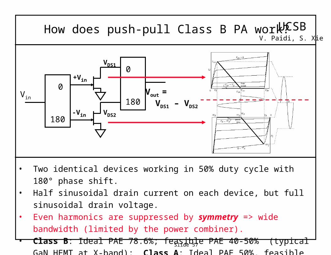
• Two identical devices working in 50% duty cycle with 180° phase shift. • Half sinusoidal drain current on each device, but full sinusoidal drain voltage. • Even harmonics are suppressed by symmetry => wide bandwidth (limited
by the power combiner). • Class B: Ideal PAE 78.6%; feasible PAE 40-50% (typical GaN HEMT at X-
band); Class A: Ideal PAE 50%, feasible PAE 20-30%.
VinVout = VDS1 – VDS2
0
180
0
180
+Vin
-Vin VDS2
VDS1
UCSBHow does push-pull Class B PA work?V. Paidi, S. Xie

Slide 58
Common Base Power Amplifier @40GHz
30 50 7010 80
-7.5-5.0-2.50.02.55.07.5
10.012.515.017.5
-10.0
20.0
freq, GHz
dB
(S(2
,1))
dB
(S(1
,1))
dB
(S(2
,2))
Technology:• InP mesa HBT•Ft~200 GHz, fmax ~400 GHz•Vbr ~ 7V•Current density ~ 3mA/um2•Area ~4 fingersX0.8X12 um2
Pout ~ 21 dBm
Approximate Layout (1.1 mm X0.3 mm) Performance gain > 10 dB
2 4 6 8 10 120 14
12
14
16
18
20
10
22
0.1
0.2
0.3
0.0
0.4
p
pout P
AE

Slide 59
Common Base Power Amplifier @60GHz
20 40 60 80 1000 110
-7.5-5.0-2.50.02.55.07.5
10.012.515.017.5
-10.0
20.0
freq, GHz
dB
(S(2
,1))
dB
(S(1
,1))
dB
(S(2
,2))
2 4 6 8 10 120 14
12
14
16
18
20
10
22
0.1
0.2
0.3
0.0
0.4
p
pout P
AE
Technology:• InP mesa HBT•Ft~200 GHz, fmax ~400 GHz•Vbr ~ 7V•Current density ~ 3mA/um2•Area ~4 fingersX0.8X12 um2
Pout > 21 dBm
Approximate Layout (0.7 mm X0.3 mm) Performance gain > 10 dB

Slide 60
Common Base Power Amplifier @80GHz
70 90 110 13050 150
-7.5-5.0-2.50.02.55.07.5
10.012.515.017.5
-10.0
20.0
freq, GHz
dB
(S(2
,1))
dB
(S(1
,1))
dB
(S(2
,2))
Technology:• InP mesa HBT•Ft~200 GHz, fmax ~400 GHz•Vbr ~ 7V•Current density ~ 3mA/um2•Area ~4 fingersX0.8X12 um2
Pout > 21 dBm
Approximate Layout (0.6 mm X0.3 mm) Performance gain > 10 dB
2 4 6 8 10 120 14
12
14
16
18
20
10
22
0.05
0.10
0.15
0.20
0.25
0.30
0.00
0.35
p
pout P
AE

Slide 61
Technology:• InP mesa HBT•Ft~200 GHz, fmax ~400 GHz•Vbr ~ 7V•Current density ~ 3mA/um2•Area ~4 fingersX0.8X12 um2
Pout > 20 dBm
Approximate Layout (0.5 mm X0.3 mm) Performance gain > 8 dB
2 4 6 8 10 120 14
10
12
14
16
18
20
8
22
0.05
0.10
0.15
0.20
0.00
0.25
p
pout P
AE
100 120 14080 150
-7.5-5.0-2.50.02.55.07.5
10.012.515.017.5
-10.0
20.0
freq, GHz
dB
(S(2
,1))
dB
(S(1
,1))
dB
(S(2
,2))
Common Base Power Amplifier @100GHz

Slide 62
Common Base Power Amplifier @120GHz
2 4 6 8 10 12 14 160 18
10
15
20
5
25
0.05
0.10
0.15
0.20
0.25
0.00
0.30
p
pout P
AE
80 100 12060 140
-7.5-5.0-2.50.02.55.07.5
10.012.515.017.5
-10.0
20.0
freq, GHz
dB
(S(2
,1))
dB
(S(1
,1))
dB
(S(2
,2))
Technology:• InP mesa HBT•Ft~200 GHz, fmax ~400 GHz•Vbr ~ 7V•Current density ~ 3mA/um2•Area ~4 fingersX0.8X12 um2
Pout > 20 dBm
Approximate Layout (0.5 mm X0.3 mm) Performance gain > 7 dB

Slide 63
Technology:• InP mesa HBT•Ft~200 GHz, fmax ~400 GHz•Vbr ~ 7V•Current density ~ 3mA/um2•Area ~2 fingersX0.8X12 um2
Pout > 16 dBm
Approximate Layout (0.5 mm X0.3 mm) Performance gain > 8 dB
Common Base Power Amplifier @140GHz
140 19090 240
-5
0
5
10
-10
15
freq, GHz
dB
(S(2
,1))
dB
(S(1
,1))
dB
(S(2
,2))
2 3 4 5 6 7 8 91 10
10
12
14
16
8
18
0.10
0.15
0.20
0.25
0.05
0.30
p
pout P
AE

Slide 64
Technology:• InP mesa HBT•Ft~200 GHz, fmax ~400 GHz•Vbr ~ 7V•Current density ~ 3mA/um2•Area ~2 fingersX0.8X12 um2
Pout > 16 dBm
Approximate Layout (0.4 mm X0.3 mm) Performance gain > 8 dB
Common Base Power Amplifier @160GHz
160 210110 260
-8-6-4-202468
101214
-10
15
freq, GHz
dB(S
(2,1
))dB
(S(1
,1))
dB(S
(2,2
))
2 3 4 5 6 7 8 91 10
8
10
12
14
16
6
18
0.05
0.10
0.15
0.20
0.00
0.25
p
pout P
AE

Slide 65
Technology:• InP mesa HBT•Ft~200 GHz, fmax ~400 GHz•Vbr ~ 7V•Current density ~ 3mA/um2•Area ~2 fingersX0.8X12 um2
Pout > 16 dBm
Approximate Layout (0.4 mm X0.3 mm) Performance gain ~ 5 dB
Common Base Power Amplifier @180GHz
140 19090 240
-5
0
5
10
-10
15
freq, GHz
dB
(S(2
,1))
dB
(S(1
,1))
dB
(S(2
,2))
2 4 6 8 100 12
6
8
10
12
14
16
4
18
0.05
0.10
0.15
0.00
0.20
p
pout P
AE

Slide 66
Technology:• InP mesa HBT•Ft~200 GHz, fmax ~400 GHz•Vbr ~ 7V•Current density ~ 3mA/um2•Area ~2 fingersX0.8X12 um2
Pout ~ 16 dBm
Approximate Layout (0.4 mm X0.3 mm) Performance gain ~ 5 dB
Common Base Power Amplifier @200GHz
140 19090 240
-5
0
5
10
-10
15
freq, GHz
dB(S
(2,1
))dB
(S(1
,1))
dB(S
(2,2
))
2 4 6 8 10 120 14
6
8
10
12
14
16
4
18
0.02
0.04
0.06
0.08
0.10
0.12
0.00
0.14
p
pout P
AE

Slide 67
Technology:• InP mesa HBT•Ft~200 GHz, fmax ~400 GHz•Vbr ~ 7V•Current density ~ 3mA/um2•Area ~2 fingersX0.8X12 um2
Pout ~ 15 dBm
Approximate Layout (0.3 mm X0.3 mm) Performance gain ~ 5 dB
Common Base Power Amplifier @220GHz
170 190 210 230 250 270150 290
-5
0
5
10
-10
15
freq, GHz
dB
(S(2
,1))
dB
(S(1
,1))
dB
(S(2
,2))
2 4 6 8 100 12
6
8
10
12
14
4
16
0.02
0.04
0.06
0.08
0.10
0.00
0.12
p
pout P
AE
Slide 68
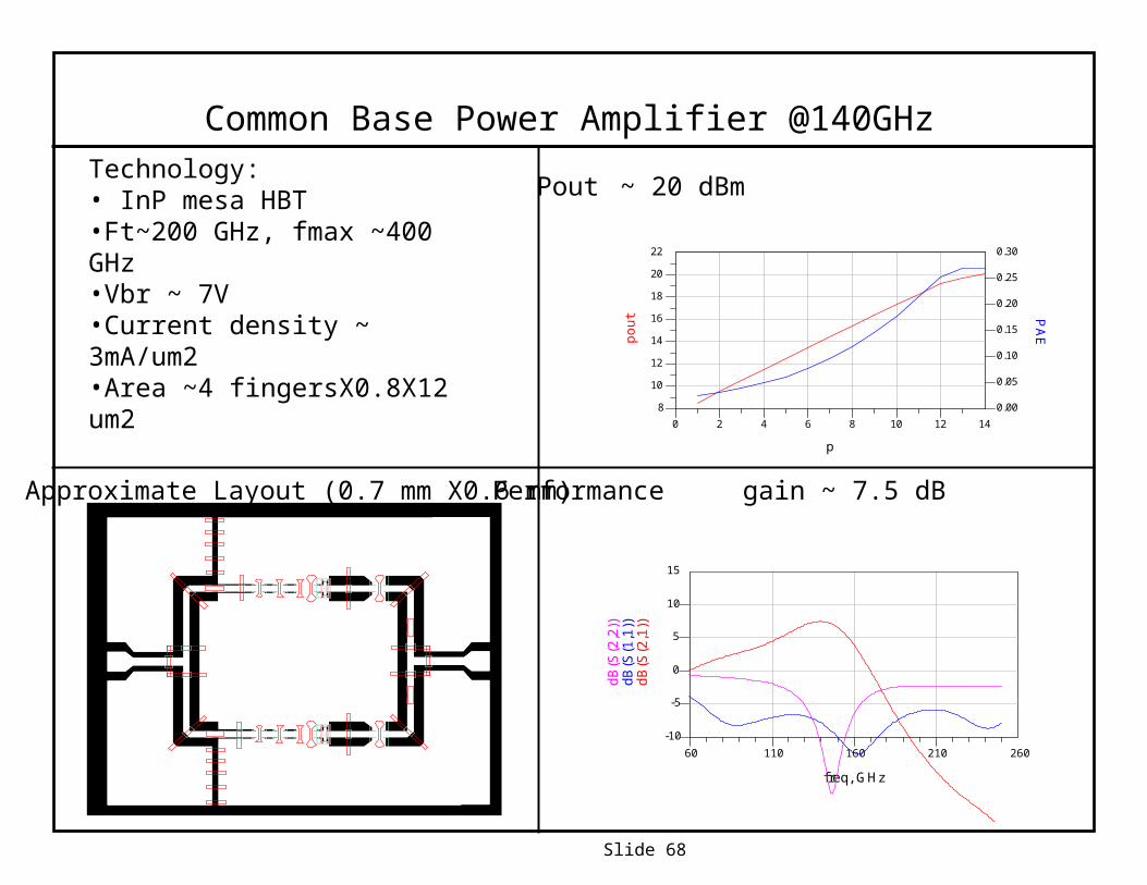
Technology:• InP mesa HBT•Ft~200 GHz, fmax ~400 GHz•Vbr ~ 7V•Current density ~ 3mA/um2•Area ~4 fingersX0.8X12 um2
Pout ~ 20 dBm
Approximate Layout (0.7 mm X0.6 mm) Performance gain ~ 7.5 dB
Common Base Power Amplifier @140GHz
110 160 21060 260
-5
0
5
10
-10
15
freq, GHz
dB
(S(2
,1))
dB
(S(1
,1))
dB
(S(2
,2))
2 4 6 8 10 120 14
10
12
14
16
18
20
8
22
0.05
0.10
0.15
0.20
0.25
0.00
0.30
p
pout P
AE

Slide 69
Technology:• InP mesa HBT•Ft~200 GHz, fmax ~400 GHz•Vbr ~ 7V•Current density ~ 3mA/um2•Area ~4 fingersX0.8X12 um2
Pout ~ 20 dBm
Approximate Layout (0.6 mm X0.5 mm) Performance gain ~ 6.8 dB
Common Base Power Amplifier @160GHz
140 19090 240
-5
0
5
10
-10
15
freq, GHz
dB
(S(2
,1))
dB
(S(1
,1))
dB
(S(2
,2))
2 4 6 8 10 12 140 16
8
10
12
14
16
18
6
20
0.05
0.10
0.15
0.00
0.20
p
pout P
AE

Slide 70
Technology:• InP mesa HBT•Ft~200 GHz, fmax ~400 GHz•Vbr ~ 7V•Current density ~ 3mA/um2•Area ~4 fingersX0.8X12 um2
Pout ~ 20 dBm
Approximate Layout (0.5 mm X0.5 mm) Performance gain ~ 5 dB
Common Base Power Amplifier @180GHz
140 19090 240
-5
0
5
10
-10
15
freq, GHz
dB(S
(2,1
))dB
(S(1
,1))
dB(S
(2,2
))
2 4 6 8 10 12 14 160 18
10
15
5
20
0.05
0.10
0.15
0.00
0.20
p
pout P
AE

Slide 71
Technology:• InP mesa HBT•Ft~200 GHz, fmax ~400 GHz•Vbr ~ 7V•Current density ~ 3mA/um2•Area ~4 fingersX0.8X12 um2
Pout ~ 19 dBm
Approximate Layout (0.5 mm X0.5 mm) Performance gain ~ 4.5 dB
Common Base Power Amplifier @200GHz
140 19090 240
-5
0
5
10
-10
15
freq, GHz
dB(S
(2,1
))dB
(S(1
,1))
dB(S
(2,2
))
2 4 6 8 10 12 14 160 18
10
15
5
20
0.05
0.10
0.00
0.15
p
pout P
AE

Slide 72
Technology:• InP mesa HBT•Ft~200 GHz, fmax ~400 GHz•Vbr ~ 7V•Current density ~ 3mA/um2•Area ~4 fingersX0.8X12 um2
Pout ~ 16 dBm
Approximate Layout (1 mm X0.7 mm) Performance gain ~ 15dB
Two-stage Common Base Power Amplifier @140GHz
-12 -10 -8 -6 -4 -2 0-14 2
5
10
15
0
20
p
pout
140 19090 240
-5
0
5
10
15
-10
18
freq, GHz
dB(S
(2,1
))dB
(S(1
,1))
dB(S
(2,2
))

Slide 73
Technology:• InP mesa HBT•Ft~200 GHz, fmax ~400 GHz•Vbr ~ 7V•Current density ~ 3mA/um2•Area ~6 fingersX0.8X12 um2
Pout ~ 20 dBm
Approximate Layout (1.3 mm X0.7 mm) Performance gain ~ 15dB
Two-stage Common Base Power Amplifier @140GHz
110 130 15090 170
-5
0
5
10
15
-10
18
freq, GHz
dB
(S(2
,1))
dB
(S(1
,1))
dB
(S(2
,2))
-12 -10 -8 -6 -4 -2 0 2 4 6-14 8
5
10
15
20
0
25
p
pout

Slide 74
Technology:• InP mesa HBT•Ft~200 GHz, fmax ~400 GHz•Vbr ~ 7V•Current density ~ 3mA/um2•Area ~4 fingersX0.8X12 um2
Pout ~ 16.5 dBm
Approximate Layout (1.3 mm X0.7 mm)Performance gain ~ 10dB
Two-stage Common Base Power Amplifier @180GHz
140 160 180 200 220120 230
-5
0
5
10
15
-10
18
freq, GHz
dB(S
(2,1
))dB
(S(1
,1))
dB(S
(2,2
))
1 2 3 4 5 6 70 8
12
14
16
10
18
p
pout

Slide 75
Technology:• InP mesa HBT•Ft~200 GHz, fmax ~400 GHz•Vbr ~ 7V•Current density ~ 3mA/um2•Area ~6 fingersX0.8X12 um2
Pout ~ 20 dBm
Approximate Layout (1.3 mm X0.7 mm) Performance gain ~ 8.5dB
Two-stage Common Base Power Amplifier @180GHz
140 160 180 200 220120 230
-5
0
5
10
15
-10
18
freq, GHz
dB
(S(2
,1))
dB
(S(1
,1))
dB
(S(2
,2))
1 2 3 4 5 6 7 8 9 10 110 12
10
12
14
16
18
8
20
p
pout

Slide 76
Technology:• InP mesa HBT•Ft~200 GHz, fmax ~400 GHz•Vbr ~ 7V•Current density ~ 3mA/um2•Area ~4 fingersX0.8X12 um2
Pout ~ 16.5 dBm
Approximate Layout (1.3 mm X0.7 mm) Performance gain ~ 10dB
Two-stage Common Base Power Amplifier @200GHz
180 200 220 240160 260
-5
0
5
10
15
-10
18
freq, GHz
dB
(S(2
,1))
dB
(S(1
,1))
dB
(S(2
,2))
1 2 3 4 5 6 70 8
12
14
16
10
18
p
pout

Slide 77
Technology:• InP mesa HBT•Ft~200 GHz, fmax ~400 GHz•Vbr ~ 7V•Current density ~ 3mA/um2•Area ~4 fingersX0.8X12 um2
Pout > 17 dBm
Approximate Layout (0.5 mm X0.6 mm) Performance gain ~ 8dB
Cascode Power Amplifier @140GHz
-8 -6 -4 -2 0 2 4 6 8-10 10
0
5
10
15
-5
20
0.1
0.2
0.3
0.0
0.4
p
pout P
AE
90 14040 180
-5
0
5
10
-10
15
freq, GHz
dB
(S(2
,1))
dB
(S(1
,1))
dB
(S(2
,2))

Slide 78
140 160 180 200 220120 240
-5
0
5
10
15
-10
18
freq, GHz
dB
(S(2
,1))
dB
(S(1
,1))
dB
(S(2
,2))
Technology:• InP mesa HBT•Ft~200 GHz, fmax ~400 GHz•Vbr ~ 7V•Current density ~ 3mA/um2•Area ~4 fingersX0.8X12 um2
Pout ~ 16.5 dBm
Approximate Layout (0.5 mm X0.6 mm) Performance gain ~ 8dB
Cascode Power Amplifier @180GHz
-4 -3 -2 -1 0 1 2 3 4 5 6 7 8 9 10 11-5 12
0
5
10
15
-5
20
p
pout

Slide 79
Technology:• InP mesa HBT•Ft~200 GHz, fmax ~400 GHz•Vbr ~ 7V•Current density ~ 3mA/um2•Area ~4 fingersX0.8X12 um2
Pout ~ 19 dBm
Approximate Layout (0.5 mm X0.3 mm) Performance gain ~ 8dB
Common Base Power Amplifier (No Cap design) @100GHz
80 100 12060 140
-7.5-5.0-2.50.02.55.07.5
10.012.515.017.5
-10.0
20.0
freq, GHz
dB
(S(2
,1))
dB
(S(1
,1))
dB
(S(2
,2))
2 4 6 8 10 120 14
10
12
14
16
18
8
20
0.05
0.10
0.15
0.20
0.25
0.30
0.00
0.35
p
pout P
AE

Slide 80
Technology:• InP mesa HBT•Ft~200 GHz, fmax ~400 GHz•Vbr ~ 7V•Current density ~ 3mA/um2•Area ~2 fingersX0.8X12 um2
Pout ~ 15.5 dBm
Approximate Layout (0.5 mm X0.3 mm) Performance gain ~ 7dB
Common Base Power Amplifier (No Cap design) @140GHz
2 4 6 8 10 120 14
10
12
14
8
16
0.06
0.08
0.10
0.12
0.14
0.04
0.16
p
pout P
AE
120 140 160 180100 190
-7.5-5.0-2.50.02.55.07.5
10.012.515.017.5
-10.0
20.0
freq, GHz
dB
(S(2
,1))
dB
(S(1
,1))
dB
(S(2
,2))

Slide 81
Technology:• InP mesa HBT•Ft~200 GHz, fmax ~400 GHz•Vbr ~ 7V•Current density ~ 3mA/um2•Area ~2 fingersX0.8X12 um2
Pout ~ 16 dBm
Approximate Layout (0.3 mm X0.3 mm) Performance gain ~ 5dB
Common Base Power Amplifier (No Cap design) @180GHz
170 190 210150 220
-7.5-5.0-2.50.02.55.07.5
10.012.515.017.5
-10.0
20.0
freq, GHz
dB
(S(2
,1))
dB
(S(1
,1))
dB
(S(2
,2))
2 4 6 8 10 120 14
6
8
10
12
14
4
16
0.04
0.06
0.08
0.10
0.12
0.14
0.02
0.16
p
pout P
AE

Slide 82
Technology:• InP mesa HBT•Ft~200 GHz, fmax ~400 GHz•Vbr ~ 7V•Current density ~ 3mA/um2•Area ~2 fingersX0.8X12 um2
Pout ~ 16 dBm
Approximate Layout (0.3 mm X0.3 mm) Performance gain ~ 4dB
2 4 6 8 10 120 14
6
8
10
12
14
4
16
0.02
0.04
0.06
0.08
0.10
0.12
0.00
0.14
p
pout P
AE
Common Base Power Amplifier (No Cap design) @200GHz
170 190 210150 220
-7.5-5.0-2.50.02.55.07.5
10.012.515.017.5
-10.0
20.0
freq, GHz
dB
(S(2
,1))
dB
(S(1
,1))
dB
(S(2
,2))

Slide 83
Technology:• InP mesa HBT•Ft~200 GHz, fmax ~400 GHz•Vbr ~ 7V•Current density ~ 3mA/um2•Area ~4 fingersX0.8X12 um2
Pout > 16 dBm
Approximate Layout (0.3 mm X0.3 mm) Performance gain ~ 10dB
Two-stage Common Base Power Amplifier (No Cap design) @180GHz
170 190 210150 220
-7.5-5.0-2.50.02.55.07.5
10.012.515.017.5
-10.0
20.0
freq, GHz
dB
(S(2
,1))
dB
(S(1
,1))
dB
(S(2
,2))
2 3 4 5 6 7 8 91 10
12
13
14
15
16
11
17
-0.5
0.0
0.5
-1.0
1.0
p
pout
nothing
PA
E <
inva
lid>

Slide 84
Thermal Structures--- 18 um gate length device with three partitions 0,4,8

Slide 85
Thermal Structures --- 2 finger device with 0,4,8 ballasting(0.8X12)

Slide 86
GaN HEMT Model

Slide 87
GaN HEMT Model Contd.-Gm block
Variables -------- gm, ft, vp, fudfactor(0.05 here)---- automatic Gds modeling. Probably
more accurate.

Slide 88
GaN HEMT Model Contd.-Gm blocka discussion
The Id-Vds characteristics do not show any changeOf pinch-off voltage till Vds ~ 7-10 V. Then there wouldBe a shift of 0.5-1 V per every 10V Vds increase.
This has been more accurately modeled in this new Device model.

Slide 89
GaN HEMT Model Contd.-Gm blocka discussion
The Id-Vds characteristics of a 1.2 mm device.
2 4 6 8 10 12 14 16 18 20 22 240 26
0.20.40.60.81.01.21.4
0.0
1.6
Vds, V
Dra
in C
urre
nt, A

Slide 90
GaN HEMT Model Contd.-Gm blocka discussion
The Id-Vgs characteristics of a 1.2 mm device at Vds= 15V.
-8 -7 -6 -5 -4 -3 -2 -1-9 0
0.3
0.6
0.9
1.2
0.0
1.5
Vgs, V
Dra
in C
urre
nt, A

Slide 91
GaN HEMT Model Contd.-Cgs

Slide 92
GaN HEMT Model Contd.-Cgs
The Id-Vgs characteristics of a 1.2 mm device at Vds= 15V.
-8 -7 -6 -5 -4 -3-9 -2
0.70.80.91.0
0.6
1.1
Vgs, V
Cgs
, pF

Slide 93
GaN HEMT Model Contd.-Cgs
The S-parameter match of SG device at -4V Vgs, 20V VdsModel could be fine tuned. But my point is that this model is Not way off.

Slide 94
Dual Gate device and linearity concerns.
The Common Source Power Amplifier Circuit:

Slide 95
Dual Gate device and linearity concerns.
model:

Slide 96
Dual Gate device and linearity concerns.One step at a time ---- Only Gm non-linearity
model:

Slide 97
Dual Gate device and linearity concerns.One step at a time ---- Only Gm non-linearity
Biased at Class B -6V here:
24 26 28 30 32 34 3622 38
15
30
45
60
75
0
90
Total output power, dBm
IM3
supp
ress
ion,
dB
c

Slide 98
Dual Gate device and linearity concerns.One step at a time ---- Only Gm non-linearity
Biased at Class C -7V here:
14 16 18 20 22 24 26 28 30 32 34 3612 38
15
30
45
60
75
0
90
Total output power, dBm
IM3
supp
ress
ion,
dB
c

Slide 99
Dual Gate device and linearity concerns.One step at a time ---- Only Gm non-linearity
Biased at Class AB -4.5V here:
24 26 28 30 32 34 3622 38
15
30
45
60
75
0
90
Total output power, dBm
IM3
supp
ress
ion,
dB
c

Slide 100
Dual Gate device and linearity concerns.One step at a time ---- Only Gm non-linearity
Biased at Class A -3V here:
24 26 28 30 32 34 3622 38
153045607590
105
0
120
Total output power, dBm
IM3
supp
ress
ion,
dB
c

Slide 101
Dual Gate device and linearity concerns.One step at a time ---- Gm+Cgs non-linearity
model:

Slide 102
Dual Gate device and linearity concerns.One step at a time ---- Gm+Cgs non-linearity
Biased at Class B -6V:
22 24 26 28 30 32 34 3620 38
15
30
45
0
60
Total output power, dBm
IM3
supp
ress
ion,
dB
c

Slide 103
Dual Gate device and linearity concerns.One step at a time ---- Gm+Cgs non-linearity
Biased at Class C -7V:
15 20 25 30 3510 40
15
30
45
0
60
Total output power, dBm
IM3
supp
ress
ion,
dB
c

Slide 104
Dual Gate device and linearity concerns.One step at a time ---- Gm+Cgs non-linearity
Biased at Class AB -4.5V:
15 20 25 30 3510 40
15
30
45
0
60
Total output power, dBm
IM3
supp
ress
ion,
dB
c

Slide 105
Dual Gate device and linearity concerns.One step at a time ---- Gm+Cgs non-linearity
Biased at Class AB -3 V:
15 20 25 30 3510 40
15
30
45
60
75
0
90
Total output power, dBm
IM3
supp
ress
ion,
dB
c

Slide 106
Dual Gate device and linearity concerns.One step at a time ---- Gm+Cgs+Vp shift non-linearity
model:

Slide 107
Dual Gate device and linearity concerns.One step at a time ---- Gm+Cgs+Vp shift non-linearity
Class B -6.1 V The rest does not change that much:
15 20 25 30 3510 40
15
30
45
60
75
0
90
Total output power, dBm
IM3
supp
ress
ion,
dB
c

Slide 108
Single Gate device and linearity concerns.
Common source Circuit Design

Slide 109
Single Gate device and linearity concerns.
Common drain Circuit Design

Slide 110
Single Gate device and linearity concerns.One Step at a time --- Only Gm nonlinearity
Model:

Slide 111
Single Gate device and linearity concerns.One Step at a time --- Only Gm nonlinearity
Class B -6V:
10 15 20 25 30 355 40
20406080
100
0
120
Total Output Power, dBm
Im3
supp
ress
ion,
dB
c

Slide 112
Single Gate device and linearity concerns.One Step at a time --- Only Gm nonlinearity
Class C -7V:
20 25 30 3515 40
15
30
45
0
60
Total Output Power, dBm
Im3
supp
ress
ion,
dB
c

Slide 113
Single Gate device and linearity concerns.One Step at a time --- Only Gm nonlinearity
Class AB -4.5V:
20 25 30 3515 40
15
30
45
0
60
Total Output Power, dBm
Im3
supp
ress
ion,
dB
c

Slide 114
Single Gate device and linearity concerns.One Step at a time --- Only Gm nonlinearity
Class A -3V:
20 25 30 3515 40
153045607590
0
100
Total Output Power, dBm
Im3
supp
ress
ion,
dB
c

Slide 115
Single Gate device and linearity concerns.One Step at a time --- Gm+Cgs nonlinearity
model:

Slide 116
Single Gate device and linearity concerns.One Step at a time --- Gm+Cgs nonlinearity
Class B -6V:
20 25 30 3515 40
153045607590
0
100
Total Output Power, dBm
Im3
supp
ress
ion,
dB
c

Slide 117
Single Gate device and linearity concerns.One Step at a time --- Gm+Cgs nonlinearity
Class C -7V:
20 25 30 3515 40
153045607590
0
100
Total Output Power, dBm
Im3
supp
ress
ion,
dB
c

Slide 118
Single Gate device and linearity concerns.One Step at a time --- Gm+Cgs nonlinearity
Class AB -4.5V:
20 25 30 3515 40
153045607590
0
100
Total Output Power, dBm
Im3
supp
ress
ion,
dB
c

Slide 119
Single Gate device and linearity concerns.One Step at a time --- Gm+Cgs nonlinearity
Class AB -3V:
20 25 30 3515 40
153045607590
0
100
Total Output Power, dBm
Im3
supp
ress
ion,
dB
c

Slide 120
Single Gate device and linearity concerns.One Step at a time --- Gm+Cgs+Vpshift nonlinearitymodel:

Slide 121
Single Gate device and linearity concerns.One Step at a time --- Gm+Cgs+Vpshift nonlinearityClass B -6.5V:
20 25 30 3515 40
1020304050
0
60
Total Output Power, dBm
Im3
supp
ress
ion,
dB
c

Slide 122
Single Gate device and linearity concerns.One Step at a time --- Gm+Cgs+Vpshift nonlinearityClass C -7.5V:
20 25 30 3515 40
1020304050
0
60
Total Output Power, dBm
Im3
supp
ress
ion,
dB
c

Slide 123
Single Gate device and linearity concerns.One Step at a time --- Gm+Cgs+Vpshift nonlinearityClass AB -4.5V:
20 25 30 3515 40
1020304050
0
60
Total Output Power, dBm
Im3
supp
ress
ion,
dB
c

Slide 124
Single Gate device and linearity concerns.One Step at a time --- Gm+Cgs+Vpshift nonlinearityClass A -3V:
20 25 30 3515 40
1020304050
0
60
Total Output Power, dBm
Im3
supp
ress
ion,
dB
c

Slide 125
Common Drain Circuit on chip right now!
Circuit Diagram (slightly modified):

Slide 126
Common Drain Circuit on chip right now!
Class B -6.5V
16 18 20 22 24 26 28 30 32 34 3614 38
10
20
30
40
50
0
60
total output power, dBm
IM3
supp
ress
ion,
dB
c

Slide 127
Common Drain Circuit on chip right now!
Class C -7.5V
8 10 12 14 16 18 20 22 24 26 28 30 32 34 366 38
10
20
30
40
50
0
60
total output power, dBm
IM3
supp
ress
ion,
dB
c

Slide 128
Common Drain Circuit on chip right now!
Class AB -4.5V
18 20 22 24 26 28 30 32 34 3616 38
10
20
30
40
50
0
60
total output power, dBm
IM3
supp
ress
ion,
dB
c

Slide 129
Common Drain Circuit on chip right now!
Class A -3V
18 20 22 24 26 28 30 32 34 3616 38
10
20
30
40
50
0
60
total output power, dBm
IM3
supp
ress
ion,
dB
c

Slide 130
Common Drain Circuit on chip right now!
Class B -6.5V--- Two tone simulation
5 10 15 20 250 30
-20
-10
0
10
20
30
-30
40
Total Output Power, dBm
Out
put P
ower
, 5G
Hz,
dB
m

Slide 131
Class B two-tone output spectrum
-60
-40
-20
0
20
40
7.998 7.999 8 8.001 8.002 8.003
Outp
ut
spectr
um
, dB
m
Freq, GHz
-60
-40
-20
0
20
40
7.998 7.999 8 8.001 8.002 8.003
Out
put
spec
trum
, dB
m
Freq, GHz
-60
-40
-20
0
20
40
7.998 7.999 8 8.001 8.002 8.003
Out
put
spec
trum
, dB
m
Freq, GHz
-60
-40
-20
0
20
40
7.998 7.999 8 8.001 8.002 8.003
Out
put
spec
trum
, dB
m
Freq, GHz
Pout = 4 dBm
IM3 = 43 dBc
Low input power
Medium input power 1
Medium input power 2 High input power
Pout =18 dBm
IM3 = 39 dBc
Pout = 22 dBm
IM3 = 40 dBc
Pout = 26 dBm
IM3 = 25 dBc

Slide 132
Class A two-tone output spectrum
-60
-40
-20
0
20
40
7.998 7.999 8 8.001 8.002 8.003
Out
put
spec
trum
, dB
m
Freq, GHz
-60
-40
-20
0
20
40
7.998 7.999 8 8.001 8.002 8.003
Out
put
spec
trum
, dB
m
Freq, GHz
-60
-40
-20
0
20
40
7.998 7.999 8 8.001 8.002 8.003
Out
put
spec
trum
, dB
m
Freq, GHz
Pout = 10 dBm
IM3 > 50 dBc
Pout = 27 dBm
IM3 = 31 dBc Pout = 31 dBm
IM3 = 15 dBc
Low input power
Medium input power 2 High input power
-60
-40
-20
0
20
40
7.998 7.999 8 8.001 8.002 8.003
Out
put
spec
trum
, dB
m
Freq, GHz
Medium input power 2
Pout = 23 dBm
IM3 = 42 dBc