SIMULATING THE EFFECTS OF MECHANICAL …...12= 12+( 11− 12− 44)( 12 22+ 12 22+ 12 22) (2-4)...
42
SIMULATING THE EFFECTS OF MECHANICAL STRESS ON HALL-EFFECT SENSOR DEVICES By NATHAN MILLER A THESIS PRESENTED TO THE COLLEGE OF ENGINEERING OF THE UNIVERSITY OF FLORIDA IN PARTIAL FULFILLMENT OF THE REQUIREMENTS FOR THE DEGREE OF BACHELOR OF SCIENCE SUMMA CUM LAUDE UNIVERSITY OF FLORIDA 2019
Transcript of SIMULATING THE EFFECTS OF MECHANICAL …...12= 12+( 11− 12− 44)( 12 22+ 12 22+ 12 22) (2-4)...
SIMULATING THE EFFECTS OF MECHANICAL STRESS
ON HALL-EFFECT SENSOR DEVICES
By
NATHAN MILLER
A THESIS PRESENTED TO THE COLLEGE OF ENGINEERING
OF THE UNIVERSITY OF FLORIDA IN PARTIAL FULFILLMENT
OF THE REQUIREMENTS FOR THE DEGREE OF
BACHELOR OF SCIENCE SUMMA CUM LAUDE
UNIVERSITY OF FLORIDA
2019
To my Mom and Dad, Kirstin, and Logan

3
ACKNOWLEDGMENTS
I would like to thank my advisor, Dr. Mark Law, for taking me on as an undergraduate
researcher nearly three years ago, for his continual support, and for his endless guidance through
the past several years. My sincere thanks also go to Dr. Keith Green and Dr. Aravind
Appaswamy, our closest contacts from Texas Instruments on this project, as well as other
contributors from TI; my colleagues Dr. Madeline Sciullo, Henry Johnson, and Thomas
Weingartner who each contributed immensely to this project; my committee members Dr. Erin
Patrick and Dr. James Keesling; and my lab mates Dr. Shrijit Mukherjee, Bobby, Lars, Nimesh,
Ribhu and Marquita.
I would also like to thank my parents for always supporting me and pushing me to be the
best I can be, and my brother and sister for their love and support. I would like to thank my
friends Zach, Robert, Logan, Kyle, Mitch, and Dane for their brotherhood through the years; my
colleagues and friends from Eta Kappa Nu Epsilon Sigma; my microchurch community for their
prayers and support; and Skyler, Aamir, Carina, Daniel, Nicole, Madison, John, Dan, Cristina,
and the many others who have influenced my journey.
Above all, I would like to thank God for His providence in getting me to where I am
today.
4
TABLE OF CONTENTS
page
ACKNOWLEDGMENTS ...............................................................................................................3
LIST OF TABLES ...........................................................................................................................5
LIST OF FIGURES .........................................................................................................................6
ABSTRACT .....................................................................................................................................7
INTRODUCTION ...........................................................................................................................8
BACKGROUND AND INTRODUCTION TO HALL-EFFECT SENSORS ................................9
SIMULATIONS TOOLS AND MODELS ...................................................................................15
RESULTS ......................................................................................................................................17
Resistance Changes Due to Mechanical Stress ......................................................................17 Offset Voltage Changes Due to Mechanical Stress ................................................................19 Using Electron Mobility and Electrostatic Potential Changes to Understand Trends ............20
CONCLUSIONS AND FUTURE WORK ....................................................................................38
Summary of Findings .............................................................................................................38 Future Work ............................................................................................................................38
LIST OF REFERENCES ...............................................................................................................40
BIOGRAPHICAL SKETCH .........................................................................................................41
5
LIST OF TABLES
Table page
Table 1-1. Piezoresistance components at room temperature in units of 10-12 cm2/dyne .............14
6
LIST OF FIGURES
Figure page
Figure 2-1. The Hall-effect sensor devices studied in this work. .................................................12
Figure 2-2. A graphical depiction of the Hall-effect.....................................................................12
Figure 2-3. A graphical depiction of the values of the piezoresistance coefficients for n-Si .......13
Figure 2-4. A graphical depiction of Euler’s angles .....................................................................14
Figure 3-1. Images displaying the mesh density used for the square and cross devices. .............16
Figure 4-1. Resistance results for the default cross structure with increasing stress. ...................24
Figure 4-2. Resistance results for the default square structure with increasing stress ..................25
Figure 4-3. Resistance results for the rotated cross structure with increasing stress ....................26
Figure 4-4. Resistance results for the rotated square structure with increasing stress ..................27
Figure 4-5. Summary of offset voltage results for the <100> square structure ............................28
Figure 4-6. Offset voltage results for the square device in various orientations. .........................29
Figure 4-7. Offset voltage results for the cross device in various orientations. ............................31
Figure 4-8. Changes in electron mobility and electrostatic potential for the <100> square
structure at various levels of stress ....................................................................................33
Figure 4-9. Changes in electron mobility and electrostatic potential for the <100> square
structure at 200MPa with various orientations. .................................................................34
Figure 4-10. Changes in electron mobility and electrostatic potential for the <110> square
structure at 200MPa with various orientations ..................................................................35
Figure 4-11. Changes in electron mobility and electrostatic potential for the <100> cross
structure at 200MPa with various orientations. .................................................................36
Figure 4-12. Changes in electron mobility and electrostatic potential for the <110> cross
structure at 200MPa with various orientations ..................................................................37
7
Abstract of Thesis Presented to the College of Engineering
of the University of Florida in Partial Fulfillment of the
Requirements for the Bachelor of Science Summa Cum Laude
SIMULATING THE EFFECTS OF MECHANICAL STRESS
ON HALL-EFFECT SENSOR DEVICES
By
Nathan Miller
May 2019
Chair: Mark E. Law
Major: Electrical Engineering
This work presents a study on the effects of mechanical stress on n-type Silicon Hall-
effect sensor devices. Device modeling performed in Sentaurus Device of mobility changes
through piezoresistive effects is used to analyze and understand experimentally observed
changes in device resistance and offset voltage in such devices. Relationships between crystal
orientation, stress direction, and current direction are observed and defined, wherein an offset
voltage is created in a Hall-effect device due to mechanical stress only when an asymmetry
exists in the electron mobility of the device across the axis of the driving current direction.
Future goals discovered through this work are outlined, as current Sentaurus Device
models are incapable of coupling mobility changes using the piezoresistive model and the Hall-
effect simultaneously for a study of the piezo-Hall effect. Studying the source of mechanical
stress through packaging and how to adequately model and account for it are crucial next steps
that industry partners need for improved device performance.
8
CHAPTER 1
INTRODUCTION
Mechanical stress affects semiconductor devices of all types, so it is of great interest to
better understand and predict the influence of package-induced stresses. In particular, silicon-
based devices can be significantly affected by stress due to the piezoresistive nature of silicon.
These effects can have negative impact on the accuracy of devices such as Hall-effect sensors.
These sensors measure a potential difference produced across the device in the presence of an
applied magnetic field with a component orthogonal to the flow of bias current. Mechanical
stress is known to influence charge carrier mobility [1]. This therefore can affect the potential
difference produced by a magnetic field, causing the device to produce inaccurate readings of
magnetic field intensity. These inaccurate readings have been measured in industry applications
by Texas Instruments, leading them to a particular interest in how mechanical stress effects on
Hall-effect sensors can be modeled and understood. By better understanding the sources of
mechanical stress and its effects, methods of counteracting or even utilizing its effects can be
developed in order to create more accurate and novel products for the end consumer. With the
widespread applications that the effects of mechanical stress can have on all sorts of
semiconductor devices, there are many possibilities for the use of this work across the
semiconductor industry.
9
CHAPTER 2
BACKGROUND AND INTRODUCTION TO HALL-EFFECT SENSORS
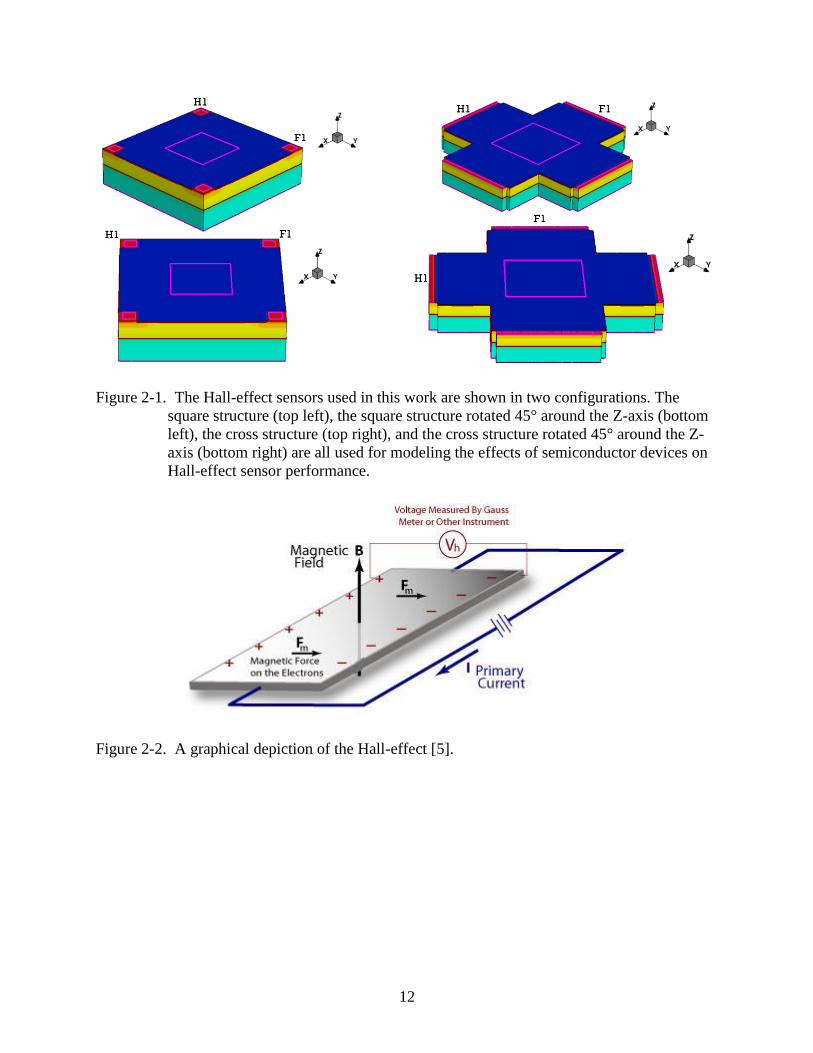
Figure 2-1 shows four configurations of the Hall-effect sensor devices used in this work.
The original devices which are commonly referred to as the “square” and “cross” are shown at
the top of the figure, and identical devices rotated 45° around the Z-axis are shown below them.
Generally, the current flowing through the device is driven by the terminal named “Force1,”
which is abbreviated as “F1” and shown in the figure. Current driven from Force1 flows across
the device to the “Force2” terminal directly opposite from Force1. The resistance of the device is
then calculated by dividing the voltage across the two driving terminals by the current through
them. The remaining two terminals of the device are named the “Hall1” (abbreviated “H1” in the
figure) and “Hall2” terminals, across which the Hall voltage is measured. The direction of the
current flow across the device can then be varied such that any of the four terminals of the device
can drive current, which will flow to the terminal on the opposite corner of the device. For
example, if current were driven from the terminal named “Hall1,” then the drive current would
flow towards “Hall2” and the true Hall-effect voltage would be the voltage measured between
the Force1 and Force2 terminals.
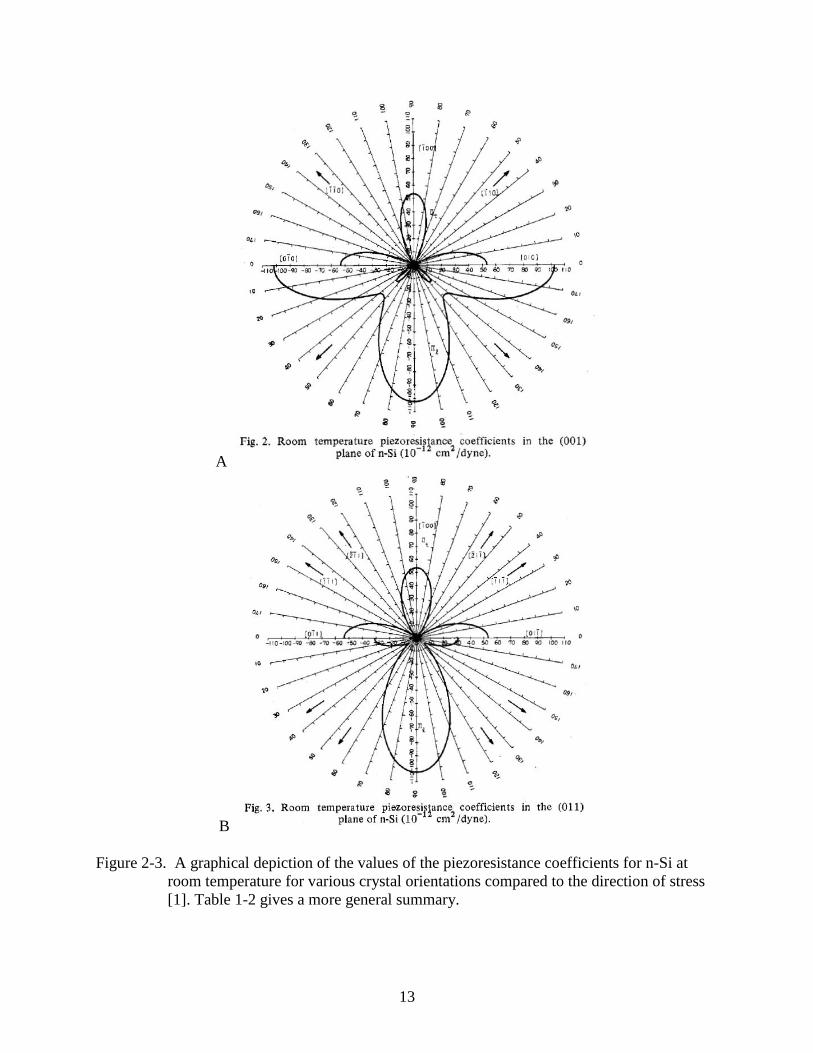
The Hall voltage across the non-driving terminals is produced by the presence of a
magnetic field shown in Equation 2-1 which serves to bend current out of its straight path
(similar to the image shown in Figure 2-2) between Force1 and Force2 to produce a voltage on
the Hall terminals.
𝐹𝑏 = q𝑉𝑑 𝑥 𝐵 (2-1)
Under typical operation, the voltage measured across these terminals can be used to
calculate the intensity of the ambient magnetic field present around the sensor. In the presence of
stress, however, a voltage across these terminals can be created which is referred to as the “offset
10
voltage.” The offset voltage is defined as the voltage across the Hall terminals in the absence of
magnetic field. This offset voltage in Hall-effect sensors leads to the measurement of a false
magnetic field when there is none present.
The principle effect of mechanical stress analyzed in this work is the piezoresistive effect,
which is defined as the change in resistivity in a semiconductor (in this case, silicon) when
mechanical stress is applied. This change in resistivity follows a series of equations outlined by
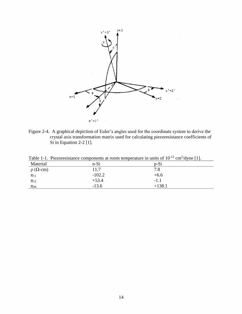
Yozo Kanda [1] and is highly dependent on the orientation of crystal axes, stress, and current
with respect to each other. Figure 2-2 shows a plot from Kanda’s paper which summarizes the
relationship between stress and crystal orientation on the piezoresistive coefficients for n-type
silicon for devices with <100> and <110> crystal orientations at room temperature. The
mathematics describing this transformation are described in Equations 2-2, 2-3 and 2-4. Note in
Equation 2-2 that, for brevity, cosine is abbreviated as “c” and sine is abbreviated as “s.” These
equations are derived by Kanda to produce the plots shown in Figure 2-3. The definitions of the
ϕ, θ and ψ angles are shown in Figure 2-4.
[
𝑙1 𝑚1 𝑛1
𝑙2 𝑚2 𝑛2
𝑙3 𝑚3 𝑛3
]
= [
c(𝜙) c(𝜃) s(𝜓) − s(𝜙) s(𝜓) s(𝜙) c(𝜃) c(𝜓) + c(𝜙) s(𝜓) − s(𝜃) s(𝜓)
− c(𝜙) c(𝜃) s(𝜓) − s(𝜙) s(𝜓) −s(𝜙) c(𝜃) s(𝜓) + c(𝜙) c(𝜓) s(𝜃) s(𝜓)
c(𝜙) s(𝜃) 𝑠(𝜙)𝑠(𝜃) 𝑐(𝜃)
]
(2-2)
Equation 2-2 displays the transformation matrix used for finding the longitudinal and
transverse piezoresistive coefficients.
𝜋′11 = 𝜋11 − 2(𝜋11 − 𝜋12 − 𝜋44)(𝑙1
2𝑚12 + 𝑚1
2𝑛12 + 𝑛1
2𝑙12)
(2-3)
Equation 2-3 yields the longitudinal piezoresistive coefficient, 𝜋′11, which is the
piezoresistive coefficient used when stress is parallel to the direction of current.
11
𝜋′12 = 𝜋12 + (𝜋11 − 𝜋12 − 𝜋44)(𝑙1
2𝑙22 + 𝑚1
2𝑚22 + 𝑛1
2𝑛22)
(2-4)
Equation 2-4 yields the transverse piezoresistive coefficient, 𝜋′12, which is the
piezoresistive coefficient used when stress is perpendicular to the direction of current.
𝛥𝜌𝜔
𝜌= ∑ 𝜋′
𝜔𝜆𝑋𝜆
6
𝜆=1
=
[ 𝜋11
′ 𝜋12′ 𝜋12
′
𝜋12′ 𝜋11
′ 𝜋12′
𝜋12′ 𝜋12
′ 𝜋11′
0 0 00 0 00 0 0
0 0 0 0 0 0 0 0 0
𝜋44 0 00 𝜋44 00 0 𝜋44]
[ 𝑆𝑥𝑥
𝑆𝑦𝑦
𝑆𝑧𝑧
𝑆𝑥𝑦
𝑆𝑧𝑥
𝑆𝑧𝑦]
=
[ 𝜋11
′ 𝑆𝑥𝑥 + 𝜋12′ 𝑆𝑦𝑦 + 𝜋12
′ 𝑆𝑧𝑧
𝜋12′ 𝑆𝑥𝑥 + 𝜋11
′ 𝑆𝑦𝑦 + 𝜋12′ 𝑆𝑧𝑧
𝜋12′ 𝑆𝑥𝑥 + 𝜋12
′ 𝑆𝑦𝑦 + 𝜋11′ 𝑆𝑧𝑧
𝜋44𝑆𝑥𝑦
𝜋44𝑆𝑧𝑥
𝜋44𝑆𝑧𝑦 ]
(2-5)
The end result of Kanda’s derivation for converting applied stress to a change in
resistivity is shown in Equation 2-5. All of the results analyzed in this study are produced by
applying a compressive stress in the X direction (referred to as Sxx) on the cross and square
devices shown in Figure 2-1. Therefore, current flowing in the X direction will be affected by the
resistivity changes from the longitudinal piezoresistive coefficient, and current flowing in the Y
and Z directions will be affected by the resistivity changes from the transverse piezoresistive
coefficient. Note that 𝜋44 refers to the piezoresistive component induced from shear stress,
which is not tested here due to the difficulty of applying a shear stress to a silicon wafer.
12
Figure 2-1. The Hall-effect sensors used in this work are shown in two configurations. The
square structure (top left), the square structure rotated 45° around the Z-axis (bottom
left), the cross structure (top right), and the cross structure rotated 45° around the Z-
axis (bottom right) are all used for modeling the effects of semiconductor devices on
Hall-effect sensor performance.
Figure 2-2. A graphical depiction of the Hall-effect [5].
13
A
B
Figure 2-3. A graphical depiction of the values of the piezoresistance coefficients for n-Si at
room temperature for various crystal orientations compared to the direction of stress
[1]. Table 1-2 gives a more general summary.
14
Figure 2-4. A graphical depiction of Euler’s angles used for the coordinate system to derive the
crystal axis transformation matrix used for calculating piezoresistance coefficients of
Si in Equation 2-2 [1].
Table 1-1. Piezoresistance components at room temperature in units of 10-12 cm2/dyne [1].
Material n-Si p-Si
ρ (Ω-cm) 11.7 7.8
π11 -102.2 +6.6
π12 +53.4 -1.1
π44 -13.6 +138.1
15
CHAPTER 3
SIMULATIONS TOOLS AND MODELS
The models to be modified and utilized in this study are created in Sentaurus Device, a
finite volume analysis software developed by Synopsys. Sentaurus simulates characteristics of
semiconductor devices using the Scharfetter-Gummel method [4], creating a tetrahedral mesh
and calculating characteristic trends across the entire device using the integral of all the
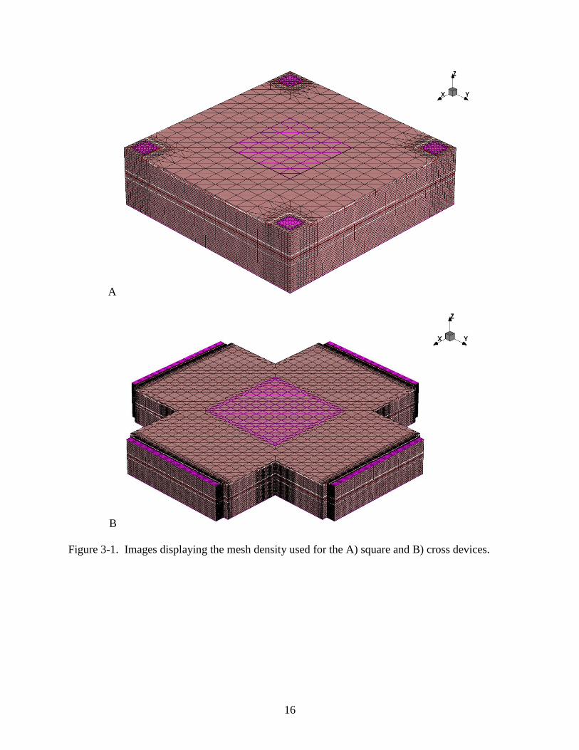
differential calculations from each mesh component. Mesh density is made to be higher near the
contacts of the devices, as shown in Figure 3-1, in order to maximize the model accuracy near
the most volatile regions while maintaining a reasonable runtime. Sentaurus implements
advanced mobility models using these processes, as well as Monte Carlo models for carrier
transport, multiband modeling, carrier temperature and effective mass effects, and so on. The
main Sentaurus feature used for this study is the First Order Kanda model, which models
piezoresistive effects using the mathematics shown previously in Equations 2-1 through 2-5.
In addition to Sentaurus Device, Florida Object Oriented Device Simulator (FLOODS, a
subset of FLOOXS) is used to verify Sentaurus results with the goal of developing an even better
simulation tool. The Scharfetter-Gummel approach utilized by Sentaurus has several drawbacks,
namely its inability to perform mobility modeling with both stress and magnetic field applied
simultaneously, also known as the piezo-Hall effect. FLOOXS uses a finite element approach in
which these effects can be coupled together, which is a goal that is still in development.
16
A
B
Figure 3-1. Images displaying the mesh density used for the A) square and B) cross devices.
17
CHAPTER 4
RESULTS
Resistance Changes Due to Mechanical Stress
As shown in Kanda’s work [1] and in Equation 2-5, the application of compressive stress
along a given crystal axis compresses the crystal lattice in the direction of stress, thereby
increasing majority carrier mobility and decreasing resistance of the device in that direction.
Following Poisson’s ratio [6], this also results in a stretching of the lattice in the perpendicular
crystal directions, leading to a decrease in majority carrier mobility and an increase in resistance
in those directions. Understanding these piezoresistive effects is the key that leads to the
modeling of resistance and offset voltage changes in Hall-effect sensor devices due to
mechanical stress.
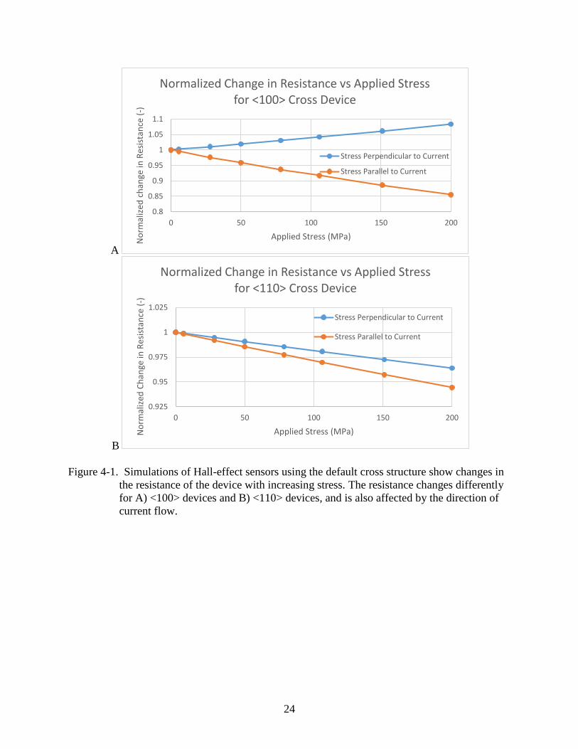
The simplest device with which to view the effect of the relationship between current
direction and stress direction is the original cross structure device (Figure 2-1). With the default
configuration of this device, the direction of current flow between the Force1 and Force2
terminals is directly along the X axis, and the direction of current flow between the Hall1 and
Hall2 terminals is directly along the Y axis. Figure 4-1 shows the change in resistance of devices
with both <100> and <110> crystal orientations. For the <100> device shown in Figure 4-1 A,
the resistance of the device increases by nearly 10% when 200MPa is applied perpendicular to
the current direction, and the resistance of the device decreases by close to 15% when 200MPa is
applied parallel to the current direction. This is consistent with Equation 2-5 relating the
direction of stress and direction of current to a change in resistivity of the device. Figure 4-1 B
shows the results when the same test is run on a <110> device. Since the current and stress are
no longer aligned parallel or perpendicular to the crystal axes, the resistance for both current
directions decrease, but the decrease in the resistance for the parallel case (approximately 6%) is
18
greater than the decrease in the resistance for the perpendicular case (approximately 3.5%). This
is also consistent with the Kanda [1] derivations. Of all of these tests, the resistance change is
maximal when the current and stress are both parallel to one of the crystal axes (the <100> case),
which is supported by the Kanda derivation as well.
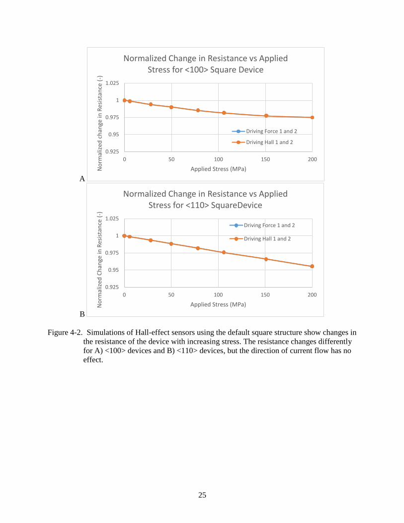
Moving to the square structure tested for the data shown in Figure 4-2, any terminal on
which current is driven results in a 45° angle between the stress direction and the current
direction. Therefore, the resistance changes for all four driving terminals are the same. With
200MPa of stress, this corresponds to a 2.5% change in resistance in the <100> device shown in
Figure 4-2 A, and a nearly 5% resistance change in the <110> device shown in Figure 4-2 B.
To verify that these resistance changes are solely dependent on the direction of current
flow compared to the direction of stress, these results can be compared to the results shown in
Figure 4-3 and Figure 4-4, which show the cross and square structures, respectively, after a 45°
rotation around the Z-axis. Figure 4-3 shows the rotated cross structure, where the direction of
current flow from any driving terminal will now be at a 45° angle to the applied stress on the X-
axis. Due to this change in the angle between stress and current, the rotated cross structure now
displays similar resistance change characteristics to the original square structure in Figure 4-2,
wherein all four driving terminals result in a matching decrease in resistance with the application
of mechanical stress. The <100> device shown in Figure 4-3 A displays a resistance decrease of
approximately 3.5% with 200MPa of applied stress, and the <110> device shown in Figure 4-3 B
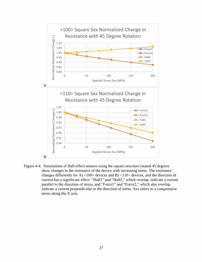
shows a decrease of nearly 5%. Figure 4-4 shows the rotated square structure where the direction
of current flow will be parallel to the compressive stress on the X axis when current is driven
between the “Force1” and “Force2” terminals, and perpendicular to the compressive stress when
current is driven between the “Hall1” and “Hall2” terminals. Similar to the results previously

19
shown for the original cross structure, current driven parallel to the direction of stress results in a
maximally decreasing resistance of approximately 13% for the <100> device shown in Figure 4-
4 A and a decrease of 5.5% for the <110> device shown in Figure 4-4 B. For the case of driving
current perpendicular to stress, the <100> device shown in Figure 4-4 A displays an increase in
resistance of 7% with 200MPa of applied stress and the <110> device in Figure 4-4 B displays a
decrease in resistance of 4%. All of these results are consistent with the mathematics derived in
Equations 2-1 through 2-5.
Offset Voltage Changes Due to Mechanical Stress
The same principles which result in a net decrease in resistance across the device are also
what lead to the creation of an offset voltage across the non-driving terminals of the device
where the voltage created by the presence of a magnetic field would typically be measured. In
the presence of zero magnetic field, mechanical stress can lead to the production of an offset
voltage across these terminals.
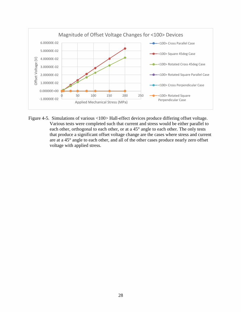
Figure 4-5 shows the magnitude of offset voltage measurements for all configurations of
the <100> device that were tested in this study. The detailed results of each individual
simulation, and those of the similar <110> devices, are described in the upcoming figures. From
Figure 4-5, it is clear to see that the only tests which produced an offset voltage greater than
approximately zero were the original square structure, where stress and current are at a 45° angle
to each other, and the rotated cross structure, where stress and current are also at a 45° angle to
each other.
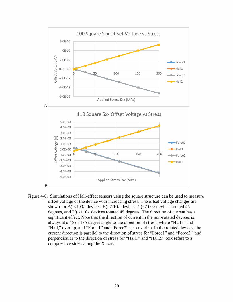
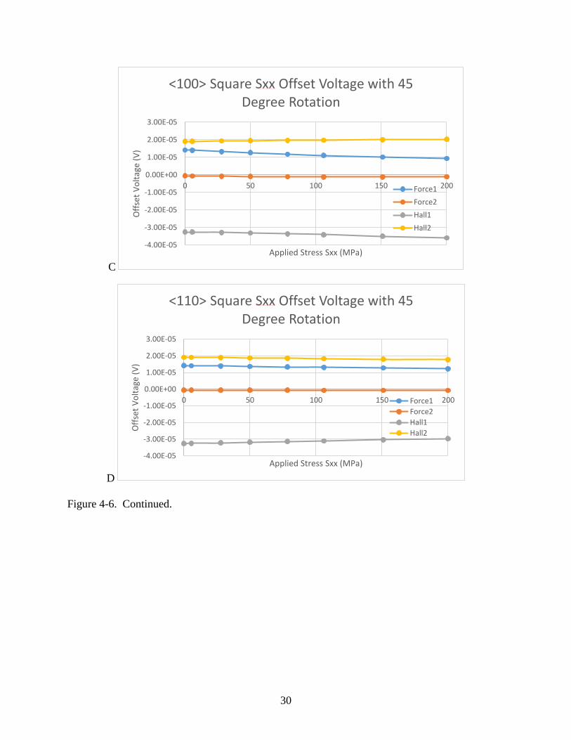
Figure 4-6 shows offset voltage measurements from four configurations of the square
structure. For the <100> and <110> devices in Figure 4-6 A and B, the X-axis compressive stress
is at a 45° angle to the current direction for all four driving terminals. This results in an offset
voltage at 200MPa applied stress of positive or negative 53mV depending on which terminal is

20
measured for the <100> device, and 4.3mV for the <110> device. For the rotated square devices
in Figure 4-6 C and D, the X-axis compressive stress is now parallel to the direction of current
flow when current is driven from the Force1 or Force2 terminals, and perpendicular to the
direction of current flow when current is driven from Hall1 or Hall2. In these cases, the offset
voltage measurements for both the <100> and <110> devices are all in the microvolt range and
do not change with mechanical stress. The small, constant offset can therefore be attributed to
the presence of numerical noise in the calculation, rather than any effect from mechanical stress.
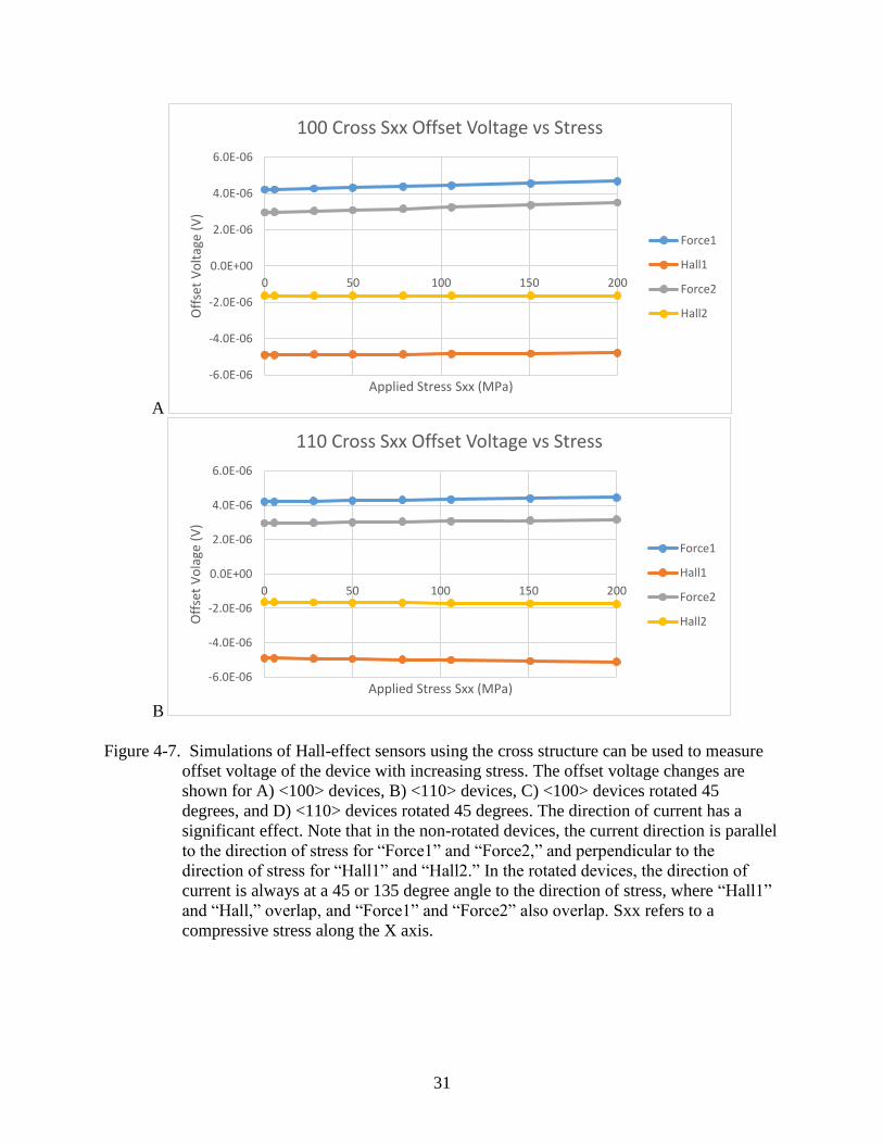
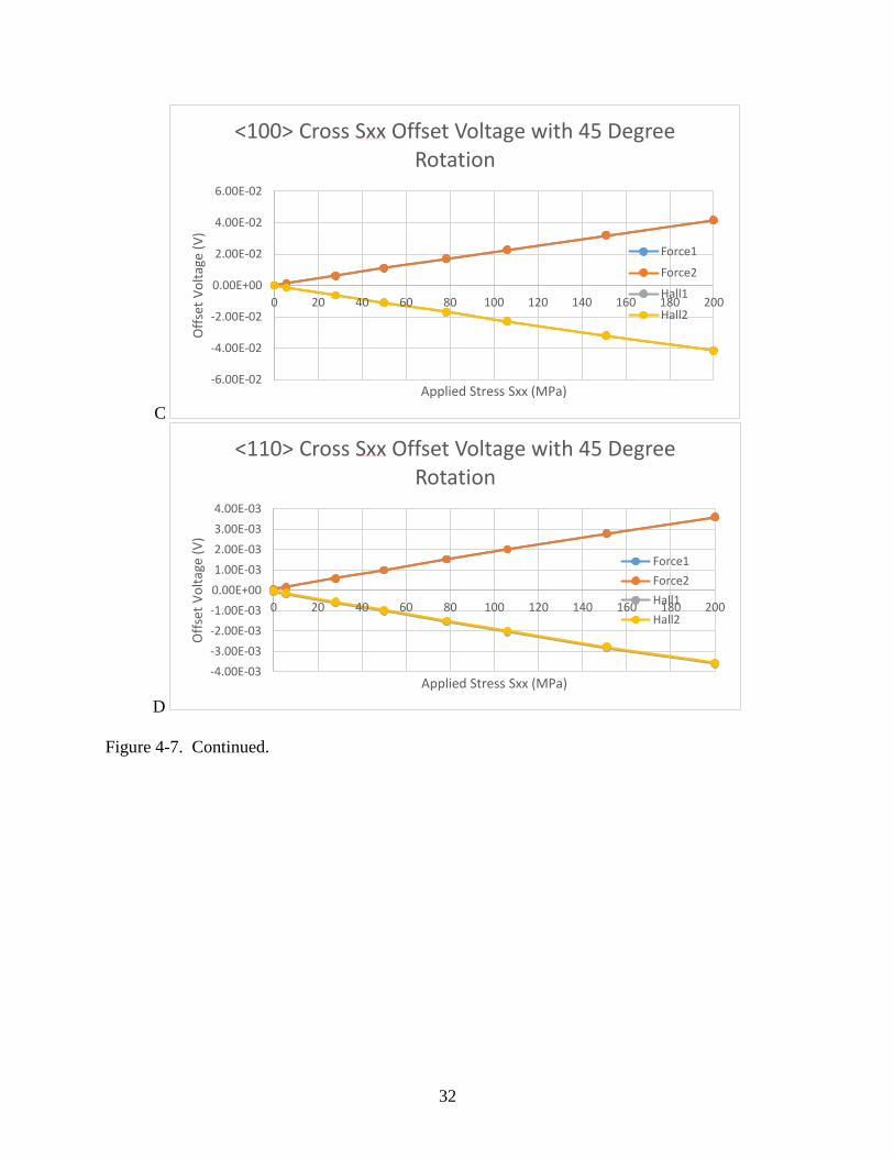
For the cross structure, Figure 4-7 shows the results of offset voltage measurement for
various configurations. In the <100> and <110> devices in their original position, Figure 4-7 A
and B shows that there is no change in offset voltage with stress, and the constant offset voltage
that is measured is in the microvolt range, similar to the rotated square structure. Again, this can
be attributed to numerical noise in the simulation causing the constant offset voltage, and there is
no visible effect of mechanical stress on the offset voltage in this configuration. For the rotated
cross structures, the <100> device in Figure 4-7 C shows an offset voltage change of positive or
negative 40mV depending on the direction of current flow, and the <110> device in Figure 4-7 D
shows an offset voltage change of positive or negative 4mV. This is similar to the change seen in
the original square devices, as in both cases the current direction is always at a 45° angle to the
direction of stress.
Using Electron Mobility and Electrostatic Potential Changes to Understand Trends
To understand how offset voltage forms, Sentaurus simulations can be used to make a
“difference plot” of the stressed case and the non-stressed case. These difference plots are a
valuable tool for visualizing how specific device characteristics can change with increasing
stress. Figure 4-8 shows difference plots between the stressed tests and the zero stress test for the
<100> square device characteristics of electron mobility and electrostatic potential for increasing
21
levels of stress. Figure 4-8 A displays the electron mobility change as stress increases, showing
an increase in electron mobility between the terminals in the vertical direction, which is the
direction of applied stress, as red regions of increasing size and visibility. Horizontally across the
device, perpendicular to the direction of stress, the device shows blue regions which indicate a
decrease in electron mobility in the presence of stress. This change in mobility can be directly
mapped to the electrostatic potential difference plots which are displayed in Figure 4-8 B. The
offset voltage of this device is measured as the electrostatic potential difference between the top
right contact and the bottom right contact. As stress increases, a red region of increased
electrostatic potential appears at the top right terminal, and a blue region of decreased
electrostatic potential appears at the bottom left contact. This net difference maps exactly to the
increased offset voltage displayed in Figure 4-6 A with increasing stress.
To create a summary of the behavior of each device under various current and stress
directions, Figure 4-9, Figure 4-10, Figure 4-11, and Figure 4-12 show difference plots of
electron mobility and electrostatic potential for the <100> square, the <110> square, the <100>
cross, and the <110> cross devices respectively. Each figure displays the difference plots for
electron mobility and electrostatic potential when the current and stress are at 45° angles, when
they are parallel, and when they are perpendicular to each other, all for the maximum stress case
of 200MPa.
In Figure 4-9, the <100> square device displays increasing electron mobility in the
direction of stress for the case of current and stress being at 45° to each other, and a decrease
perpendicular to the direction of stress. This translates directly to the offset voltage seen in the
device for this configuration, as explained above. For the parallel and perpendicular stress and
current directions case, these graphics are a bit more difficult to understand, particularly the
22
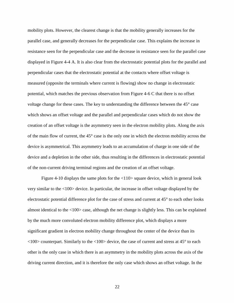
mobility plots. However, the clearest change is that the mobility generally increases for the
parallel case, and generally decreases for the perpendicular case. This explains the increase in
resistance seen for the perpendicular case and the decrease in resistance seen for the parallel case
displayed in Figure 4-4 A. It is also clear from the electrostatic potential plots for the parallel and
perpendicular cases that the electrostatic potential at the contacts where offset voltage is
measured (opposite the terminals where current is flowing) show no change in electrostatic
potential, which matches the previous observation from Figure 4-6 C that there is no offset
voltage change for these cases. The key to understanding the difference between the 45° case
which shows an offset voltage and the parallel and perpendicular cases which do not show the
creation of an offset voltage is the asymmetry seen in the electron mobility plots. Along the axis
of the main flow of current, the 45° case is the only one in which the electron mobility across the
device is asymmetrical. This asymmetry leads to an accumulation of charge in one side of the
device and a depletion in the other side, thus resulting in the differences in electrostatic potential
of the non-current driving terminal regions and the creation of an offset voltage.
Figure 4-10 displays the same plots for the <110> square device, which in general look
very similar to the <100> device. In particular, the increase in offset voltage displayed by the
electrostatic potential difference plot for the case of stress and current at 45° to each other looks
almost identical to the <100> case, although the net change is slightly less. This can be explained
by the much more convoluted electron mobility difference plot, which displays a more
significant gradient in electron mobility change throughout the center of the device than its
<100> counterpart. Similarly to the <100> device, the case of current and stress at 45° to each
other is the only case in which there is an asymmetry in the mobility plots across the axis of the
driving current direction, and it is therefore the only case which shows an offset voltage. In the
23
cases of parallel and perpendicular stress and current directions, the mobility plots are also more
convoluted than their <100> counterparts but show a general trend of increasing electron
mobility throughout the device, with a stronger increase for the parallel case. This is consistent
with the resistance change plots shown in Figure 4-4 B. In a similar fashion to the <100> case,
the electrostatic potential plots for the parallel and perpendicular cases show no change in
electrostatic potential on the contacts which measure offset voltage, matching the lack of offset
voltage change shown in Figure 4-6 D.
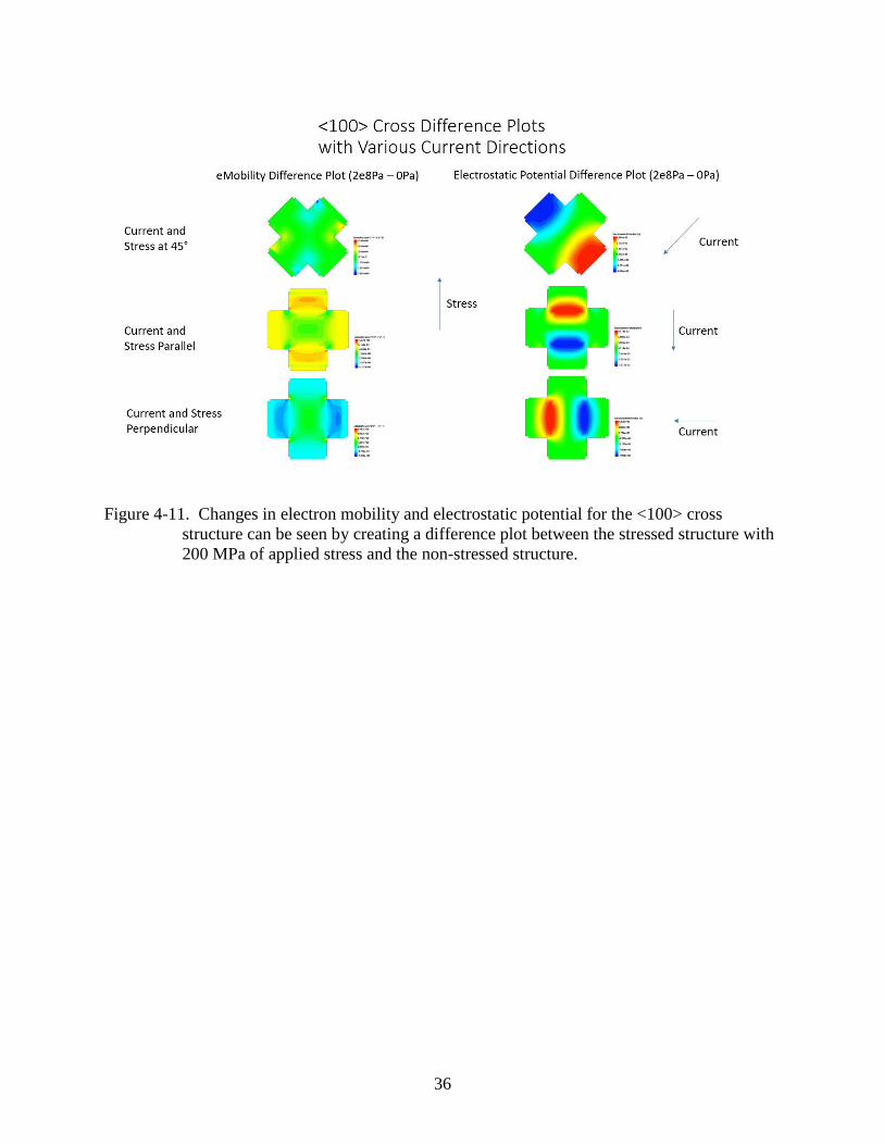
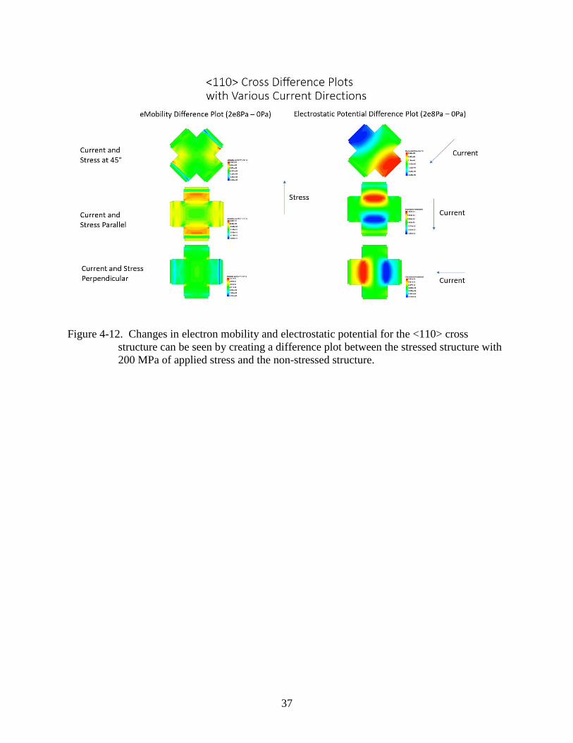
Figures 4-11 and 4-12 show very similar results for the cross structure. Both the <100>
and <110> devices display an offset voltage in the electrostatic potential plots when current is
driven at a 45° angle to the direction of stress. These changes in electrostatic potential can be
explained by small regions of increased mobility in the vertical directions near the current
driving terminals where current flows in the vertical direction towards the offset terminals and
small regions of decreased mobility near the current driving terminals where current flows in the
horizontal direction towards the offset terminals, thus creating an asymmetry in the electron
mobility plots across the axis of the driving current direction. For the parallel and perpendicular
cases, a similar trend in the electron mobility changes can be seen which shows a net decrease in
electron mobility in the <100> parallel case, and a net increase in electron mobility in the <100>
perpendicular case and both <110> cases. This corresponds to the resistance plots shown in
Figure 4-1 and Figure 4-3. In the electrostatic potential plots for the parallel and perpendicular
cases for both the <100> and <110> devices, there is a change in electrostatic potential in the
driving current direction corresponding to the resistance change, but no change in the
electrostatic potential at the offset terminals, matching the plots in Figure 4-7 A and Figure 4-7 B
where no offset voltage occurs with the application of stress.
24
A
B
Figure 4-1. Simulations of Hall-effect sensors using the default cross structure show changes in
the resistance of the device with increasing stress. The resistance changes differently
for A) <100> devices and B) <110> devices, and is also affected by the direction of
current flow.
0.8
0.85
0.9
0.95
1
1.05
1.1
0 50 100 150 200
No
rmal
ized
ch
ange
in R
esis
tan
ce (
-)
Applied Stress (MPa)
Normalized Change in Resistance vs Applied Stress for <100> Cross Device
Stress Perpendicular to Current
Stress Parallel to Current
0.925
0.95
0.975
1
1.025
0 50 100 150 200
No
rmal
ized
Ch
ange
in R
esis
tan
ce (
-)
Applied Stress (MPa)
Normalized Change in Resistance vs Applied Stress for <110> Cross Device
Stress Perpendicular to Current
Stress Parallel to Current
25
A
B
Figure 4-2. Simulations of Hall-effect sensors using the default square structure show changes in
the resistance of the device with increasing stress. The resistance changes differently
for A) <100> devices and B) <110> devices, but the direction of current flow has no
effect.
0.925
0.95
0.975
1
1.025
0 50 100 150 200
No
rmal
ized
ch
ange
in R
esis
tan
ce (
-)
Applied Stress (MPa)
Normalized Change in Resistance vs Applied Stress for <100> Square Device
Driving Force 1 and 2
Driving Hall 1 and 2
0.925
0.95
0.975
1
1.025
0 50 100 150 200
No
rmal
ized
Ch
ange
in R
esis
tan
ce (
-)
Applied Stress (MPa)
Normalized Change in Resistance vs Applied Stress for <110> SquareDevice
Driving Force 1 and 2
Driving Hall 1 and 2

26
A
B
Figure 4-3. Simulations of Hall-effect sensors using the cross structure rotated 45 degrees show
changes in the resistance of the device with increasing stress. The resistance changes
differently for A) <100> devices and B) <110> devices, but the direction of current
flow has no effect. Sxx refers to a compressive stress along the X axis.
0.95
0.96
0.97
0.98
0.99
1.00
1.01
0 50 100 150 200
No
rmal
ized
Res
ista
nce
Ch
ange
(-)
Applied Stress Sxx (MPa)
<100> Cross Sxx Normalized Resistance Change with 45 Degree Rotation
Force1
Force2
Hall1
Hall2
0.94
0.95
0.96
0.97
0.98
0.99
1.00
1.01
0 50 100 150 200
No
rmal
ized
Res
ista
nce
Ch
ange
(-)
Applied Stress Sxx (MPa)
<110> Cross Sxx Normalized Resistance Change with 45 Degree Rotation
Force1
Force2
Hall1
Hall2
27
A
B
Figure 4-4. Simulations of Hall-effect sensors using the square structure rotated 45 degrees
show changes in the resistance of the device with increasing stress. The resistance
changes differently for A) <100> devices and B) <110> devices, and the direction of
current has a significant effect. “Hall1” and “Hall2,” which overlap, indicate a current
parallel to the direction of stress, and “Force1” and “Force2,” which also overlap,
indicate a current perpendicular to the direction of stress. Sxx refers to a compressive
stress along the X axis.
0.80
0.85
0.90
0.95
1.00
1.05
1.10
0 50 100 150 200
No
rmal
ized
Res
ista
nce
Ch
ange
(-)
Applied Stress Sxx (MPa)
<100> Square Sxx Normalized Change in Resistance with 45 Degree Rotation
Force1
Force2
Hall1
Hall2
0.94
0.95
0.96
0.97
0.98
0.99
1.00
1.01
0 50 100 150 200
No
rmal
ized
Res
ista
nce
Ch
ange
(-)
Applied Stress Sxx (MPa)
<110> Square Sxx Normalized Change in Resistance with 45 Degree Rotation
Force1
Force2
Hall1
Hall2
28
Figure 4-5. Simulations of various <100> Hall-effect devices produce differing offset voltage.
Various tests were completed such that current and stress would be either parallel to
each other, orthogonal to each other, or at a 45° angle to each other. The only tests
that produce a significant offset voltage change are the cases where stress and current
are at a 45° angle to each other, and all of the other cases produce nearly zero offset
voltage with applied stress.
-1.00000E-02
0.00000E+00
1.00000E-02
2.00000E-02
3.00000E-02
4.00000E-02
5.00000E-02
6.00000E-02
0 50 100 150 200 250
Off
set
Vo
ltag
e (V
)
Applied Mechanical Stress (MPa)
Magnitude of Offset Voltage Changes for <100> Devices
<100> Cross Parallel Case
<100> Square 45deg Case
<100> Rotated Cross 45deg Case
<100> Rotated Square Parallel Case
<100> Cross Perpendicular Case
<100> Rotated SquarePerpendicular Case
29
A
B
Figure 4-6. Simulations of Hall-effect sensors using the square structure can be used to measure
offset voltage of the device with increasing stress. The offset voltage changes are
shown for A) <100> devices, B) <110> devices, C) <100> devices rotated 45
degrees, and D) <110> devices rotated 45 degrees. The direction of current has a
significant effect. Note that the direction of current in the non-rotated devices is
always at a 45 or 135 degree angle to the direction of stress, where “Hall1” and
“Hall,” overlap, and “Force1” and “Force2” also overlap. In the rotated devices, the
current direction is parallel to the direction of stress for “Force1” and “Force2,” and
perpendicular to the direction of stress for “Hall1” and “Hall2.” Sxx refers to a
compressive stress along the X axis.
-6.0E-02
-4.0E-02
-2.0E-02
0.0E+00
2.0E-02
4.0E-02
6.0E-02
0 50 100 150 200
Off
set
Vo
ltag
e (V
)
Applied Stress Sxx (MPa)
100 Square Sxx Offset Voltage vs Stress
Force1
Hall1
Force2
Hall2
-5.0E-03
-4.0E-03
-3.0E-03
-2.0E-03
-1.0E-03
0.0E+00
1.0E-03
2.0E-03
3.0E-03
4.0E-03
5.0E-03
0 50 100 150 200
Off
set
Vo
ltag
e (V
)
Applied Stress Sxx (MPa)
110 Square Sxx Offset Voltage vs Stress
Force1
Hall1
Force2
Hall2
30
C
D
Figure 4-6. Continued.
-4.00E-05
-3.00E-05
-2.00E-05
-1.00E-05
0.00E+00
1.00E-05
2.00E-05
3.00E-05
0 50 100 150 200
Off
set
Vo
ltag
e (V
)
Applied Stress Sxx (MPa)
<100> Square Sxx Offset Voltage with 45 Degree Rotation
Force1
Force2
Hall1
Hall2
-4.00E-05
-3.00E-05
-2.00E-05
-1.00E-05
0.00E+00
1.00E-05
2.00E-05
3.00E-05
0 50 100 150 200
Off
set
Vo
ltag
e (V
)
Applied Stress Sxx (MPa)
<110> Square Sxx Offset Voltage with 45 Degree Rotation
Force1
Force2
Hall1
Hall2
31
A
B
Figure 4-7. Simulations of Hall-effect sensors using the cross structure can be used to measure
offset voltage of the device with increasing stress. The offset voltage changes are
shown for A) <100> devices, B) <110> devices, C) <100> devices rotated 45
degrees, and D) <110> devices rotated 45 degrees. The direction of current has a
significant effect. Note that in the non-rotated devices, the current direction is parallel
to the direction of stress for “Force1” and “Force2,” and perpendicular to the
direction of stress for “Hall1” and “Hall2.” In the rotated devices, the direction of
current is always at a 45 or 135 degree angle to the direction of stress, where “Hall1”
and “Hall,” overlap, and “Force1” and “Force2” also overlap. Sxx refers to a
compressive stress along the X axis.
-6.0E-06
-4.0E-06
-2.0E-06
0.0E+00
2.0E-06
4.0E-06
6.0E-06
0 50 100 150 200
Off
set
Vo
ltag
e (V
)
Applied Stress Sxx (MPa)
100 Cross Sxx Offset Voltage vs Stress
Force1
Hall1
Force2
Hall2
-6.0E-06
-4.0E-06
-2.0E-06
0.0E+00
2.0E-06
4.0E-06
6.0E-06
0 50 100 150 200
Off
set
Vo
lage
(V
)
Applied Stress Sxx (MPa)
110 Cross Sxx Offset Voltage vs Stress
Force1
Hall1
Force2
Hall2
32
C
D
Figure 4-7. Continued.
-6.00E-02
-4.00E-02
-2.00E-02
0.00E+00
2.00E-02
4.00E-02
6.00E-02
0 20 40 60 80 100 120 140 160 180 200
Off
set
Vo
ltag
e (V
)
Applied Stress Sxx (MPa)
<100> Cross Sxx Offset Voltage with 45 Degree Rotation
Force1
Force2
Hall1
Hall2
-4.00E-03
-3.00E-03
-2.00E-03
-1.00E-03
0.00E+00
1.00E-03
2.00E-03
3.00E-03
4.00E-03
0 20 40 60 80 100 120 140 160 180 200
Off
set
Vo
ltag
e (V
)
Applied Stress Sxx (MPa)
<110> Cross Sxx Offset Voltage with 45 Degree Rotation
Force1
Force2
Hall1
Hall2
33
A
B
Figure 4-8. Changes in A) electron mobility and B) electrostatic potential for the <100> square
structure can be seen by creating a difference plot between the stressed structure and
the non-stressed structure. The gradient of change can be seen at various levels of
applied stress.

34
Figure 4-9. Changes in electron mobility and electrostatic potential for the <100> square
structure can be seen by creating a difference plot between the stressed structure with
200 MPa of applied stress and the non-stressed structure.

35
Figure 4-10. Changes in electron mobility and electrostatic potential for the <110> square
structure can be seen by creating a difference plot between the stressed structure with
200 MPa of applied stress and the non-stressed structure.
36
Figure 4-11. Changes in electron mobility and electrostatic potential for the <100> cross
structure can be seen by creating a difference plot between the stressed structure with
200 MPa of applied stress and the non-stressed structure.
37
Figure 4-12. Changes in electron mobility and electrostatic potential for the <110> cross
structure can be seen by creating a difference plot between the stressed structure with
200 MPa of applied stress and the non-stressed structure.
38
CHAPTER 5
CONCLUSIONS AND FUTURE WORK
Summary of Findings
As shown in both the cross and square structures, compressive mechanical stress in
silicon Hall-effect sensor devices produces a change in electron mobility which varies based on
current direction relative to stress direction. This change in electron mobility can lead to either
increased or decreased resistance in the device depending on current direction. The maximal
decrease in resistance occurs when current and stress are parallel, and a perpendicular
relationship can lead to increased resistance. These mobility effects can also lead to the
appearance of an offset voltage in Hall-effect devices, which can lead to inaccurate
measurements of magnetic field during their application. These findings show how mechanical
stress leads to performance changes, particularly with the creation of offset voltages from
random stresses induced from sources such as device packaging, and can modeled to understand
the creation of offset voltage in devices. This knowledge can potentially be used to develop a
means with which to counteract the effects of mechanical stress.
Future Work
This work has many future applications, considering the possibility of mechanical stress
affecting semiconductor devices of all types. Future progress on the Hall-effect sensor project in
particular will be focused on implementing mobility models affected by mechanical stress in
addition to magnetic field effects to result in a full piezo-Hall mobility model to measure
changes in the magnetic sensitivity of these devices under mechanical stress. Another future
direction is to explore how exactly stresses form from device packaging and how these stresses
can be modeled, avoided, and counteracted.
39
Exploring other devices, these models can be applied to any silicon device due to the
piezoresistive nature of silicon. In addition, other materials and devices such as silicon-
germanium bipolar junction transistors can be explored. In some applications, mechanical stress
can also induce bandgap changes and other effects which can drastically affect device
performance. Understanding the effects of mechanical stresses on semiconductor devices has
proved to be critical in multiple applications, and continuing this study on how to both counteract
and eventually utilize the effects of mechanical stress is an exciting opportunity to explore.

40
LIST OF REFERENCES
[1] Y. Kanda, “A Graphical Representation Of The Piezoresistance Coefficients In Silicon,”
IEEE Trans. Electron Devices, vol. 29, no. 1, pp. 64–70, 1982.
[2] S. Popovic, R, “Hall Effect Devices,” Inst. Phys. Publ. Bristol Philadelphia, p. 426, 2004.
[3] Synopsys Inc., “Sentaurus Device User Guide,” Santa Clara, June, 2006.
[4] D. L. Scharfetter and H. K. Gummel, "Large-signal analysis of a silicon Read diode
oscillator," in IEEE Transactions on Electron Devices, vol. 16, no. 1, pp. 64-77, Jan 1969.
[5] “Measuring Magnetic Fields,” Measuring Mag Fields. [Online]. Available: https://www.nde-
ed.org/EducationResources/CommunityCollege/MagParticle/Physics/Measuring.htm.
[Accessed: 04-Apr-2019].
[6] R. Lakes, “Meaning of Poisson's Ratio,” What is Poisson's ratio? [Online]. Available:
http://silver.neep.wisc.edu/~lakes/PoissonIntro.html. [Accessed: 04-Apr-2019].
41
BIOGRAPHICAL SKETCH
Nathan Miller is a graduating Electrical Engineering student at the University of Florida
with a minor in Mathematics. Nathan has performed internships at GE Aviation and Intel
Corporation and will be returning to Intel Corporation’s Nonvolatile Memory Systems Group
this summer before beginning his PhD studies at Georgia Institute of Technology during the fall
of 2019.
Errata
Simulating the Effects of Mechanical Stress on Hall-Effect Sensor Devices
Undergraduate Thesis
Nathan E. Miller
University of Florida 2019
1. On page 11, line eight, replace “compressive” with “tensile”.
2. On page 17, line two, replace “compressive” with “tensile”.
3. On page 18, third and fourth to last lines, replace “compressive” with “tensile”.
4. On page 19, fourth to last line, replace “compressive” with “tensile”.
5. On page 20, line one, replace “compressive” with “tensile”.
6. On page 21, line seven, replace “bottom right” with “bottom left”.
7. On page 26, last line of Figure 4-3 caption, replace “compressive” with “tensile”.
8. On page 27, second to last line of Figure 4-4 caption, replace “compressive” with
“tensile”.
9. On page 29, second to last line of Figure 4-6 caption, replace “compressive” with
“tensile”.
10. On page 31, second to last line of Figure 4-7 caption, replace “compressive” with
“tensile”.
11. On page 38, first line, replace “compressive” with “tensile”.