Investigation of the Piezoresistive Properties of Nano ...
4
Investigation of the Piezoresistive Properties of Nano Structured Amorphous Carbon for Force Sensor Applications H. Lüthje (1) , S. Biehl (1) , R. Bandorf (1) , J.-H. Sick (1) , E. Peiner (2) , A. Tibrewala (2) (1) Fraunhofer Institute for Surface Engineering and Thin Films, (2) Technical University of Braunschweig. ABSTRACT This paper deals with the preparation and investigation of nano structured diamond-like-carbon films with respect to the piezo resistive, electrical and mechanical properties. Therefore a-C, a-C:H and doped a-C:H:W films were prepared at different plasma conditions.The films were mechanically characterized by AFM and Hysitron, which was also used for nano topographic investigations. Selected films were investigated by Raman spectroscopy for revealing the sp 2 /sp 3 bonding ratio.For investigations of the electrical transport mechanism and the piezoresistive properties the films were deposited on Si-wafer and on steel substrates. The measurements included resistivity vs load, strain and temperature plots. This piezoresistive carbon coating can be used for force/pressure transducer and tribological coating as well. This allows direct measurements at mechanically treated surfaces. Keywords: Amorphous carbon, piezoresistivity, load sensor, sensor washer, intelligent bearing 1 INTRODUCTION Thin Films of amorphous carbon (a-C) and hydrogenated amorphous carbon (a-C:H) have superior tribological properties. They combine high hardness ( up to 60 GPa) and extreme wear resistance with very low friction (μ ~0.1). Moreover they proved to be corrosion resistant and their Young’s Module is in the order of 200 to 300 GPa, which makes them very reliable for various technical applications. An essential advantage is further given by low temperature processing of the films (<120°C) by plasma CVD and PVD. It is well known, that crystalline diamond as the hardest known material exhibits considerable piezo resistive effects, but the high fabrication temperature of >800°C and costs prevent broad industrial uses. In previous papers we reported about the piezo resistivity of amorphous carbon films and their application potential [2,3]. However, knowledge on the piezo resistive mechanism in amorphous carbon films and the influence of nano structure and nano topography on the load/pressure behavior is still lacking. Amorphous carbon is a generic term for hard carbon based layers. We must distinguish between carbon films without hydrogen (a-C; ta-C) and carbon-hydrogen films (DLC, a- CH), which can also be doped with different elements (a:CH:Me). These films in common have carbon bindings in sp 2 and sp 3 states. The sp 3 /sp 2 ratio depends on the growth technique and conditions, hydrogen concentration and doping of the films. 2 EXPERIMENTAL The following chapter deals with the preparation and characterization of a-C:H, a-C:H:W and a-C films. The substrate temperature during deposition was in all cases less than 150 °C. 2.1 Preparation of carbon films Hydrogenated amorphous carbon films (a-C:H) were fabricated by using plasma enhanced chemical vapor deposition (PACVD). As equipment a modified sputter tool (Balzers BAS 450) working at 13,56 MHz was used. Substrates have been polished plates of steel 100Cr6 and Si-wafer. The a-C:H deposition was carried out in a mixture of acetylene and argon. Based on previous process optimizations, the C 2 H 2 flow and the C 2 H 2 /Ar gas-flow ratio were kept constant throughout that investigation. The working pressure was 0.5 Pa. Substrate power (100 – 1000 W) and bias potential at the substrate holder was varied (200V to 800V). Tungsten doped hydrogenated carbon films (a-C:H:W) were deposited on wafers and steel substrates by use of the same plant, but this time deposition was performed by reactive sputtering. To this a tungsten target of 5x10inch was used as magnetron source. The target was driven by a dc-power generator. The process steps were as follows: i) target and substrate etching, ii) sputtering of a thin W adhesion layer in argon, iii) preparation of a gradient layer W:C:H by adding Ethin to the argon gas, iiii) reactive sputtering of a-C:H:W. The W content was varied by adaptation of the Ar:C 2 H 2 gas flow ratio. The pressure was kept constant. Amorphous carbon films (a-C) were deposited by dc magnetron sputtering of a graphite target using a Balzers BAS 450 sputter plant. Process gas was pure argon. DC- Power was kept constant at 1.5 KW. A substrate bias of - 100V was maintained due to previous studies of deposition parameters. 800 NSTI-Nanotech 2006, www.nsti.org, ISBN 0-9767985-6-5 Vol. 1, 2006
Transcript of Investigation of the Piezoresistive Properties of Nano ...

Investigation of the Piezoresistive Properties of Nano Structured Amorphous Carbon for Force Sensor Applications
H. Lüthje(1), S. Biehl (1), R. Bandorf(1), J.-H. Sick(1), E. Peiner(2), A. Tibrewala(2)
(1)Fraunhofer Institute for Surface Engineering and Thin Films, (2)Technical University of Braunschweig.
ABSTRACT
This paper deals with the preparation and investigation of nano structured diamond-like-carbon films with respect to the piezo resistive, electrical and mechanical properties. Therefore a-C, a-C:H and doped a-C:H:W films were prepared at different plasma conditions.The films were mechanically characterized by AFM and Hysitron, which was also used for nano topographic investigations. Selected films were investigated by Raman spectroscopy for revealing the sp2 /sp3 bonding ratio.For investigations of the electrical transport mechanism and the piezoresistive properties the films were deposited on Si-wafer and on steel substrates. The measurements included resistivity vs load, strain and temperature plots. This piezoresistive carbon coating can be used for force/pressure transducer and tribological coating as well. This allows direct measurements at mechanically treated surfaces.
Keywords: Amorphous carbon, piezoresistivity, load sensor, sensor washer, intelligent bearing
1 INTRODUCTION Thin Films of amorphous carbon (a-C) and hydrogenated amorphous carbon (a-C:H) have superior tribological properties. They combine high hardness ( up to 60 GPa) and extreme wear resistance with very low friction (µ ~0.1). Moreover they proved to be corrosion resistant and their Young’s Module is in the order of 200 to 300 GPa, which makes them very reliable for various technical applications. An essential advantage is further given by low temperature processing of the films (<120°C) by plasma CVD and PVD.
It is well known, that crystalline diamond as the hardest known material exhibits considerable piezo resistive effects, but the high fabrication temperature of >800°C and costs prevent broad industrial uses. In previous papers we reported about the piezo resistivity of amorphous carbon films and their application potential [2,3]. However, knowledge on the piezo resistive mechanism in amorphous carbon films and the influence of nano structure and nano topography on the load/pressure behavior is still lacking.
Amorphous carbon is a generic term for hard carbon based layers. We must distinguish between carbon films without hydrogen (a-C; ta-C) and carbon-hydrogen films (DLC, a-CH), which can also be doped with different elements
(a:CH:Me). These films in common have carbon bindings in sp2 and sp3 states. The sp3 /sp2 ratio depends on the growth technique and conditions, hydrogen concentration and doping of the films.
2 EXPERIMENTAL
The following chapter deals with the preparation and characterization of a-C:H, a-C:H:W and a-C films. The substrate temperature during deposition was in all cases less than 150 °C.
2.1 Preparation of carbon films
Hydrogenated amorphous carbon films (a-C:H) were fabricated by using plasma enhanced chemical vapor deposition (PACVD). As equipment a modified sputter tool (Balzers BAS 450) working at 13,56 MHz was used. Substrates have been polished plates of steel 100Cr6 and Si-wafer. The a-C:H deposition was carried out in a mixture of acetylene and argon. Based on previous process optimizations, the C2H2 flow and the C2H2/Ar gas-flow ratio were kept constant throughout that investigation. The working pressure was 0.5 Pa. Substrate power (100 – 1000 W) and bias potential at the substrate holder was varied (200V to 800V).
Tungsten doped hydrogenated carbon films (a-C:H:W) were deposited on wafers and steel substrates by use of the same plant, but this time deposition was performed by reactive sputtering. To this a tungsten target of 5x10inch was used as magnetron source. The target was driven by a dc-power generator. The process steps were as follows: i) target and substrate etching, ii) sputtering of a thin W adhesion layer in argon, iii) preparation of a gradient layer W:C:H by adding Ethin to the argon gas, iiii) reactive sputtering of a-C:H:W. The W content was varied by adaptation of the Ar:C2H2 gas flow ratio. The pressure was kept constant.
Amorphous carbon films (a-C) were deposited by dc magnetron sputtering of a graphite target using a Balzers BAS 450 sputter plant. Process gas was pure argon. DC-Power was kept constant at 1.5 KW. A substrate bias of -100V was maintained due to previous studies of deposition parameters.
800 NSTI-Nanotech 2006, www.nsti.org, ISBN 0-9767985-6-5 Vol. 1, 2006

2.2 Characterization of carbon films
In characterizing amorphous hydrogenated carbon films we first started with SIMS measurements of the hydrogen content in the films. The results are plotted in table 1.
Table 1. Comparison of hydrogen content with bias potential at different depth profiles
Bias-voltage
Hardness GPa
H [at%] 0 – 1,75 µm
thickness
H [at%] 1,75 – 3,5 µm
thickness 200 V 25 24,8 18,7 350 V 22 14,5 15,3 500 V 20 14,5 15,0 650 V 23 14,0 14,2 800 V 25 12,8 13,3
For a-C:H films in figure 1 a plot of roughness and rate of deposition vs bias voltage of a-C:H on Si substrate is shown. The deposition rate increases from 20 nm/min to 36 nm/min upon increasing the bias voltage from -200 to -800 V. Simultaneously, the roughness decreases from 15.6 nm to 8.5 nm. The hardness of the a-C:H films measured using nanoindentation was in between 21-26 GPa, showing a minimum value of 21 GPa at 500 V. The hydrogen content of 12-15 at% does depend on the bias voltage in the range of 350-800 V. A value of 25 at% was observed at 200 V.
AFM-topography measurement of the different films fabricated on polished Si-wafer showed an increased smoothness with bias energy. For 200V and 800V the roughness was 16nm and 8,5nm, respectively.
Fig. 1 Roughness and rate of deposition vs bias voltage of a-C:H on Si
Additional film characterization was performed by means of spectroscopic ellipsometry (VASE) and Raman spectroscopy. The percentage of sp3 bonds was in the range of 24-34%, showing maximum value of 34 % at 350 V.
Fig. 2 TEM-photography of the nano structure of a-C:H films
The mechanical properties of the a-C:H films were measured by means of standard equipment. Nano indentation was used for hardness and elasticity measurement, whereas pin-on disc was used for friction and wear determination. The results can be summarized as follows: The coefficient of friction for Al2O3 counterpart material varied between 0,2 and 0,08 for 400V and 800V bias, respectively. Abrasive wear resistance was very good for all films. Wear for a-C and a-C:H was 150 times lower than wear for hard TiN films.
A trade-off had to be found with respect to the bias voltage selected during the deposition of a-C:H. For strain gauge application defect free films are extremely important since pinholes may deteriorate the electrical properties of vertically connected a-C:H strain gauge resistors. The best results were found at a bias voltage of -350 V. The nano structure of a-C:H films can be seen in Fig. 2. This film was fabricated at the above mentioned parameters.
Tungsten doped a-C:H films showed in contrast to a-C:H layers a different nano structure as shown by the TEM picture in Fig. 3. In this case small crystallites of W can be observed with an average diameter in the order of 5 nm embedded in a matrix of a-C:H. The deposition rate for a-C:H:W layers by use of reactive dc-sputtering was much higher compared to a-C:H and was in the order of 50 -70 nm/h
Fig. 3 TEM–picture of the nano structure of W-doped a-C:H films
801NSTI-Nanotech 2006, www.nsti.org, ISBN 0-9767985-6-5 Vol. 1, 2006

However, hardness for layers with 10-12At% W was lower than a-C:H hardness and resulted to ~15 GPa and friction was about 0,2.
For a-C films very high hardness values of 50 GPa were obtained. Hardness in the range of some ten GPa can be expected for sputtered amorphous carbon with a content of tetrahedral-bonded carbon (sp3) of around 25% [1]. The coefficient of friction was <0,1. AFM measurement of the nano roughness of sputtered a-C films showed very low roughness in the order of Ra~0,5 nm. The hydrogen content in the films determined by secondary ion mass spectroscopy (SIMS) was less than 2%. More details on the a-C deposition process and the tribological testing were reported elsewhere [2].
3 ELECTRICAL CHARACTERIZATION
The electrical resistivity of the carbon films discussed in this paper was different. Whereas a-C and doped a-CH:W films typically showed rather low electrical resistivities in the range of mΩcm to some kΩcm, a-C:H films are in the order of MΩcm.
A typical current-voltage characteristic measured at room temperature on a test structure without applying force on it is shown in figure 5. It is almost linear between ± 1 V, followed by a deviation from linearity towards higher current. Polarity of voltage and direction of current across the a-C:H heterojunction are given in the inset. Above 1 V a linear relationship is observed in figure 5b as expected for the Schottky and for Frenkel-Poole carrier emission mechanisms which can control conduction across heterojunctions on silicon. In addition, we measured I-V characteristics of a-C:H in the temperature range of 30-150 °C. Ohmic behaviour followed by Frenkel-Poole conduction at higher voltages was found correspondingly. A typical Arrhenius plot of conductivity measured in the linear range of the I-V characteristics resulting in an activation energy of Ea=0.48 eV, which is comparable to values reported for tetrahedral amorphous carbon (ta-C) films (0.45 eV).
Fig. 5 Typical current-voltage characteristic of a-C:H
Fig. 6 Current-voltage characteristic of a-C film. For I-V measurement a meander-like structure of 250 nm a-C thickness was prepared on oxidized Si.
3.1 Piezoresistive Investigations
The standard measurement of the piezoresistive k-factor will be performed by use of substrate bending methods. However, for films with low conductivity special procedures which allow resistivity measurements at narrow distances of stressed films had to be developed.
For solving that problem, we make use of micro mechanical techniques and prepared the a-C:H film to be investigated on a special designed Si-membrane. The arrangement in principle was based on a thin doped Si-membrane carrying in the centre an unthinned part (boss) for introducing the load. As demonstrated in fig.7 the a-C:H coating was only locally applied by use of lift-off masking. Top electrode and wiring was performed by photolithography.
Fig. 7 Schematic drawing for illustration of the measurement of the a-C:H force sensors under strain introduction by lateral elongation and compression
By use oft his method we obtained k-factors of 60 for our a-C films and 90 for a-C:H films. Arrhenious behavior is observed for the resistivity of a-C:H with respect to temperature. The K is independent of temperature in the range of 23-60 °C.
a-C
802 NSTI-Nanotech 2006, www.nsti.org, ISBN 0-9767985-6-5 Vol. 1, 2006
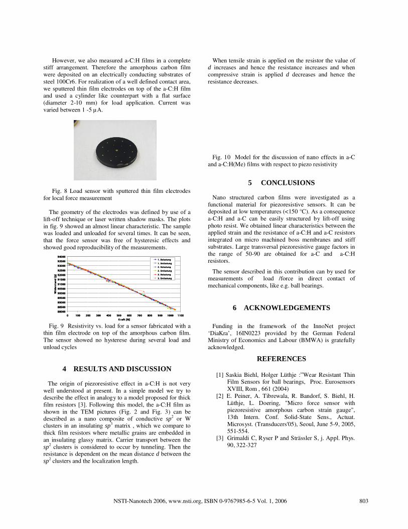
However, we also measured a-C:H films in a complete stiff arrangement. Therefore the amorphous carbon film were deposited on an electrically conducting substrates of steel 100Cr6. For realization of a well defined contact area, we sputtered thin film electrodes on top of the a-C:H film and used a cylinder like counterpart with a flat surface (diameter 2-10 mm) for load application. Current was varied between 1 -5 µA.
Fig. 8 Load sensor with sputtered thin film electrodes for local force measurement
The geometry of the electrodes was defined by use of a lift-off technique or laser written shadow masks. The plots in fig. 9 showed an almost linear characteristic. The sample was loaded and unloaded for several times. It can be seen, that the force sensor was free of hysteresic effects and showed good reproducibility of the measurements.
88000880008800088000
88500885008850088500
89000890008900089000
89500895008950089500
90000900009000090000
90500905009050090500
91000910009100091000
91500915009150091500
92000920009200092000
92500925009250092500
93000930009300093000
93500935009350093500
94000940009400094000
0000 100100100100 200200200200 300300300300 400400400400 500500500500 600600600600 700700700700 800800800800 900900900900 1000100010001000 1100110011001100
Kraft [N]Kraft [N]Kraft [N]Kraft [N]
Wid
ers
tan
d [
W
ide
rsta
nd
[
Wid
ers
tan
d [
W
ide
rsta
nd
[ ΩΩ ΩΩ]] ]]
1 . Belastung1. Belastung1. Belastung1. Belastung
1. Entlastung1. Entlastung1. Entlastung1. Entlastung
2. Belastung2. Belastung2. Belastung2. Belastung
2. Entlastung2. Entlastung2. Entlastung2. Entlastung
3. Belastung3. Belastung3. Belastung3. Belastung
3. Entlastung3. Entlastung3. Entlastung3. Entlastung
Fig. 9 Resistivity vs. load for a sensor fabricated with a thin film electrode on top of the amorphous carbon film. The sensor showed no hysterese during several load and unload cycles
4 RESULTS AND DISCUSSION
The origin of piezoresistive effect in a-C:H is not very well understood at present. In a simple model we try to describe the effect in analogy to a model proposed for thick film resistors [3]. Following this model, the a-C:H film as shown in the TEM pictures (Fig. 2 and Fig. 3) can be described as a nano composite of conductive sp2 or W clusters in an insulating sp3 matrix , which we compare to thick film resistors where metallic grains are embedded in an insulating glassy matrix. Carrier transport between the sp2 clusters is considered to occur by tunneling. Then the resistance is dependent on the mean distance d between the sp2 clusters and the localization length.
When tensile strain is applied on the resistor the value of d increases and hence the resistance increases and when compressive strain is applied d decreases and hence the resistance decreases.
Fig. 10 Model for the discussion of nano effects in a-C and a-C:H(Me) films with respect to piezo resistivity
5 CONCLUSIONS
Nano structured carbon films were investigated as a functional material for piezoresistive sensors. It can be deposited at low temperatures (<150 °C). As a consequence a-C:H and a-C can be easily structured by lift-off using photo resist. We obtained linear characteristics between the applied strain and the resistance of a-C:H and a-C resistors integrated on micro machined boss membranes and stiff substrates. Large transversal piezoresistive gauge factors in the range of 50-90 are obtained for a-C and a-C:H resistors.
The sensor described in this contribution can by used for measurements of load /force in direct contact of mechanical components, like e.g. ball bearings.
6 ACKNOWLEDGEMENTS
Funding in the framework of the InnoNet project ‘DiaKra’, 16IN0223 provided by the German Federal Ministry of Economics and Labour (BMWA) is gratefully acknowledged.
REFERENCES
[1] Saskia Biehl, Holger Lüthje :”Wear Resistant Thin Film Sensors for ball bearings, Proc. Eurosensors XVIII, Rom , 661 (2004)
[2] E. Peiner, A. Tibrewala, R. Bandorf, S. Biehl, H. Lüthje, L. Doering, "Micro force sensor with piezoresistive amorphous carbon strain gauge", 13th Intern. Conf. Solid-State Sens., Actuat. Microsyst. (Transducers'05), Seoul, June 5-9, 2005, 551-554.
[3] Grimaldi C, Ryser P and Strässler S, j. Appl. Phys. 90, 322-327
803NSTI-Nanotech 2006, www.nsti.org, ISBN 0-9767985-6-5 Vol. 1, 2006