Piezoresistive Pressure Sensor
24
This model is licensed under the COMSOL Software License Agreement 5.6. All trademarks are the property of their respective owners. See www.comsol.com/trademarks. Created in COMSOL Multiphysics 5.6 Piezoresistive Pressure Sensor
Transcript of Piezoresistive Pressure Sensor

Created in COMSOL Multiphysics 5.6
P i e z o r e s i s t i v e P r e s s u r e S e n s o r
This model is licensed under the COMSOL Software License Agreement 5.6.All trademarks are the property of their respective owners. See www.comsol.com/trademarks.
Introduction
Piezoresistive pressure sensors were some of the first MEMS devices to be commercialized. Compared to capacitive pressure sensors, they are simpler to integrate with electronics, their response is more linear, and they are inherently shielded from RF noise. They do, however, usually require more power during operation, and the fundamental noise limits of the sensor are higher than their capacitive counterparts. Historically, piezoresistive devices have been dominant in the pressure sensor market.
This example considers the design of the MPX100 series pressure sensors originally produced by the semiconductor products division of Motorola Inc. (now Freescale Semiconductor Inc.). Although the sensor is no longer in production, a detailed analysis of its design is given in Ref. 1, and an archived data sheet is available from Freescale Semiconductor Inc. (Ref. 2).
Model Definition
The model consists square membrane with side 1 mm and thickness 20 μm, supported around its edges by region 0.1mm wide, which is intended to represent the remainder of the wafer. The supporting region is fixed on its underside (representing a connection to the thicker handle of the device die). Near to one edge of the membrane an X-shaped piezoresistor (or Xducer™)1 and part of its associated interconnects are visible. The geometry is shown in Figure 1.
The piezoresistor is assumed to have a uniform p-type dopant density of 1.32×1019 cm−3 and a thickness of 400 nm. The interconnects are assumed to have the same thickness but a dopant density of 1.45×1020 cm−3. Only a part of the interconnects is included in the geometry, since their conductivity is sufficiently high that they do not contribute to the voltage output of the device (in practice the interconnects would also be thicker in addition to having a higher conductivity but this also has little effect on the solution).
The edges of the die are aligned with the {110} directions of the silicon. The die edges are also aligned with the global X and Y axes in the COMSOL Multiphysics model. The piezoresistor is oriented at 45 to the die edge, and so lies in the [100] direction of the
1. Xducer™ is believed to be a trademark of Freescale Semiconductor, Inc. f/k/a Motorola, Inc. NeitherFreescale Semiconductor Inc. nor Motorola, Inc. has in any way provided any sponsorship or endorsement of, nordo they have any connection or involvement with, COMSOL Multiphysics® software or this model.
2 | P I E Z O R E S I S T I V E P R E S S U R E S E N S O R

crystal. In the COMSOL Multiphysics model, a coordinate system rotated 45 about the global Z-axis is added to define the orientation of the crystal.
Figure 1: Left: Model geometry. Right: Detail showing the piezoresistor geometry.
D E V I C E P H Y S I C S A N D E Q U A T I O N S
The conductivity of the Xducer™ sensor changes when the membrane in its vicinity is subject to an applied stress. This effect is known as the piezoresistance effect and is usually associated with semiconducting materials. In semiconductors, piezoresistance results from the strain-induced alteration of the material’s band structure, and the associated changes in carrier mobility and number density. The relation between the electric field, E, and the current, J, within a piezoresistor is:
(1)
where ρ is the resistivity and Δρ is the induced change in the resistivity. In the general case both ρ and Δρ are rank 2 tensors (matrices). The change in resistance is related to the stress, σ, by the constitutive relationship:
(2)
where Π is the piezoresistance tensor (SI units: Pa−1Ωm), a material property. Note that the definition of Π in COMSOL Multiphysics includes the resistivity in each element of the tensor, rather than having a scalar multiple outside of Π (which is possible only for materials with isotropic conductivity). Π is in this case a rank-4 tensor; however, it can be represented as a matrix if the resistivity and stress are converted to vectors within a reduced subscript notation. Within the Voigt notation used by COMSOL Multiphysics for this purpose, Equation 2 becomes:
E ρ J⋅ Δρ J⋅+=
Δρ Π σ⋅=
3 | P I E Z O R E S I S T I V E P R E S S U R E S E N S O R
(3)
The Δρ vector computed from Equation 3 is assembled into matrix form in the following manner in Equation 1:
(4)
Silicon has cubic symmetry, and as a result the Π matrix can be described in terms of three independent constants in the following manner:
For p-type silicon the Π44 constant is two orders of magnitude larger than either the Π11 or the Π12 coefficients. The Π66 element (which is equal in magnitude to the Π44 element) couples the σxy shear stress, with the Δρxy off-diagonal term in the change in resistivity matrix. In turn, Δρxy couples a current in the x-direction to an induced electric field in the y-direction (and vice versa). This is the principle of the Xducer™ transducer. An applied voltage (typically 3 V; see Ref. 2) across the [100] orientated arm of the X produces a current (typically 6 mA; see Ref. 2) down this arm. Shear stresses are present in the Xducer™ as a result of the pressure induced deformation of the diaphragm in which it is implanted. Through the piezoresistance effect, these shear stresses cause an electric field or potential gradient transverse to the direction of current flow, in the [010] arm of the X.
Δρxx
Δρyy
Δρzz
Δρyz
Δρxz
Δρxy
Π11 Π12 Π13 Π14 Π15 Π16
Π21 Π22 Π23 Π24 Π25 Π26
Π31 Π32 Π33 Π34 Π35 Π36
Π41 Π42 Π43 Π44 Π45 Π46
Π51 Π52 Π53 Π54 Π55 Π56
Π61 Π62 Π63 Π64 Π65 Π66
σ xx
σ yy
σ zz
σ yz
σ xz
σ xy
⋅=
Ex
Ey
Ez
ρxx ρxy ρxz
ρxy ρyy ρyz
ρxz ρyz ρzz
Jx
Jy
Jz
⋅
Δρxx Δρxy Δρxz
Δρxy Δρyy Δρyz
Δρxz Δρyz Δρzz
Jx
Jy
Jz
⋅+=
Π
Π11 Π12 Π12 0 0 0
Π12 Π22 Π12 0 0 0
Π12 Π12 Π33 0 0 0
0 0 0 Π44 0 0
0 0 0 0 Π44 0
0 0 0 0 0 Π44
=
4 | P I E Z O R E S I S T I V E P R E S S U R E S E N S O R
Across the width of the transducer, the potential gradient sums up to produce an induced voltage difference between the [010] arms of the X. According to the device data sheet, under normal operating conditions a 60 mV potential difference is generated from a 100 kPa applied pressure with a 3 V applied bias (Ref. 2).
The situation is complicated somewhat by the detailed current distribution within the device, since the voltage sensing elements increase the width of the current carrying silicon wire locally, leading to a “short circuit” effect (Ref. 3) or a spreading out of the current into the sense arms of the X.
The Piezoresistivity interfaces available in the MEMS Module solve Equation 3 and an inverse form of Equation 4, together with the equations of structural mechanics. In this model the Piezoresistivity, Boundary Currents interface is used to model the structural equations on the domain level and to solve the electrical equations on a thin layer coincident with a boundary in the model geometry.
Results and Discussion
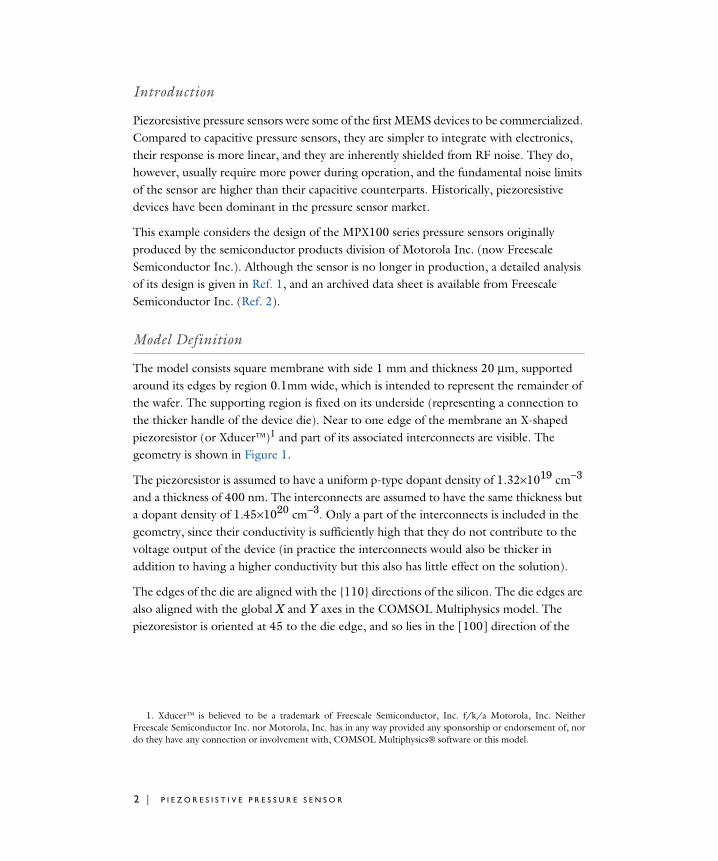
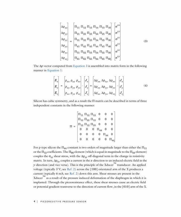
Figure 2 shows the displacement of the diaphragm as a result of a 100 kPa pressure difference. At the center of the diaphragm the displacement is 1.2 μm. A simple isotropic model for the deform displacement given in Ref. 1 predicts an order of magnitude value of 4 μm (assuming a Young’s modulus of 170 GPa and a Poisson’s ratio of 0.06). The agreement is reasonable considering the limitations of the analytic model, which is derived by a crude variational guess. A more accurate value for the shear stress in local coordinates at the midpoint of the diaphragm edge is given in Ref. 1 as:
where P is the applied pressure, L is the length of the diaphragm edge, and H is the diaphragm thickness. This equation predicts the magnitude of the local shear stress to be 35 MPa, in good agreement with the minimum value shown in Figure 3, which is also 35 MPa. Theoretically the shear stress should be maximal at the midpoint of the edge of the diaphragm. Figure 4 shows the shear stress along the edge in the model. This shows a maximum magnitude at the center of each of the two edges along which the plot is made, but the value of this maximum is less than the maximum stress in the model, in part due to the boundary conditions employed on the three dimensional diaphragm. The model:
σl 12, 0.141 LH----- 2
P=
5 | P I E Z O R E S I S T I V E P R E S S U R E S E N S O R
piezoresistive_pressure_sensor_shell.mph shows better agreement with the theoretical maximum shear stress along this edge.
Figure 2: Diaphragm displacement as a result of a 100 kPa applied pressure.
Figure 3: Shear stress, shown in the local coordinate system of the piezoresistor (rotated 45° about the z-axis of the global system). The shear stress is has its highest magnitude close to the piezoresistor with a value of approximately -35 MPa.
6 | P I E Z O R E S I S T I V E P R E S S U R E S E N S O R
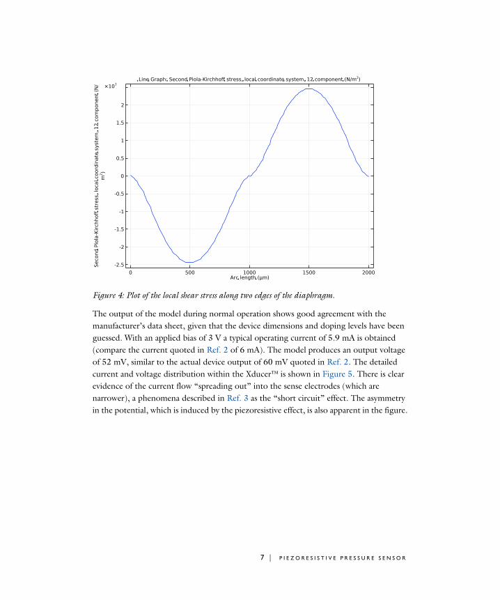
Figure 4: Plot of the local shear stress along two edges of the diaphragm.
The output of the model during normal operation shows good agreement with the manufacturer’s data sheet, given that the device dimensions and doping levels have been guessed. With an applied bias of 3 V a typical operating current of 5.9 mA is obtained (compare the current quoted in Ref. 2 of 6 mA). The model produces an output voltage of 52 mV, similar to the actual device output of 60 mV quoted in Ref. 2. The detailed current and voltage distribution within the Xducer™ is shown in Figure 5. There is clear evidence of the current flow “spreading out” into the sense electrodes (which are narrower), a phenomena described in Ref. 3 as the “short circuit” effect. The asymmetry in the potential, which is induced by the piezoresistive effect, is also apparent in the figure.
7 | P I E Z O R E S I S T I V E P R E S S U R E S E N S O R

Figure 5: Arrows: Current density, Contours: Electric Potential, for a device driven by a 3 V bias with an applied pressure of 100 kPa.
References
1. S.D. Senturia, “A Piezoresistive Pressure Sensor,” Microsystem Design, chapter 18, Springer, 2000.
2. Motorola Semiconductor MPX100 series technical data, document: MPX100/D, 1998 (available from Freescale Semiconductor Inc at http://www.freescale.com).
3. M. Bao, Analysis and Design Principles of MEMS Devices, Elsevier B. V., 2005.
Application Library path: MEMS_Module/Sensors/piezoresistive_pressure_sensor
Modeling Instructions
From the File menu, choose New.
8 | P I E Z O R E S I S T I V E P R E S S U R E S E N S O R

N E W
In the New window, click Model Wizard.
M O D E L W I Z A R D
1 In the Model Wizard window, click 3D.
2 In the Select Physics tree, select Structural Mechanics>Electromagnetics-
Structure Interaction>Piezoresistivity>Piezoresistivity, Boundary Currents.
3 Click Add.
4 Click Study.
5 In the Select Study tree, select General Studies>Stationary.
6 Click Done.
G E O M E T R Y 1
1 In the Model Builder window, under Component 1 (comp1) click Geometry 1.
2 In the Settings window for Geometry, locate the Units section.
3 From the Length unit list, choose µm.
For convenience, the device geometry is inserted from an existing file. You can read the instructions for creating the geometry in the Appendix — Geometry Modeling Instructions.
4 In the Geometry toolbar, click Insert Sequence.
5 Browse to the model’s Application Libraries folder and double-click the file piezoresistive_pressure_sensor_geom_sequence.mph.
6 In the Geometry toolbar, click Build All.
D E F I N I T I O N S
Piezoresistor1 In the Definitions toolbar, click Explicit.
2 In the Settings window for Explicit, type Piezoresistor in the Label text field.
3 Locate the Input Entities section. From the Geometric entity level list, choose Boundary.
4 Select Boundary 46 only.
Connections1 In the Definitions toolbar, click Explicit.
2 In the Settings window for Explicit, type Connections in the Label text field.
3 Locate the Input Entities section. From the Geometric entity level list, choose Boundary.
9 | P I E Z O R E S I S T I V E P R E S S U R E S E N S O R

4 Select Boundaries 14, 22, 26, 39, 46, 73, 77, 81, and 104 only.
Membrane (Lower Surface)1 In the Definitions toolbar, click Box.
2 In the Settings window for Box, type Membrane (Lower Surface) in the Label text field.
3 Locate the Geometric Entity Level section. From the Level list, choose Boundary.
4 Locate the Box Limits section. In the x minimum text field, type -501.
5 In the x maximum text field, type 501.
6 In the y minimum text field, type -30.
7 In the y maximum text field, type 1000.
8 In the z maximum text field, type -1.
9 Locate the Output Entities section. From the Include entity if list, choose Entity inside box.
Membrane (Upper Surface)1 Right-click Membrane (Lower Surface) and choose Duplicate.
2 In the Settings window for Box, type Membrane (Upper Surface) in the Label text field.
3 Locate the Box Limits section. In the z minimum text field, type -1.
4 In the z maximum text field, type inf.
Lower Surface1 In the Definitions toolbar, click Box.
2 In the Settings window for Box, type Lower Surface in the Label text field.
3 Locate the Geometric Entity Level section. From the Level list, choose Boundary.
4 Locate the Box Limits section. In the z maximum text field, type -1.
5 Locate the Output Entities section. From the Include entity if list, choose Entity inside box.
Upper Surface1 Right-click Lower Surface and choose Duplicate.
2 In the Settings window for Box, type Upper Surface in the Label text field.
3 Locate the Box Limits section. In the z minimum text field, type -1.
4 In the z maximum text field, type inf.
10 | P I E Z O R E S I S T I V E P R E S S U R E S E N S O R

Fixed1 In the Definitions toolbar, click Difference.
2 In the Settings window for Difference, type Fixed in the Label text field.
3 Locate the Geometric Entity Level section. From the Level list, choose Boundary.
4 Locate the Input Entities section. Under Selections to add, click Add.
5 In the Add dialog box, select Lower Surface in the Selections to add list.
6 Click OK.
7 In the Settings window for Difference, locate the Input Entities section.
8 Under Selections to subtract, click Add.
9 In the Add dialog box, select Membrane (Lower Surface) in the Selections to subtract list.
10 Click OK.
Electric Currents1 In the Definitions toolbar, click Union.
2 In the Settings window for Union, type Electric Currents in the Label text field.
3 Locate the Geometric Entity Level section. From the Level list, choose Boundary.
4 Locate the Input Entities section. Under Selections to add, click Add.
5 In the Add dialog box, in the Selections to add list, choose Piezoresistor and Connections.
6 Click OK.
Rotated System 2 (sys2)1 In the Definitions toolbar, click Coordinate Systems and choose Rotated System.
2 In the Settings window for Rotated System, locate the Rotation section.
3 Find the Euler angles (Z-X-Z) subsection. In the α text field, type -45[deg].
A D D M A T E R I A L
1 In the Home toolbar, click Add Material to open the Add Material window.
2 Go to the Add Material window.
3 In the tree, select Piezoresistivity>n-Silicon (single-crystal, lightly doped).
4 Click Add to Component 1 (comp1).
5 In the tree, select Piezoresistivity>p-Silicon (single-crystal, lightly doped).
6 Click Add to Component 1 (comp1).
7 In the Home toolbar, click Add Material to close the Add Material window.
11 | P I E Z O R E S I S T I V E P R E S S U R E S E N S O R

M A T E R I A L S
p-Silicon (single-crystal, lightly doped) (mat2)1 In the Settings window for Material, locate the Geometric Entity Selection section.
2 From the Geometric entity level list, choose Boundary.
3 From the Selection list, choose Electric Currents.
S O L I D M E C H A N I C S ( S O L I D )
Linear Elastic Material 11 In the Model Builder window, under Component 1 (comp1)>Solid Mechanics (solid) click
Linear Elastic Material 1.
2 In the Settings window for Linear Elastic Material, locate the Coordinate System Selection section.
3 From the Coordinate system list, choose Rotated System 2 (sys2).
4 Locate the Linear Elastic Material section. From the Solid model list, choose Anisotropic.
5 From the Material data ordering list, choose Voigt (11, 22, 33, 23, 13, 12).
Fixed Constraint 11 In the Physics toolbar, click Boundaries and choose Fixed Constraint.
2 In the Settings window for Fixed Constraint, locate the Boundary Selection section.
3 From the Selection list, choose Fixed.
Boundary Load 11 In the Physics toolbar, click Boundaries and choose Boundary Load.
2 In the Settings window for Boundary Load, locate the Boundary Selection section.
3 From the Selection list, choose Membrane (Upper Surface).
4 Locate the Force section. From the Load type list, choose Pressure.
5 In the p text field, type 100[kPa].
E L E C T R I C C U R R E N T S , S I N G L E L A Y E R S H E L L ( E C S )
1 In the Model Builder window, under Component 1 (comp1) click Electric Currents,
Single Layer Shell (ecs).
2 In the Settings window for Electric Currents, Single Layer Shell, locate the Boundary Selection section.
3 From the Selection list, choose Electric Currents.
4 Locate the Shell Thickness section. In the ds text field, type 400[nm].
12 | P I E Z O R E S I S T I V E P R E S S U R E S E N S O R

5 Click the Show More Options button in the Model Builder toolbar.
6 In the Show More Options dialog box, in the tree, select the check box for the node Physics>Advanced Physics Options.
7 Click OK.
Current Conservation 11 In the Model Builder window, under Component 1 (comp1)>Electric Currents,
Single Layer Shell (ecs) click Current Conservation 1.
2 In the Settings window for Current Conservation, locate the Model Inputs section.
3 In the nd text field, type 1.45e20[1/cm^3].
4 Locate the Coordinate System Selection section. From the Coordinate system list, choose Rotated System 2 (sys2).
Piezoresistive Material 11 In the Model Builder window, click Piezoresistive Material 1.
2 In the Settings window for Piezoresistive Material, locate the Boundary Selection section.
3 From the Selection list, choose Piezoresistor.
4 Locate the Model Input section. In the nd text field, type 1.32e19[1/cm^3].
5 Locate the Coordinate System Selection section. From the Coordinate system list, choose Rotated System 2 (sys2).
Ground 11 In the Physics toolbar, click Edges and choose Ground.
2 Select Edge 195 only.
Terminal 11 In the Physics toolbar, click Edges and choose Terminal.
2 Select Edges 30 and 35 only.
3 In the Settings window for Terminal, locate the Terminal section.
4 From the Terminal type list, choose Voltage.
5 In the V0 text field, type 3.
Terminal 21 In the Physics toolbar, click Edges and choose Terminal.
2 Select Edge 20 only.
Terminal 31 In the Physics toolbar, click Edges and choose Terminal.
13 | P I E Z O R E S I S T I V E P R E S S U R E S E N S O R

2 Select Edges 201 and 205 only.
M E S H 1
1 In the Model Builder window, under Component 1 (comp1) click Mesh 1.
2 In the Settings window for Mesh, locate the Mesh Settings section.
3 From the Sequence type list, choose User-controlled mesh.
Size1 In the Model Builder window, under Component 1 (comp1)>Mesh 1 click Size.
2 In the Settings window for Size, locate the Element Size section.
3 Click the Custom button.
4 Locate the Element Size Parameters section. In the Maximum element size text field, type 60.
5 In the Minimum element size text field, type 0.5.
Size 11 In the Model Builder window, right-click Mesh 1 and choose Size.
2 In the Settings window for Size, locate the Geometric Entity Selection section.
3 From the Geometric entity level list, choose Boundary.
4 From the Selection list, choose Piezoresistor.
5 Locate the Element Size section. Click the Custom button.
6 Locate the Element Size Parameters section. Select the Maximum element size check box.
7 In the associated text field, type 2.
8 Select the Minimum element size check box.
9 In the associated text field, type 0.1.
Size 21 Right-click Size 1 and choose Duplicate.
2 In the Settings window for Size, locate the Geometric Entity Selection section.
3 From the Selection list, choose Connections.
4 Locate the Element Size Parameters section. In the Maximum element size text field, type 6.
Size 31 Right-click Size 2 and choose Duplicate.
2 In the Settings window for Size, locate the Geometric Entity Selection section.
14 | P I E Z O R E S I S T I V E P R E S S U R E S E N S O R

3 From the Geometric entity level list, choose Edge.
4 Select Edges 74, 79, 104, 108, 111, 114, 117, 120, 123, 142, 143, and 146 only.
5 Locate the Element Size Parameters section. In the Maximum element size text field, type 0.4.
Free Tetrahedral 1In the Model Builder window, right-click Free Tetrahedral 1 and choose Disable.
Free Triangular 11 In the Mesh toolbar, click Boundary and choose Free Triangular.
2 In the Settings window for Free Triangular, locate the Boundary Selection section.
3 From the Selection list, choose Upper Surface.
Swept 11 In the Mesh toolbar, click Swept.
2 Click Build Mesh.
3 In the Home toolbar, click Compute.
R E S U L T S
Stress (solid)The default plots show the von Mises stress and the electric potential. Now create a plot of the displacement to compare with Figure 2.
Displacement1 In the Home toolbar, click Add Plot Group and choose 3D Plot Group.
2 In the Settings window for 3D Plot Group, type Displacement in the Label text field.
Surface 11 Right-click Displacement and choose Surface.
2 In the Settings window for Surface, click Replace Expression in the upper-right corner of the Expression section. From the menu, choose Component 1 (comp1)>Solid Mechanics>
Displacement>solid.disp - Displacement magnitude - m.
Deformation 11 Right-click Surface 1 and choose Deformation.
2 In the Displacement toolbar, click Plot.
Now create a plot of the shear stress in the local coordinate system of the piezoresistor, to compare with Figure 3.
15 | P I E Z O R E S I S T I V E P R E S S U R E S E N S O R

In-Plane Shear Stress (Local Coordinates)1 In the Home toolbar, click Add Plot Group and choose 3D Plot Group.
2 In the Settings window for 3D Plot Group, type In-Plane Shear Stress (Local Coordinates) in the Label text field.
Surface 11 Right-click In-Plane Shear Stress (Local Coordinates) and choose Surface.
2 In the Settings window for Surface, click Replace Expression in the upper-right corner of the Expression section. From the menu, choose Component 1 (comp1)>Solid Mechanics>
Stress>Stress tensor, local coordinate system - N/m²>solid.sl12 - Stress tensor,
local coordinate system, 12 component.
3 In the In-Plane Shear Stress (Local Coordinates) toolbar, click Plot.
Create a line plot of the shear stress in the local coordinate system of the piezoresistor, to compare with Figure 4.
In-Plane Shear Stress (Local Coordinate System)1 In the Home toolbar, click Add Plot Group and choose 1D Plot Group.
2 In the Settings window for 1D Plot Group, type In-Plane Shear Stress (Local Coordinate System) in the Label text field.
Line Graph 11 Right-click In-Plane Shear Stress (Local Coordinate System) and choose Line Graph.
2 Select Edges 16 and 213 only.
3 In the Settings window for Line Graph, click Replace Expression in the upper-right corner of the y-Axis Data section. From the menu, choose Component 1 (comp1)>
Solid Mechanics>Stress>Second Piola-Kirchhoff stress, local coordinate system - N/m²>
solid.Sl12 - Second Piola-Kirchhoff stress, local coordinate system, 12 component.
4 In the In-Plane Shear Stress (Local Coordinate System) toolbar, click Plot.
Now create a plot of the detailed current and voltage distribution, to compare with Figure 5.
Study 1/Solution 1 (2) (sol1)1 In the Model Builder window, expand the Results>Datasets node.
2 Right-click Results>Datasets>Study 1/Solution 1 (sol1) and choose Duplicate.
Selection1 In the Results toolbar, click Attributes and choose Selection.
2 In the Settings window for Selection, locate the Geometric Entity Selection section.
16 | P I E Z O R E S I S T I V E P R E S S U R E S E N S O R

3 From the Geometric entity level list, choose Boundary.
4 From the Selection list, choose Piezoresistor.
5 Click Zoom to Selection.
6 From the Selection list, choose Electric Currents.
Current and Voltage1 In the Results toolbar, click 3D Plot Group.
2 In the Settings window for 3D Plot Group, type Current and Voltage in the Label text field.
3 Locate the Data section. From the Dataset list, choose Study 1/Solution 1 (2) (sol1).
Contour 11 Right-click Current and Voltage and choose Contour.
2 In the Settings window for Contour, locate the Expression section.
3 In the Expression text field, type V.
4 Locate the Levels section. In the Total levels text field, type 40.
5 Locate the Coloring and Style section. From the Color table list, choose Thermal.
6 Select the Reverse color table check box.
Arrow Surface 11 In the Model Builder window, right-click Current and Voltage and choose Arrow Surface.
2 In the Settings window for Arrow Surface, click Replace Expression in the upper-right corner of the Expression section. From the menu, choose Component 1 (comp1)>
Electric Currents, Single Layer Shell>Currents and charge>ecs.tJX,...,ecs.tJZ -
Tangential current density (material and geometry frames).
3 Locate the Coloring and Style section. Select the Scale factor check box.
4 In the associated text field, type 2e-9.
5 Locate the Arrow Positioning section. In the Number of arrows text field, type 3000.
6 Locate the Coloring and Style section. From the Color list, choose Blue.
7 In the Current and Voltage toolbar, click Plot.
Finally evaluate the current drawn by the device and the output voltage.
Global Evaluation 11 In the Results toolbar, click Global Evaluation.
17 | P I E Z O R E S I S T I V E P R E S S U R E S E N S O R

2 In the Settings window for Global Evaluation, click Replace Expression in the upper-right corner of the Expressions section. From the menu, choose Component 1 (comp1)>
Electric Currents, Single Layer Shell>Terminals>ecs.I0_1 - Terminal current - A.
3 Click Add Expression in the upper-right corner of the Expressions section. From the menu, choose Component 1 (comp1)>Electric Currents, Single Layer Shell>Terminals>
ecs.V0_2 - Terminal voltage - V.
4 Locate the Expressions section. In the table, enter the following settings:
5 Click Evaluate.
Appendix — Geometry Modeling Instructions
From the File menu, choose New.
N E W
In the New window, click Blank Model.
A D D C O M P O N E N T
In the Home toolbar, click Add Component and choose 3D.
G E O M E T R Y 1
1 In the Settings window for Geometry, locate the Units section.
2 From the Length unit list, choose µm.
Work Plane 1 (wp1)In the Geometry toolbar, click Work Plane.
Work Plane 1 (wp1)>Plane GeometryIn the Model Builder window, click Plane Geometry.
Work Plane 1 (wp1)>Square 1 (sq1)1 In the Work Plane toolbar, click Square.
2 In the Settings window for Square, locate the Size section.
3 In the Side length text field, type 1200.
4 Locate the Position section. From the Base list, choose Center.
Expression Unit Description
ecs.I0_1 mA Terminal current
ecs.V0_2-ecs.V0_3 mV Device Output
18 | P I E Z O R E S I S T I V E P R E S S U R E S E N S O R
5 In the yw text field, type 478.
6 Click to expand the Layers section. In the table, enter the following settings:
7 Select the Layers to the left check box.
8 Select the Layers to the right check box.
9 Select the Layers on top check box.
Work Plane 1 (wp1)>Square 2 (sq2)1 In the Work Plane toolbar, click Square.
2 In the Settings window for Square, locate the Size section.
3 In the Side length text field, type 22.6.
4 Locate the Position section. From the Base list, choose Center.
Work Plane 1 (wp1)>Rectangle 1 (r1)1 In the Work Plane toolbar, click Rectangle.
2 In the Settings window for Rectangle, locate the Size and Shape section.
3 In the Width text field, type 52.5.
4 In the Height text field, type 10.
5 Locate the Position section. From the Base list, choose Center.
6 Locate the Rotation Angle section. In the Rotation text field, type 45.
7 Click to expand the Layers section. In the table, enter the following settings:
8 Select the Layers to the right check box.
9 Select the Layers to the left check box.
10 Clear the Layers on bottom check box.
Work Plane 1 (wp1)>Rectangle 2 (r2)1 Right-click Component 1 (comp1)>Geometry 1>Work Plane 1 (wp1)>Plane Geometry>
Rectangle 1 (r1) and choose Duplicate.
2 In the Settings window for Rectangle, locate the Size and Shape section.
3 In the Width text field, type 62.5.
Layer name Thickness (µm)
Layer 1 100
Layer name Thickness (µm)
Layer 1 6.25
19 | P I E Z O R E S I S T I V E P R E S S U R E S E N S O R
4 In the Height text field, type 20.
5 Locate the Rotation Angle section. In the Rotation text field, type -45.
6 Locate the Layers section. In the table, enter the following settings:
Work Plane 1 (wp1)>Rectangle 3 (r3)1 In the Work Plane toolbar, click Rectangle.
2 In the Settings window for Rectangle, locate the Size and Shape section.
3 In the Width text field, type 210.
4 In the Height text field, type 140.
5 Locate the Position section. From the Base list, choose Center.
6 In the yw text field, type -15.
Work Plane 1 (wp1)>Rectangle 4 (r4)1 In the Work Plane toolbar, click Rectangle.
2 In the Settings window for Rectangle, locate the Size and Shape section.
3 In the Width text field, type 40.
4 In the Height text field, type 90.
5 Locate the Position section. In the xw text field, type -105.
6 In the yw text field, type -35.
Work Plane 1 (wp1)>Rectangle 5 (r5)1 In the Work Plane toolbar, click Rectangle.
2 In the Settings window for Rectangle, locate the Size and Shape section.
3 In the Width text field, type 50.
4 In the Height text field, type 40.
5 Locate the Position section. In the xw text field, type -65.
6 In the yw text field, type 15.
Work Plane 1 (wp1)>Rectangle 6 (r6)1 In the Work Plane toolbar, click Rectangle.
2 In the Settings window for Rectangle, locate the Size and Shape section.
3 In the Width text field, type 90.
4 In the Height text field, type 40.
Layer name Thickness (µm)
Layer 1 11.25
20 | P I E Z O R E S I S T I V E P R E S S U R E S E N S O R

5 Locate the Position section. In the xw text field, type -105.
6 In the yw text field, type -85.
Work Plane 1 (wp1)>Rectangle 7 (r7)1 In the Work Plane toolbar, click Rectangle.
2 In the Settings window for Rectangle, locate the Size and Shape section.
3 In the Width text field, type 40.
4 In the Height text field, type 30.
5 Locate the Position section. In the xw text field, type -55.
6 In the yw text field, type -45.
Work Plane 1 (wp1)>Mirror 1 (mir1)1 In the Work Plane toolbar, click Transforms and choose Mirror.
2 Select the objects r4, r5, r6, and r7 only.
3 In the Settings window for Mirror, locate the Input section.
4 Select the Keep input objects check box.
Extrude 1 (ext1)1 In the Model Builder window, under Component 1 (comp1)>Geometry 1 right-click
Work Plane 1 (wp1) and choose Extrude.
2 In the Settings window for Extrude, locate the Distances section.
3 In the table, enter the following settings:
4 Select the Reverse direction check box.
Work Plane 2 (wp2)1 In the Geometry toolbar, click Work Plane.
2 In the Settings window for Work Plane, locate the Plane Definition section.
3 From the Plane type list, choose Face parallel.
4 On the object ext1, select Boundary 50 only.
5 In the tree, select ext1.
Form Composite Domains 1 (cmd1)1 In the Geometry toolbar, click Virtual Operations and choose
Form Composite Domains.
Distances (µm)
20
21 | P I E Z O R E S I S T I V E P R E S S U R E S E N S O R
2 On the object fin, select Domains 10, 12, 14–18, 36, 39, 44–47, and 50 only.
Form Composite Domains 2 (cmd2)1 In the Geometry toolbar, click Virtual Operations and choose
Form Composite Domains.
2 On the object cmd1, select Domains 7, 12, 16, 18, 32, and 36–38 only.
Form Composite Domains 3 (cmd3)1 In the Geometry toolbar, click Virtual Operations and choose
Form Composite Domains.
2 On the object cmd2, select Domains 13, 14, 18–27, and 30 only.
Form Composite Domains 4 (cmd4)1 In the Geometry toolbar, click Virtual Operations and choose
Form Composite Domains.
2 On the object cmd3, select Domains 1–4, 6, and 23–25 only.
Partition Faces 1 (parf1)1 In the Geometry toolbar, click Booleans and Partitions and choose Partition Faces.
2 On the object cmd4, select Boundaries 23 and 109 only.
3 In the Settings window for Partition Faces, locate the Partition Faces section.
4 From the Partition with list, choose Work plane.
Piezoresistor1 In the Geometry toolbar, click Selections and choose Explicit Selection.
2 In the Settings window for Explicit Selection, type Piezoresistor in the Label text field.
3 Locate the Entities to Select section. From the Geometric entity level list, choose Boundary.
4 On the object parf1, select Boundary 46 only.
Connections1 In the Geometry toolbar, click Selections and choose Explicit Selection.
2 In the Settings window for Explicit Selection, type Connections in the Label text field.
3 Locate the Entities to Select section. From the Geometric entity level list, choose Boundary.
4 On the object parf1, select Boundaries 14, 26, 39, 73, 77, and 81 only.
Membrane (Lower Surface)1 In the Geometry toolbar, click Selections and choose Box Selection.
22 | P I E Z O R E S I S T I V E P R E S S U R E S E N S O R

2 In the Settings window for Box Selection, type Membrane (Lower Surface) in the Label text field.
3 Locate the Geometric Entity Level section. From the Level list, choose Boundary.
4 Locate the Box Limits section. In the x minimum text field, type -501.
5 In the x maximum text field, type 501.
6 In the y minimum text field, type -30.
7 In the y maximum text field, type 1000.
8 In the z maximum text field, type -1.
9 Locate the Output Entities section. From the Include entity if list, choose Entity inside box.
Membrane (Upper Surface)1 Right-click Membrane (Lower Surface) and choose Duplicate.
2 In the Settings window for Box Selection, type Membrane (Upper Surface) in the Label text field.
3 Locate the Box Limits section. In the z minimum text field, type -1.
4 In the z maximum text field, type inf.
Lower Surface1 In the Geometry toolbar, click Selections and choose Explicit Selection.
2 In the Settings window for Explicit Selection, type Lower Surface in the Label text field.
3 Locate the Entities to Select section. From the Geometric entity level list, choose Boundary.
4 Select the Group by continuous tangent check box.
5 On the object parf1, select Boundaries 3, 8, 13, 17, 21, 25, 32, 38, 45, 51, 56, 61, 72, 76, 80, 84, 97, and 103 only.
Upper Surface1 In the Geometry toolbar, click Selections and choose Explicit Selection.
2 In the Settings window for Explicit Selection, type Upper Surface in the Label text field.
3 Locate the Entities to Select section. From the Geometric entity level list, choose Boundary.
4 Select the Group by continuous tangent check box.
5 On the object parf1, select Boundaries 4, 9, 14, 18, 22, 26, 33, 39, 46, 52, 57, 62, 73, 77, 81, 85, 98, and 104 only.
23 | P I E Z O R E S I S T I V E P R E S S U R E S E N S O R

Fixed1 In the Geometry toolbar, click Selections and choose Difference Selection.
2 In the Settings window for Difference Selection, type Fixed in the Label text field.
3 Locate the Geometric Entity Level section. From the Level list, choose Boundary.
4 Locate the Input Entities section. Click Add.
5 In the Add dialog box, select Lower Surface in the Selections to add list.
6 Click OK.
7 In the Settings window for Difference Selection, locate the Input Entities section.
8 Click Add.
9 In the Add dialog box, select Membrane (Lower Surface) in the Selections to subtract list.
10 Click OK.
Electric currents1 In the Geometry toolbar, click Selections and choose Union Selection.
2 In the Settings window for Union Selection, type Electric currents in the Label text field.
3 Locate the Geometric Entity Level section. From the Level list, choose Boundary.
4 Locate the Input Entities section. Click Add.
5 In the Add dialog box, in the Selections to add list, choose Piezoresistor and Connections.
6 Click OK.
24 | P I E Z O R E S I S T I V E P R E S S U R E S E N S O R


![Design of MEMS Capacitive Pressure Sensor for Continuous ...piezoresistive sensing technique [1, 2]. Piezoresistive pressure sensor is preferred because the properties of silicon material](https://static.fdocuments.in/doc/165x107/60e791e2d9071929211c8912/design-of-mems-capacitive-pressure-sensor-for-continuous-piezoresistive-sensing.jpg)