
SILICON PARTICLE DETECTOR -...
26
SILICON PARTICLE DETECTOR Supervised Learning Project Eslikumar Adiandhra 12D260012 Department of Physics, IIT Bombay Guide: Prof. Raghava Varma Department of Physics, IIT Bombay November 8, 2015
Transcript of SILICON PARTICLE DETECTOR -...
SILICON PARTICLE DETECTOR
Supervised Learning Project
Eslikumar Adiandhra12D260012
Department of Physics, IIT Bombay
Guide: Prof. Raghava VarmaDepartment of Physics, IIT Bombay
November 8, 2015
Abstract
Silicon detectors have been used in almost all the High Energy Physicsexperiments built in the last half century or so; from LHC experiments tofixed target ones. It has also been used in many specialized detectors inastrophysics, medical imaging etc. The application of this detector tech-nology is mostly used in tracking detectors, i.e., detectors which measurethe position of charged particle to determine its energy momentum fourvectors used in the physical analysis. The following chapters review thebasic fundamentals needed to understand the operation of such detectorsand how they are designed.
Acceptance Certificate
Department of PhysicsIndian Institute of Technology, Bombay
The Project Report titled ‘Silicon Particle Detector’ submitted by Esliku-mar Adiandhra (12D260012) may be accepted for evaluation.
Signature
(Supervisor: Prof. Raghava Varma)
2

Declaration Form
I, Eslikumar Adiandhra, Roll No. 12D260012, understand that plagia-rism is defined as any one or the combination of the following:
1. Uncredited Verbatim copying of individual sentences, paragraphs or il-lustrations from any source, published or unpublished, including the inter-net. 2. Uncredited improper paraphrasing of pages or paragraphs (chang-ing a few words or phrases, or rearranging the original sentence order)3. Credited verbatim copying of a major portion of a paper (or thesischapter) without clear delineation of who did or wrote what.
I have made sure that all the ideas, expressions, graphs, diagrams, etc.,that are not a result of my work, are properly credited. Long phrasesor sentences that had to be used verbatim from published literature havebeen clearly identified using quotation marks. I affirm that no portionof my work can be considered as plagiarism and I take full responsibilityif such a complaint occurs. I understand fully well that the guide of myseminar report may not be in a position to check for the possibility of suchincidences of plagiarism in this body of work.
SignatureName: Eslikumar AdiandhraRoll Number: 12D260012Date :
3
Acknowledgement
My experience through this semester has been very smooth and exciting.The texts and papers referred were very lucid and all of the doubts werethoroughly entertained irrespective of how immature they were. I wouldlike to express my deepest gratitude to my supervisor, Prof. RaghavaVarma for his excellent guidance, caring and patience.Also, I would like to thank Ankur Agrawal, Dhanashree Shedge and ManojJadhav at IIT Bombay for clarifying my doubts.
4
Contents
1 Introduction 6
2 Basics of Silicon Semiconductor Technology 72.1 Material Properties of Intrinsic Silicon . . . . . . . . . . . . 72.2 Extrinsic properties of Silicon . . . . . . . . . . . . . . . . . 92.3 The p-n Junction or Diode . . . . . . . . . . . . . . . . . . . 11
3 Silicon Strip Detector 153.1 Working Principle of Silicon Detector . . . . . . . . . . . . . 153.2 Design Basics of Silicon Strip Detector . . . . . . . . . . . . 16
3.2.1 Brief Description of Fabrication Technique . . . . . . 163.2.2 Strip Geometry . . . . . . . . . . . . . . . . . . . . . 173.2.3 DC to AC coupled strips . . . . . . . . . . . . . . . . 173.2.4 Biasing of the Strips . . . . . . . . . . . . . . . . . . 183.2.5 Breakthrough Protection . . . . . . . . . . . . . . . . 193.2.6 Mask Design using CleWin . . . . . . . . . . . . . . . 193.2.7 Sequence of Fabrication Process . . . . . . . . . . . . 203.2.8 Summary . . . . . . . . . . . . . . . . . . . . . . . . 24
5
Chapter 1
Introduction
Semiconductor detectors have several advantages over other types of ra-diation detectors. They possess unique properties that distinguishes themfrom others: better energy resolution, flexibility of design, tolerance to highenergy radiation, fast timing response etc.
In semiconductor detector, the electron hole pair produced by the inter-action of an ionizing radiation are collected by applying an electric field toprovide a signal. The signal strength is directly proportional to the totalnumber of electron hole pairs produced i.e., the total quantity of ionizationand therefore to the absorbed energy. (Since, the number of e-h pairs pro-duced is directly proportional to the energy absorbed).
The detecting medium should possess the following properties to achievethe discussed factors:-(a) Average energy required to produce an e-h pair should be low so thatthe number of e-h pairs is large as that determines the energy resolution ofthe device.(b) The charge carrier should move readily through the detector material,so that their collection time must be smaller than the carrier life time tocomplete the collection of free charges.(c) Leakage current must be very small even when large electric field (≈1000V.cm−1) is applied, such that the tiny signal from the transient currentcan also be measured. Therefore, semiconductors used are of high resistiv-ity. [1]
Silicon detector satisfies all the above criteria for a detecting medium andthat explains their wide usage.
6
Chapter 2
Basics of SiliconSemiconductor Technology
In this chapter, we will discuss about the material properties of silicon andabout semiconductor device physics.
2.1 Material Properties of Intrinsic SiliconSilicon, the most common semiconductor, is a hard solid. At a temperatureapproaching 0 K the electrons occupy the lowest energy states, so that allstates in the valence band are filled and the states in the conduction bandare empty and no current can flow. At higher temperatures the thermalenergy is high enough to break bonds and lift electrons from the valenceband to the conduction band, thus creating a weak conductivity due to freeelectrons and holes (unoccupied electron states in the valence band).
An insulator has a similar structure as a semiconductor, except that thebandgap is much larger (typically >5 eV) resulting in zero occupation prob-ability of the states in the conduction band at room temperature. Metalsmay either have overlapping valence and conduction bands or a partiallyfilled conduction band. So, we can say that at low temperatures, it acts likean insulator and shows measurable conductance at higher temperatures.
Silicon possess all the required properties of a detecting medium.(a) Mean energy required for e-h pair generation is comparatively low forSilicon: 3.61±0.01 eV. [3]
(b) Small band-gap (≈ 1.12 eV at room temperature), electrons can beexcited easily to conduction band.(C) Silicon is abundantly available in the form of its oxide SiO2. So, dueto the natural existence of its oxide, external damage, contamination can
7
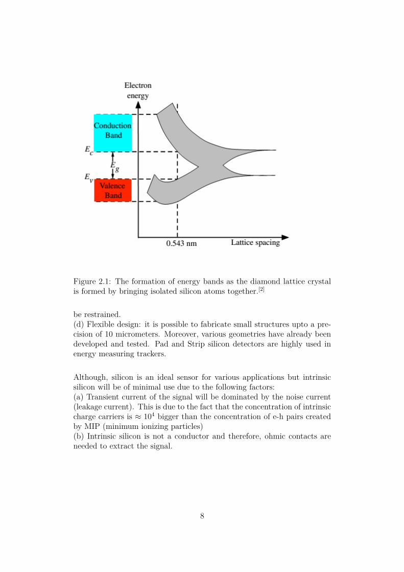
Figure 2.1: The formation of energy bands as the diamond lattice crystalis formed by bringing isolated silicon atoms together.[2]
be restrained.(d) Flexible design: it is possible to fabricate small structures upto a pre-cision of 10 micrometers. Moreover, various geometries have already beendeveloped and tested. Pad and Strip silicon detectors are highly used inenergy measuring trackers.
Although, silicon is an ideal sensor for various applications but intrinsicsilicon will be of minimal use due to the following factors:(a) Transient current of the signal will be dominated by the noise current(leakage current). This is due to the fact that the concentration of intrinsiccharge carriers is ≈ 104 bigger than the concentration of e-h pairs createdby MIP (minimum ionizing particles)(b) Intrinsic silicon is not a conductor and therefore, ohmic contacts areneeded to extract the signal.
8
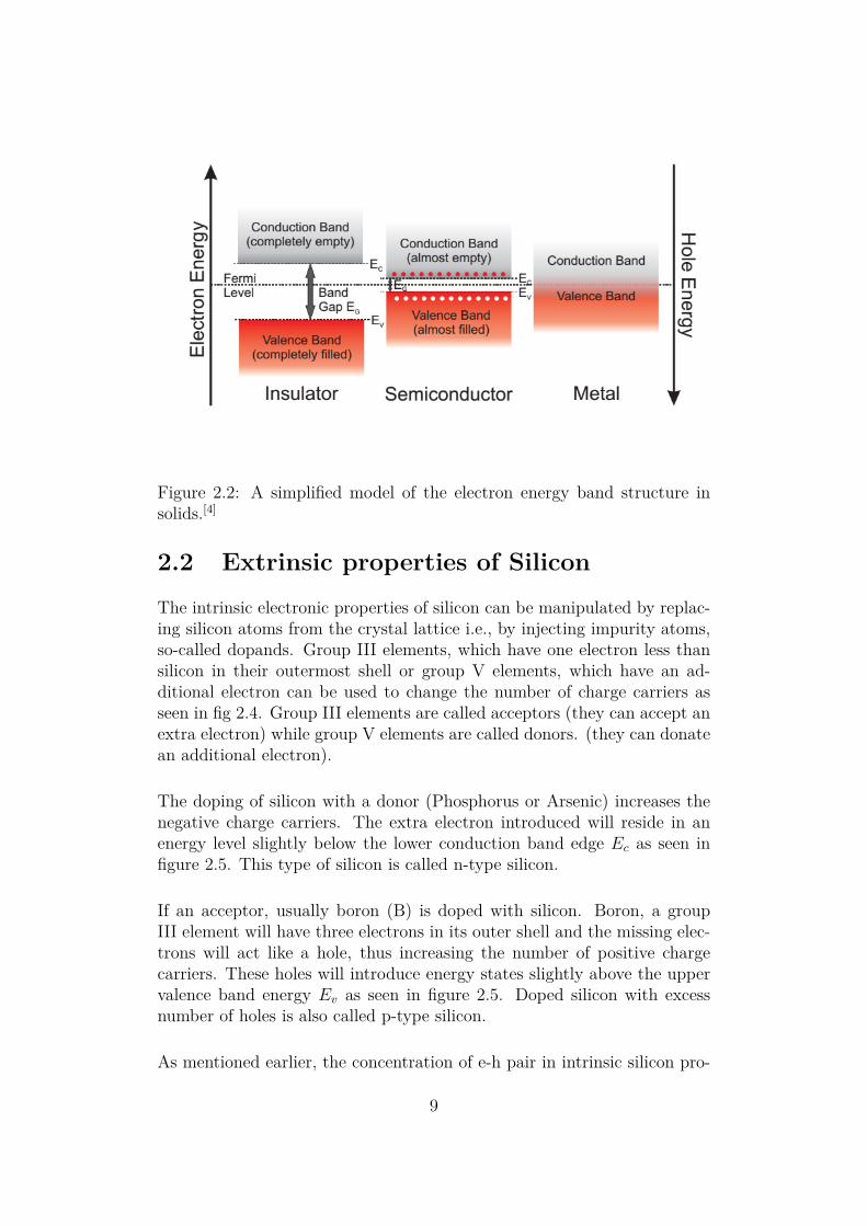
Figure 2.2: A simplified model of the electron energy band structure insolids.[4]
2.2 Extrinsic properties of Silicon
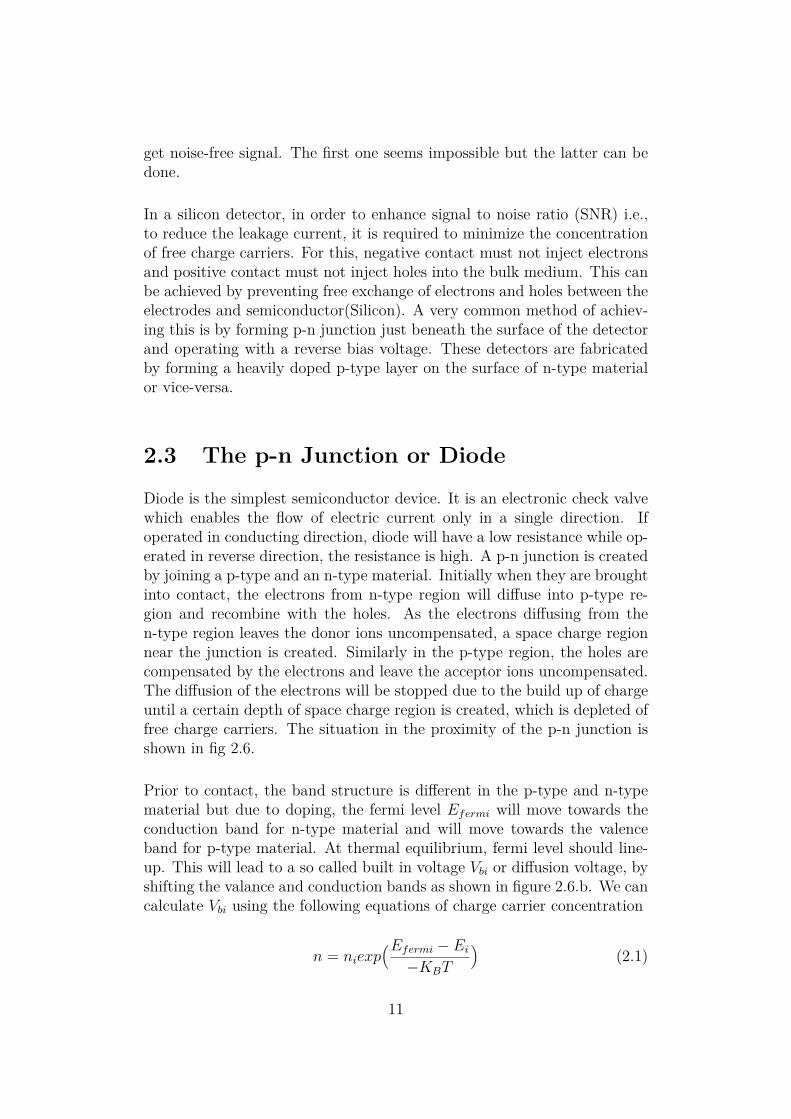
The intrinsic electronic properties of silicon can be manipulated by replac-ing silicon atoms from the crystal lattice i.e., by injecting impurity atoms,so-called dopands. Group III elements, which have one electron less thansilicon in their outermost shell or group V elements, which have an ad-ditional electron can be used to change the number of charge carriers asseen in fig 2.4. Group III elements are called acceptors (they can accept anextra electron) while group V elements are called donors. (they can donatean additional electron).
The doping of silicon with a donor (Phosphorus or Arsenic) increases thenegative charge carriers. The extra electron introduced will reside in anenergy level slightly below the lower conduction band edge Ec as seen infigure 2.5. This type of silicon is called n-type silicon.
If an acceptor, usually boron (B) is doped with silicon. Boron, a groupIII element will have three electrons in its outer shell and the missing elec-trons will act like a hole, thus increasing the number of positive chargecarriers. These holes will introduce energy states slightly above the uppervalence band energy Ev as seen in figure 2.5. Doped silicon with excessnumber of holes is also called p-type silicon.
As mentioned earlier, the concentration of e-h pair in intrinsic silicon pro-
9
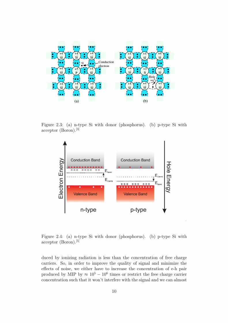
Figure 2.3: (a) n-type Si with donor (phosphorus). (b) p-type Si withacceptor (Boron).[3]
Figure 2.4: (a) n-type Si with donor (phosphorus). (b) p-type Si withacceptor (Boron).[5]
duced by ionizing radiation is less than the concentration of free chargecarriers. So, in order to improve the quality of signal and minimize theeffects of noise, we either have to increase the concentration of e-h pairproduced by MIP by ≈ 105 − 106 times or restrict the free charge carrierconcentration such that it won’t interfere with the signal and we can almost
10
get noise-free signal. The first one seems impossible but the latter can bedone.
In a silicon detector, in order to enhance signal to noise ratio (SNR) i.e.,to reduce the leakage current, it is required to minimize the concentrationof free charge carriers. For this, negative contact must not inject electronsand positive contact must not inject holes into the bulk medium. This canbe achieved by preventing free exchange of electrons and holes between theelectrodes and semiconductor(Silicon). A very common method of achiev-ing this is by forming p-n junction just beneath the surface of the detectorand operating with a reverse bias voltage. These detectors are fabricatedby forming a heavily doped p-type layer on the surface of n-type materialor vice-versa.
2.3 The p-n Junction or Diode
Diode is the simplest semiconductor device. It is an electronic check valvewhich enables the flow of electric current only in a single direction. Ifoperated in conducting direction, diode will have a low resistance while op-erated in reverse direction, the resistance is high. A p-n junction is createdby joining a p-type and an n-type material. Initially when they are broughtinto contact, the electrons from n-type region will diffuse into p-type re-gion and recombine with the holes. As the electrons diffusing from then-type region leaves the donor ions uncompensated, a space charge regionnear the junction is created. Similarly in the p-type region, the holes arecompensated by the electrons and leave the acceptor ions uncompensated.The diffusion of the electrons will be stopped due to the build up of chargeuntil a certain depth of space charge region is created, which is depleted offree charge carriers. The situation in the proximity of the p-n junction isshown in fig 2.6.
Prior to contact, the band structure is different in the p-type and n-typematerial but due to doping, the fermi level Efermi will move towards theconduction band for n-type material and will move towards the valenceband for p-type material. At thermal equilibrium, fermi level should line-up. This will lead to a so called built in voltage Vbi or diffusion voltage, byshifting the valance and conduction bands as shown in figure 2.6.b. We cancalculate Vbi using the following equations of charge carrier concentration
n = niexp(Efermi − Ei
−KBT
)(2.1)
11
p = niexp(Ei − Efermi
−KBT
)(2.2)
and setting the majority carrier concentrations equal to the donor andacceptor concentrations:
nn = ND pp = NA (2.3)
ND ·NA = ni2exp
(Epi − En
i
KT
)(2.4)
Vbi = 1q
(Epi − En
i ) = KT
qln(NDNA
n2i
)(2.5)
The size of the depleted zones in the n-type (dp) and p-type (dn) materialcan be calculated using the following expressions:
dp =√
2εεqe
ND
ND(NA +ND)Vbi (2.6)
dn =√
2εεqe
NA
ND(NA +ND)Vbi (2.7)
d = dn + dp =√
2εε(NA +ND)qeNDNA
Vbi (2.8)
Generally, p-n junctions are usually formed using a low doped material forpractical applications, where a certain region gets highly doped towardsthe opposite type. The p-n junction is formed at the edge of the highlydoped region which is in contact to the surrounding bulk with low dopingconcentration of opposite dopands. In this realistic case where the dopingconcentration on one side of the junction is significantly higher than on theopposite side (e.g. NA >>ND), equation 2.8 becomes:
d =√
2εεqeND
Vbi (2.9)
If an external voltage is applied across the p-n junction, the system willnot be in the thermal equilibrium anymore. The charge carriers will startto drift according to the electric field and depending on the polarity of theapplied voltage, the width of the space charge region will shrink (forward
12
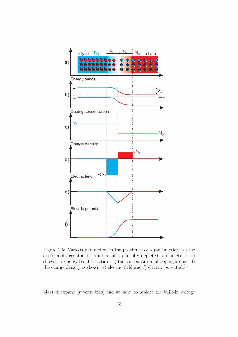
Figure 2.5: Various parameters in the proximity of a p-n junction. a) thedonor and acceptor distribution of a partially depleted p-n junction. b)shows the energy band structure. c) the concentration of doping atoms. d)the charge density is shown, e) electric field and f) electric potential.[5]
bias) or expand (reverse bias) and we have to replace the built-in voltage
13
Vbi with Vbi - V :
d =√
2εε(NA +ND)qeNDNA
(Vbi − V ) (2.10)
For the realistic case as discussed above with NA >>ND, equation 2.10simplifies to
d =√
2εεqeND
(Vbi − V ) (2.11)
14
Chapter 3
Silicon Strip Detector
In this chapter, we will discuss about the working principle of silicon de-tector and the design process of a silicon strip detector.
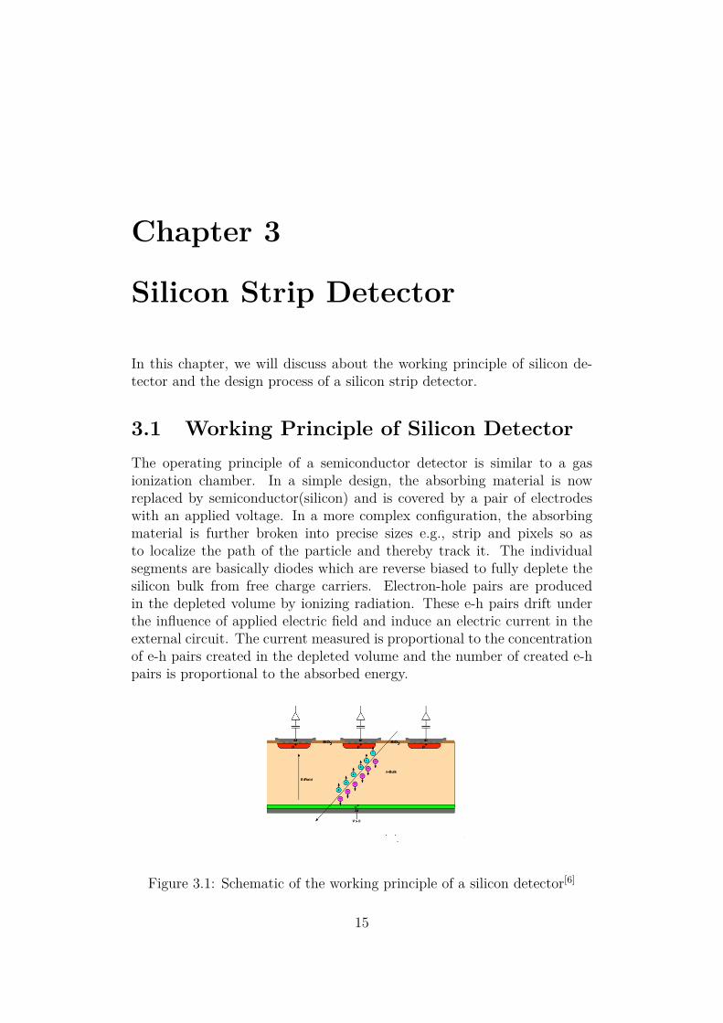
3.1 Working Principle of Silicon DetectorThe operating principle of a semiconductor detector is similar to a gasionization chamber. In a simple design, the absorbing material is nowreplaced by semiconductor(silicon) and is covered by a pair of electrodeswith an applied voltage. In a more complex configuration, the absorbingmaterial is further broken into precise sizes e.g., strip and pixels so asto localize the path of the particle and thereby track it. The individualsegments are basically diodes which are reverse biased to fully deplete thesilicon bulk from free charge carriers. Electron-hole pairs are producedin the depleted volume by ionizing radiation. These e-h pairs drift underthe influence of applied electric field and induce an electric current in theexternal circuit. The current measured is proportional to the concentrationof e-h pairs created in the depleted volume and the number of created e-hpairs is proportional to the absorbed energy.
Figure 3.1: Schematic of the working principle of a silicon detector[6]
15
3.2 Design Basics of Silicon Strip DetectorIt is possible to detect a particle hitting the detector using the basic princi-ple described in the previous section. But, it won’t give us any additionalinformation regarding the site of hit on the detector. By creating smallersensing elements which are electrically isolated from each other using thesame principle, we can achieve this. Strip detector is one such geometryused in detecting the particles.
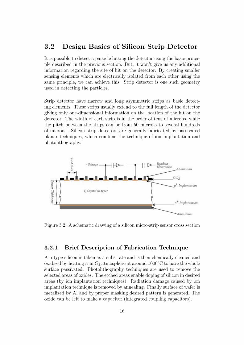
Strip detector have narrow and long asymmetric strips as basic detect-ing elements. These strips usually extend to the full length of the detectorgiving only one-dimensional information on the location of the hit on thedetector. The width of each strip is in the order of tens of microns, whilethe pitch between the strips can be from 50 microns to several hundredsof microns. Silicon strip detectors are generally fabricated by passivatedplanar techniques, which combine the technique of ion implantation andphotolithography.
Figure 3.2: A schematic drawing of a silicon micro-strip sensor cross section
3.2.1 Brief Description of Fabrication TechniqueA n-type silicon is taken as a substrate and is then chemically cleaned andoxidised by heating it in O2 atmosphere at around 1000oC to have the wholesurface passivated. Photolithography techniques are used to remove theselected areas of oxides. The etched areas enable doping of silicon in desiredareas (by ion implantation techniques). Radiation damage caused by ionimplantation technique is removed by annealing. Finally surface of wafer ismetalized by Al and by proper masking desired pattern is generated. Theoxide can be left to make a capacitor (integrated coupling capacitors).
16
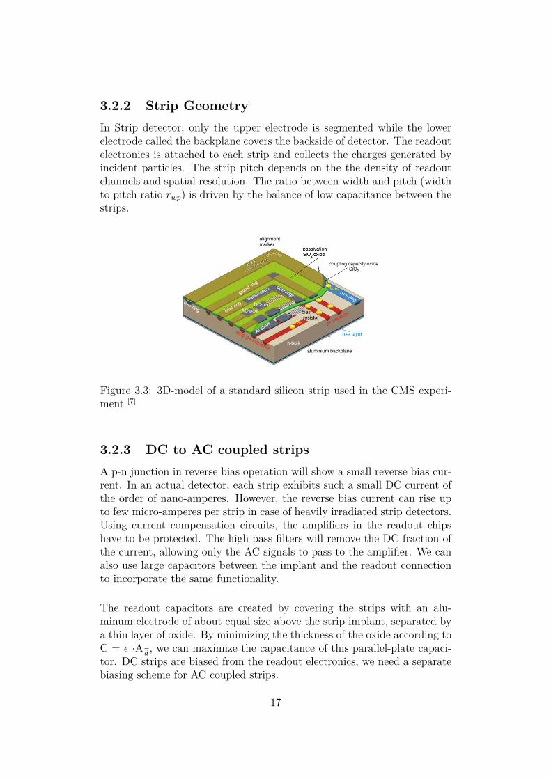
3.2.2 Strip GeometryIn Strip detector, only the upper electrode is segmented while the lowerelectrode called the backplane covers the backside of detector. The readoutelectronics is attached to each strip and collects the charges generated byincident particles. The strip pitch depends on the the density of readoutchannels and spatial resolution. The ratio between width and pitch (widthto pitch ratio rwp) is driven by the balance of low capacitance between thestrips.
Figure 3.3: 3D-model of a standard silicon strip used in the CMS experi-ment [7]
3.2.3 DC to AC coupled stripsA p-n junction in reverse bias operation will show a small reverse bias cur-rent. In an actual detector, each strip exhibits such a small DC current ofthe order of nano-amperes. However, the reverse bias current can rise upto few micro-amperes per strip in case of heavily irradiated strip detectors.Using current compensation circuits, the amplifiers in the readout chipshave to be protected. The high pass filters will remove the DC fraction ofthe current, allowing only the AC signals to pass to the amplifier. We canalso use large capacitors between the implant and the readout connectionto incorporate the same functionality.
The readout capacitors are created by covering the strips with an alu-minum electrode of about equal size above the strip implant, separated bya thin layer of oxide. By minimizing the thickness of the oxide according toC = ε ·A
d, we can maximize the capacitance of this parallel-plate capaci-
tor. DC strips are biased from the readout electronics, we need a separatebiasing scheme for AC coupled strips.
17
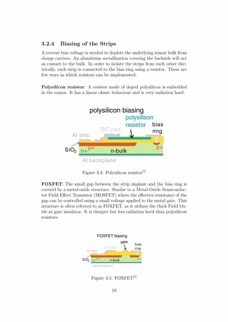
3.2.4 Biasing of the StripsA reverse bias voltage is needed to deplete the underlying sensor bulk fromcharge carriers. An aluminium metallisation covering the backside will actas contact to the bulk. In order to isolate the strips from each other elec-trically, each strip is connected to the bias ring using a resistor. These arefew ways in which resistors can be implemented:
Polysilicon resistor: A resistor made of doped polysilicon is embeddedin the sensor. It has a linear ohmic behaviour and is very radiation hard.
Figure 3.4: Polysilicon resistor[7]
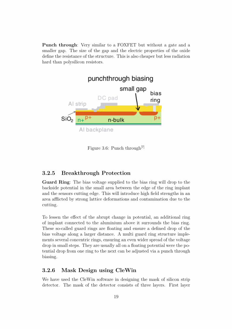
FOXFET: The small gap between the strip implant and the bias ring iscovered by a metal-oxide structure. Similar to a Metal-Oxide Semiconduc-tor Field Effect Transistor (MOSFET) where the effective resistance of thegap can be controlled using a small voltage applied to the metal gate. Thisstructure is often referred to as FOXFET, as it utilizes the thick Field Ox-ide as gate insulator. It is cheaper but less radiation hard than polysiliconresistors.
Figure 3.5: FOXFET[7]
18
Punch through: Very similar to a FOXFET but without a gate and asmaller gap. The size of the gap and the electric properties of the oxidedefine the resistance of the structure. This is also cheaper but less radiationhard than polysilicon resistors.
Figure 3.6: Punch through[7]
3.2.5 Breakthrough ProtectionGuard Ring: The bias voltage supplied to the bias ring will drop to thebackside potential in the small area between the edge of the ring implantand the sensors cutting edge. This will introduce high field strengths in anarea afflicted by strong lattice deformations and contamination due to thecutting.
To lessen the effect of the abrupt change in potential, an additional ringof implant connected to the aluminium above it surrounds the bias ring.These so-called guard rings are floating and ensure a defined drop of thebias voltage along a larger distance. A multi guard ring structure imple-ments several concentric rings, ensuring an even wider spread of the voltagedrop in small steps. They are usually all on a floating potential were the po-tential drop from one ring to the next can be adjusted via a punch throughbiasing.
3.2.6 Mask Design using CleWinWe have used the CleWin software in designing the mask of silicon stripdetector. The mask of the detector consists of three layers. First layer
19
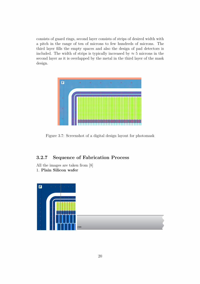
consists of guard rings, second layer consists of strips of desired width witha pitch in the range of ten of microns to few hundreds of microns. Thethird layer fills the empty spaces and also the design of pad detectors isincluded. The width of strips is typically increased by ≈ 5 microns in thesecond layer as it is overlapped by the metal in the third layer of the maskdesign.
Figure 3.7: Screenshot of a digital design layout for photomask
3.2.7 Sequence of Fabrication ProcessAll the images are taken from [8]1. Plain Silicon wafer
20
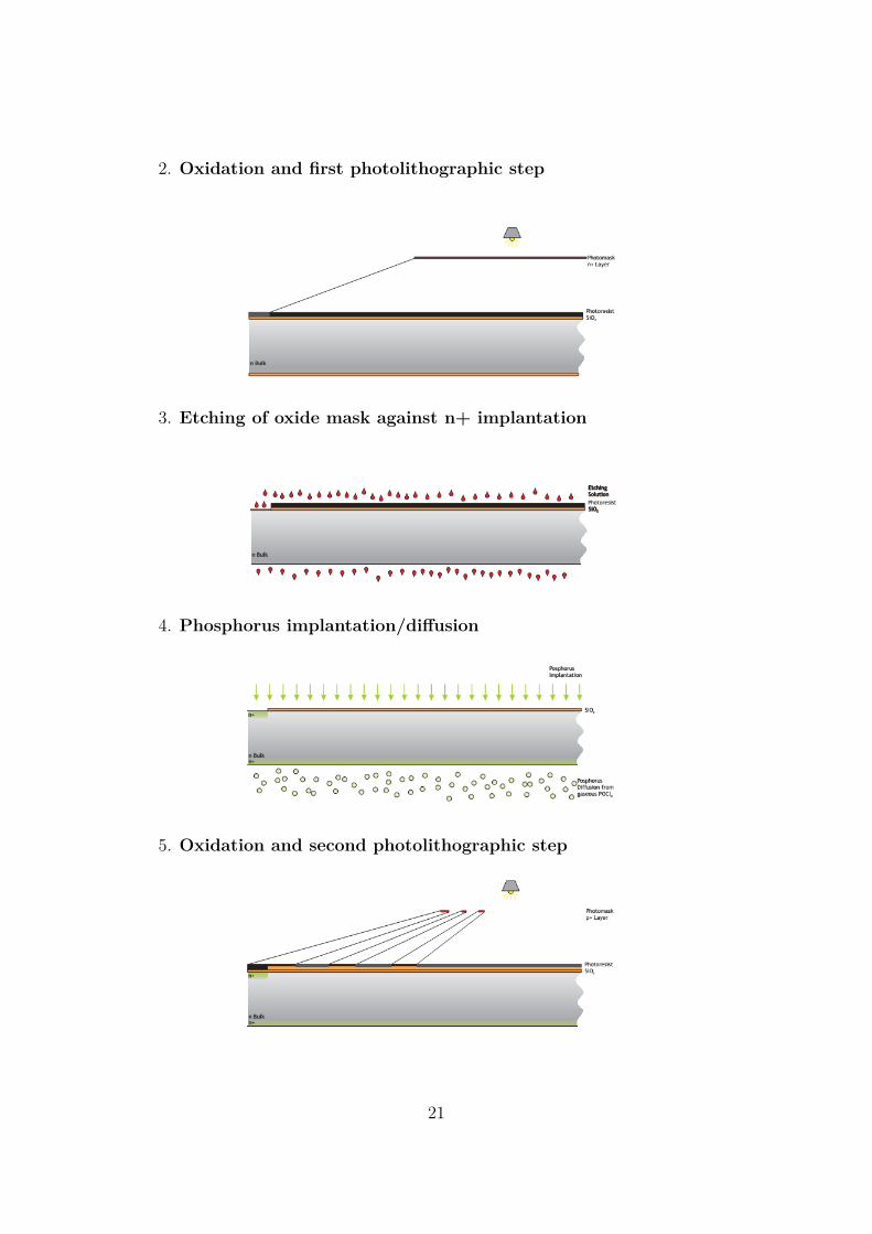
2. Oxidation and first photolithographic step
3. Etching of oxide mask against n+ implantation
4. Phosphorus implantation/diffusion
5. Oxidation and second photolithographic step
21
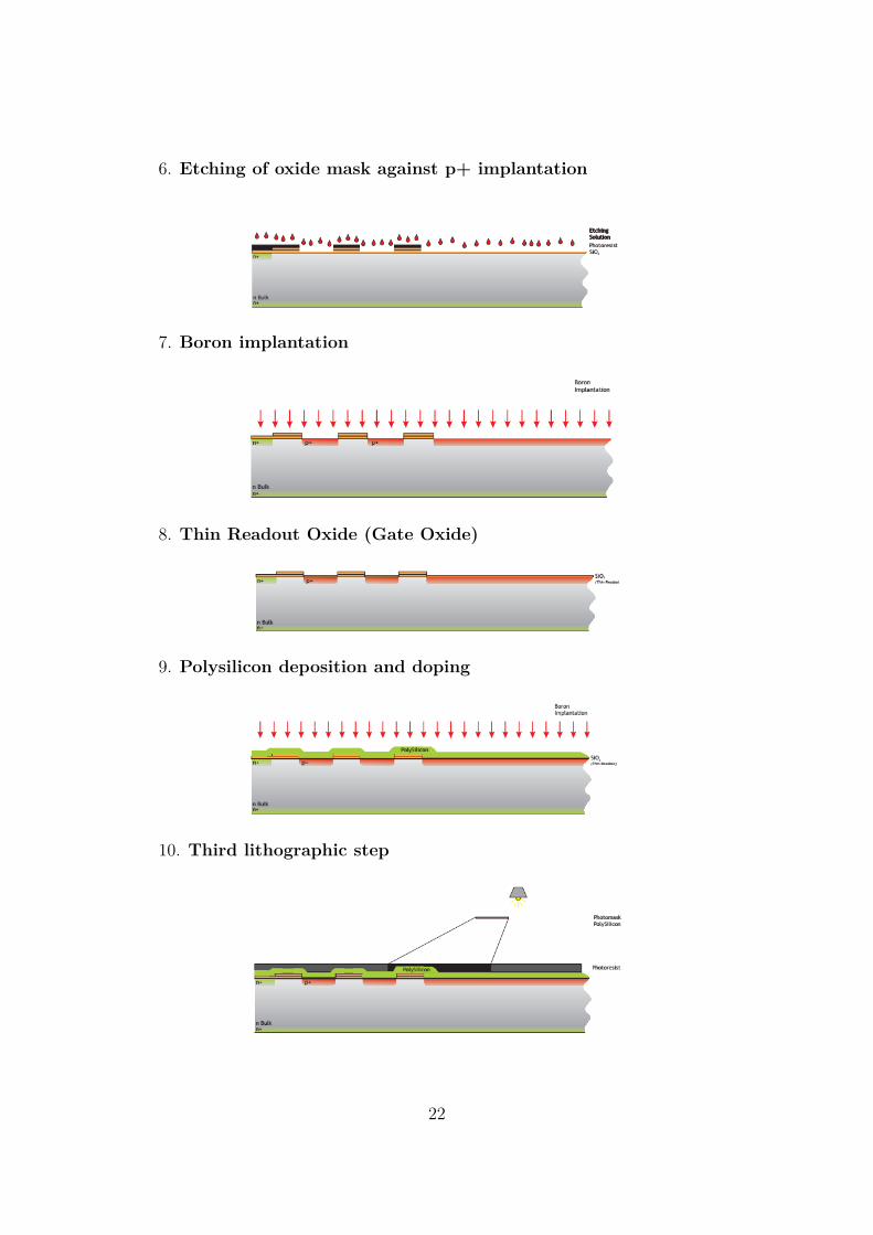
6. Etching of oxide mask against p+ implantation
7. Boron implantation
8. Thin Readout Oxide (Gate Oxide)
9. Polysilicon deposition and doping
10. Third lithographic step
22
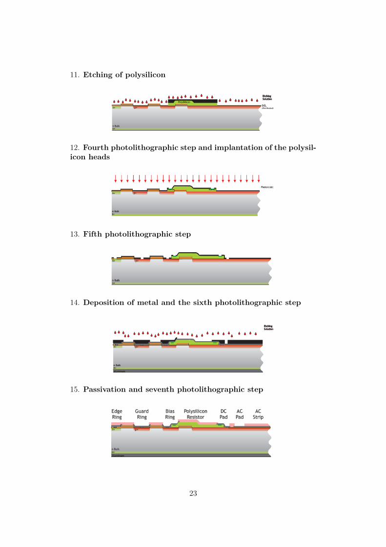
11. Etching of polysilicon
12. Fourth photolithographic step and implantation of the polysil-icon heads
13. Fifth photolithographic step
14. Deposition of metal and the sixth photolithographic step
15. Passivation and seventh photolithographic step
23

3.2.8 SummaryA detailed study about material properties of silicon and semiconductordevice physics of silicon has been done. I studied about the working prin-ciple of silicon detectors and design of silicon strip detectors. I have learntCleWin software used in the designing of detector mask.
24
References
[1] Nuclear Radiation Detectors, S.S. Kapoor, V. S. Ramamurthy. WileyEastern Limited.[2] S. M. Sze, M.-K. Lee, Semiconductor Devices: Physics and Technology,John Wiley Sons, 2012.[3] Energy for Electron-Hole Pair Generation in Silicon by Electrons and αParticles[4] Adapted from Prof. Dr. Hans-Christian Schultz-Coulon Lecture Notes[5] G. Lutz. Semiconductor Radiation Detectors: Device Physics. Springer,Berlin, 2007.[6] Adapted from lecture notes of Prof. Helmuth Spieler[7] F. Hartmann. Evolution of Silicon Sensor Technology in Particle Physics,volume 231 of Springer Tracts in Modern Physics. Springer, 2009.[8] The New Silicon Strip Detectors for the CMS Tracker Upgrade[9] Design of a Radiation Hard Silicon Pixel Sensor for X-ray Science.[10] Characterization of Single Sided Silicon Microstrip Detector
25