
Silicon Mie Resonators for Highly Directional Light...
31
1 Silicon Mie Resonators for Highly Directional Light Emission from monolayer MoS 2 Ahmet Fatih Cihan 1 , Alberto G. Curto 1,2 , Søren Raza 1 , Pieter G. Kik 1,3 and Mark L. Brongersma 1 1. Geballe Laboratory for Advanced Materials, Stanford University, Stanford, California 94305, United States 2. Dep. Applied Physics and Institute for Photonic Integration, Eindhoven University of Technology, 5600 MB Eindhoven, The Netherlands 3. CREOL, The College of Optics and Photonics, University of Central Florida, Florida 32816, United States Abstract: Controlling light emission from quantum emitters has important applications ranging from solid-state lighting and displays to nanoscale single-photon sources. Optical antennas have emerged as promising tools to achieve such control right at the location of the emitter, without the need for bulky, external optics. Semiconductor nanoantennas are particularly practical for this purpose because simple geometries, such as wires and spheres, support multiple, degenerate optical resonances. Here, we start by modifying Mie scattering theory developed for plane wave illumination to describe scattering of dipole emission. We then use this theory and experiments to demonstrate several pathways to achieve control over the directionality, polarization state, and spectral emission that rely on a coherent coupling of an emitting dipole to optical resonances of a Si nanowire. A forward-to-backward ratio of 20 was demonstrated for the electric dipole emission at 680 nm from a monolayer MoS 2 by optically coupling it to a Si nanowire.
Transcript of Silicon Mie Resonators for Highly Directional Light...

1
Silicon Mie Resonators for Highly Directional Light Emission from
monolayer MoS2
Ahmet Fatih Cihan1, Alberto G. Curto1,2, Søren Raza1, Pieter G. Kik1,3
and Mark L. Brongersma1
1. Geballe Laboratory for Advanced Materials, Stanford University, Stanford, California 94305, United States
2. Dep. Applied Physics and Institute for Photonic Integration, Eindhoven University of Technology, 5600 MB Eindhoven, The Netherlands
3. CREOL, The College of Optics and Photonics, University of Central Florida, Florida 32816, United States
Abstract:
Controlling light emission from quantum emitters has important applications ranging from
solid-state lighting and displays to nanoscale single-photon sources. Optical antennas have
emerged as promising tools to achieve such control right at the location of the emitter, without
the need for bulky, external optics. Semiconductor nanoantennas are particularly practical for
this purpose because simple geometries, such as wires and spheres, support multiple,
degenerate optical resonances. Here, we start by modifying Mie scattering theory developed
for plane wave illumination to describe scattering of dipole emission. We then use this theory
and experiments to demonstrate several pathways to achieve control over the directionality,
polarization state, and spectral emission that rely on a coherent coupling of an emitting dipole
to optical resonances of a Si nanowire. A forward-to-backward ratio of 20 was demonstrated
for the electric dipole emission at 680 nm from a monolayer MoS2 by optically coupling it to a
Si nanowire.

2
Main text:
Achieving control over the radiation properties of quantum emitters is key to improving
efficiency and realizing new functionality in optoelectronic systems. Bulky optical components
have been developed for many years and are extremely effective in controlling the angular,
polarization, and spectral properties of light emission. Recent advances in the fields of metallic
and dielectric optical metamaterials and nanoantennas have now also enabled effective
integration of solid-state emitters and control elements into inexpensive platforms.1–3 Such
structures can manipulate light emission in the near-field of an emitter and thus hold a real
promise to achieve even greater control over the emission process. For example, we will show
how the undesired losses due to radiation of quantum emitters into a high-index substrate can
be reduced by redirecting the emission upward with an antenna.
Whereas structures based on noble metals are currently most advanced in manipulating
light-matter interaction at the nanoscale, they typically are complex in shape, display undesired
optical losses, and are not compatible with most semiconductor device processing
technologies. High-index semiconductor antennas can circumvent these issues while providing
complex electrical and optical functions.2,4–14 Based on the mature fabrication infrastructure,
silicon nanostructures appear particularly promising for optoelectronic applications.4,9–12,15–17
Semiconductor nanoparticles of simple geometric shapes have displayed directional scattering
of plane waves when the renowned Kerker conditions are satisfied.12,16,18 When these conditions
are met, directionality is naturally achieved through the coherent excitation of electric and
magnetic dipole resonances in the particle and tuning the interference of the associated
scattered fields.12,19,20 Thanks to their high refractive indices, semiconductor nanoparticles can
satisfy the Kerker conditions in the visible spectral range.16,18,21 Given the ever-increasing
importance of solid state light emitters and quantum nanophotonics, it is of great interest to

3
explore whether analogous conditions can be identified that will facilitate directional emission
from quantum emitters and we answer this is important question positively in this work. As
such, it nicely complements other low-loss approaches involving advanced semiconductor
photonic crystals and leaky wave antenna structures to control spectral and angular emission
properties.22–27
Directional emission with the help of nanometallic antennas has been analyzed
theoretically in great detail and was demonstrated experimentally at optical frequencies.28–33
For semiconductor antennas, however, directional emission exploiting Mie resonances has
been limited to theoretical proposals16,34–46 or experiments in the microwave regime.47 By
modifying the conventional Mie theory to describe light scattering by a nanowire (NW) from
a dipolar source as opposed to the standard plane-wave source, we reveal that directional
emission with a silicon NW can be realized through a variety of mechanisms. Each of these
directionality mechanisms involves optical interference effects that come about when the light
emitted from a quantum emitter can follow different pathways to the far-field. For example,
highly-directional emission can occur when a fraction of the light emitted by an electric dipole
source is rescattered by exciting the dominant electric dipole resonance of a nearby NW. It can
also follow from the coherent excitation of electric and magnetic dipoles in a NW, more akin
to the original directional Kerker scattering.38 Experimental evidence is provided for both of
these directionality mechanisms by coupling the exciton emission from an atomically thin layer
of MoS2 48–52 to two differently-sized Si NWs. We demonstrate a forward-to-backward emission
ratio of 20 from MoS2 emitters coupled to Si NWs at visible wavelengths. The use of a 2D
semiconductor enables the realization of an accurate and repeatable separation between the
emitter and NW, which is critical for obtaining reliable control over the direction of light
emission.37 Furthermore, 2D materials such as MoS2 benefit from the simplicity and low-cost
nature of available deposition/growth techniques making them particularly promising for

4
future photonic device applications compared to conventional epitaxially-grown emitter
materials.53–56
Conventional Mie theory allows us to calculate the excited resonances for an infinitely
long cylinder under plane-wave illumination (See Fig. 1a for the excitation geometry) by
expanding the incident and scattered fields in terms of cylindrical harmonics.57 The expansion
coefficients in the scattered field are referred to as Mie coefficients and they quantify the
scattering contributions from different resonances, e.g. electric and magnetic dipoles (see
Figure 1b for a multipolar decomposition of the scattering efficiency Qscat for an infinitely long
Si NW). When Mie coefficients corresponding to the electric and magnetic dipoles excited by
a plane wave have equal amplitude and phase, the scattered fields originating from these
resonances destructively interfere in the backward direction, satisfying the so-called 1st Kerker
condition.19 This condition has played a central role in the research on light-matter interactions
with high-index nanostructures.3 In this work we will go beyond plane wave excitation and
explore the impact of using the electric dipole emission from the MoS2 monolayer as our
source. We show that the choice of a localized source can profoundly influence the weights of
the excited NW resonances compared to the plane-wave case. This naturally results in different
conditions for emission directionality. To gain an intuitive understanding of the origin of these
modifications, we derive an analytic expression for the scattering efficiency of a cylindrical
NW for electric dipole radiation in two dimensions (2D):
𝑄"#$%&'()*+ = -./01
-23/= 𝑏5 6 𝐻5
8 𝑘: 𝑅 + 𝑑6.?
5@A? (1)
Here, 𝑃"#$% and 𝑃'D# are the scattered and incident source-dipole radiation powers respectively,
bn are the conventional Mie coefficients found from the plane-wave excitation problem,57 Hn(1)
are Hankel functions of the first kind, 𝑘: = 2𝜋/𝜆 is the free-space wave vector, 𝑅 is the NW
radius and 𝑑 is the dipole-NW distance (see Supplementary Information for the derivation of
Eq. 1). Note that in this 2D analysis, the excitation source is a line dipole and the NW is

5
infinitely long.57,58 Whereas a 3D theory would be needed to quantitatively predict the correct
magnitude for the scattering efficiency for a point dipole source, we show that this simple 2D
description can explain the role of the different multipolar excitations in achieving directional
emission and the importance of controlling the NW-emitter distance.37 This is particularly true
as, for symmetry reasons, the far-field radiation patterns seen for an infinitesimal electric point-
dipole (3D) and an electric line-source (2D) are identical in the plane orthogonal to the NW-
axis and intersecting the emitter. (See Supplementary Fig. S2). Hence, the scattered far-field
radiation pattern in this plane will also be identical in both cases.45
As can be seen in Eq. 1, each term in the expression for the scattering efficiency can be
associated with a specific resonance. Each of the resonant contributions has a distance
dependent weighting factor that is given by the Hankel function relevant to that resonance. The
origin of this Hankel function dependence arises as the scattered power related to the
interaction of the dipole source and NW scattered fields, which are both described by Hankel
functions. Because of these weighting factors, the excitation efficiencies for different
multipoles display different dependences on the dipole-NW distance, which makes this
distance an important parameter determining the directionality of the overall emission. The
scattering behavior of the NW under dipole illumination approaches that seen for plane wave
illumination when the dipole source is far away (𝑑 ≫ 𝜆) from the NW (Supplementary Figure
S1). However, when the dipole is brought closer to the NW as in Fig. 1c, the excitation of
different resonances takes place with different strengths resulting in a modified scattering
spectrum (Fig. 1d).
The dipole emission directionality (Fig. 1c) is different from the plane wave scattering
directionality not only because of the modified resonance contributions but also because of the
non-directional nature of the source.38 In other words, to achieve the desired emission
directionality, it is important to consider the interference of the incident fields from the source
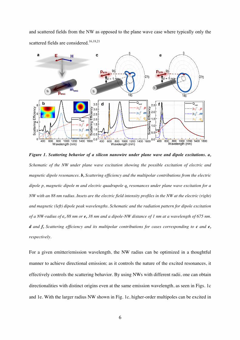
6
and scattered fields from the NW as opposed to the plane wave case where typically only the
scattered fields are considered.16,18,21
Figure 1. Scattering behavior of a silicon nanowire under plane wave and dipole excitations. a,
Schematic of the NW under plane wave excitation showing the possible excitation of electric and
magnetic dipole resonances. b, Scattering efficiency and the multipolar contributions from the electric
dipole p, magnetic dipole m and electric quadrupole qe resonances under plane wave excitation for a
NW with an 88 nm radius. Insets are the electric field intensity profiles in the NW at the electric (right)
and magnetic (left) dipole peak wavelengths. Schematic and the radiation pattern for dipole excitation
of a NW-radius of c, 88 nm or e, 38 nm and a dipole-NW distance of 1 nm at a wavelength of 675 nm.
d and f, Scattering efficiency and its multipolar contributions for cases corresponding to c and e,
respectively.
For a given emitter/emission wavelength, the NW radius can be optimized in a thoughtful
manner to achieve directional emission; as it controls the nature of the excited resonances, it
effectively controls the scattering behavior. By using NWs with different radii, one can obtain
directionalities with distinct origins even at the same emission wavelength, as seen in Figs. 1c
and 1e. With the larger radius NW shown in Fig. 1c, higher-order multipoles can be excited in
7
the emission band of MoS2 in the range from 650-720 nm, resulting in directionality due to the
interference of the scattered fields originating from these multipoles and the emitter dipole. On
the other hand, with the smaller NW of Fig. 1e, we can observe directional emission due to the
interference of the scattered fields from the excited electric dipole NW resonance with those
of the emitter dipole.
To experimentally investigate the emission directionality, we use a confocal optical
microscope with a laser excitation wavelength of 633 nm that affords both top and bottom
detection of photoluminescence (PL) signals (see Methods). As the emitter, we use monolayer
MoS2 grown on a transparent sapphire substrate. Si NWs are drop-cast on top, as shown in Fig.
2a. In one experiment, we use a tapered Si NW whose radius gradually varies from around 20
nm to 40 nm over a length of 40 µm. The gently tapered shape of the NW makes it convenient
to match the spectrum of the emitter to the different diameter-dependent NW resonances that
give rise to directionality.
Images of the transverse magnetic (TM) polarized emission are taken from the top and
bottom of the sample (Fig. 2b,c). They show that the NW enhances the emission of the MoS2
layer to the top (i.e forward-direction) while suppressing the emission to the bottom (i.e.
backward direction). The top-to-bottom (T/B) ratio for the emission, provided in Fig. 2d,
reaches values up to 2.5 on the NW while that of bare MoS2 areas is about 0.8 (see Methods
for the procedure to correct for the contribution of the detection system to the measured
asymmetry). An important caveat of the measurement in Fig. 2d is that the detection system is
diffraction-limited, and consequently the region from which photoluminescence is collected is
significantly larger than the NW diameter. This results in a reduced T/B ratio compared to our
simulations due to the contributions from the bare MoS2 regions adjacent to the NW which
produce non-directional emission. In order to eliminate this unwanted effect and measure the

8
ultimate directionality observable for emitters under the antenna, the sample is etched using a
low-energy Ar plasma where the NW itself acts as an etching mask (see Fig. 2e).
Figure 2. Experimental demonstration of highly directional emission in fluorescence images. a,
Schematic and dark-field scattering image of an un-etched MoS2 sample. The scale bar corresponds to
5 µm. b, c, Top (T) and bottom (B) fluorescence images of the sample for TM polarization. d, T/B ratio
normalized such that the bare MoS2 T/B ratio is ca. 0.8, as predicted by optical simulations for this
elementary system (see Methods). e-h, Corresponding images for the sample after etching the MoS2
around the NW. Inset to panel h shows that the T/B ratio for the TE polarization displays no noticeable
enhancement. The arrows indicate the electric field polarization direction for the collected light.

9
The top and bottom fluorescence images after the etching process show that the emission is
almost entirely eliminated from the bare MoS2 regions, except for isolated spots corresponding
to areas of few-layer MoS2, while the emission from the emitters under the NW is maintained
(Fig. 2f, g). Note that the bottom emission around the lower half of the NW in Figure 2g is
almost completely suppressed, suggestive of a very high directionality (see Supplementary
Information for top and bottom line scans of the emission across the NW). As can be seen in
Figure 2h, the T/B ratio is more than 20 on the part of the tapered NW whereas that of the
reference bare MoS2 is around 0.8. Therefore, it can be concluded that the NW directionality
enhancement over bare MoS2 is more than 25-fold.
As a control experiment, we provide the T/B ratio of the same NW for TE polarized
collection in the inset of Figure 2h. Here, the NW is barely discernable in the T/B ratio image
implying that the enhanced directionality seen for the TM case is linked to multipolar
resonances capable of redirecting the emission with this polarization state.
In order to explore the nature of the observed directional emission, we use our analytical
Mie theory to calculate the T/B emission ratio. Within this approach, the far-field emission
intensity is given as:
IKK 𝜃 = MNOPNQN
RS−𝑖 5 𝐽5 𝑘:(𝑅 + 𝑑) − 𝑏5𝐻5
8 𝑘:(𝑅 + 𝑑) 𝑒AZ5[?5@A?
6 (2)
where 𝐽5 is the Bessel function of the first kind, I is the current of the line source, and q is the
emission angle (see Supplementary Information for the derivation). By integrating the far-field
intensity values in Eq. (2) around the forward (q = p) and backward (q = 0) directions, we
obtain the spectral and NW size dependence of the T/B emission ratio (see Methods). Figure
3a shows a map of these calculations, revealing multiple clear bands with high T/B ratios. Each
band can be identified with a unique directionality mechanism involving different multipolar
resonances. Very similar results are obtained with FDTD simulations that include the presence
of the substrate, as shown in supplementary Fig. S4.

10
For the emission wavelength range of MoS2 (the vertical shaded area in Fig. 3a), it is
possible to capture two directionality mechanisms with NWs that feature radii below 100 nm.
In order to identify how the different multipoles contribute to each mechanism, we determine
the far-field complex electric field contributions in the backward direction from several
multipolar resonances. We first analyze the smaller, tapered NW for which the high
directionality was verified in Fig. 2. Its radius range from 20 nm – 40 nm is indicated by the
lower grey-shaded band. For a selected 38 nm radius NW, these relevant field contributions
are shown in the left panel of Fig. 3b in a phasor representation to clearly show their relative
magnitudes and phases. It is clear that for this wire the excitation of an electric dipole (pexc)
resonance alone suffices to almost fully cancel out the incident field originating from the source
dipole in the backward direction. There is only a very small contribution related to the magnetic
dipole mexc. However, for a larger 88 nm-radius NW (right panel of Fig. 3b), fields from the
electric dipole, magnetic dipole and electric quadrupole resonances (pexc, mexc and qexc,
respectively), are more-or-less equal in magnitude. This corresponds results in very little
backward emission and in this case we find that the directionality can primarily be attributed
to the coherent excitation of electric and magnetic dipole resonances. The excitation of these
resonances result in scattered fields that cancel the field originating from source dipole (pinc) in
the backward direction. Figure 3c shows experimental evidence for this directionality
mechanism. For this 88-nm-radius wire , a T/B ratio in excess of 5 is reached. The lower T/B
ratio observed for this larger wire is consistent with the theoretical analysis shown Fig. 3a.
As with any antenna the scattered field can produce a back action on the dipole source
and an associated Purcell enhancement.59 As the relative strengths of the source and scattered
fields control the directionality, it is important to be aware of such effects. As our model is an

11
exact solution to Maxwell’s equations, the impact of possible Purcell enhancements due to the
presence of the NW are naturally accounted for.
Figure 3. Analysis of directionality mechanisms and experimental demonstration of the second
mechanism. a, T/B ratio of emission of a dipole-NW pair obtained with the modified Mie theory (see
Methods). The vertical shaded area corresponds to the emission band of MoS2 and the horizontal
line/shaded band indicate the sized of the two NWs used in this study. b, Phasor representations of the
electric fields at a position in the backward emission direction and broken down into different
multipolar contributions for NWs with radii of 38 nm (NW1, left panel) and 88 nm (NW2, right panel).
Labels indicate the sources of each contribution. The electric field due to the source dipole is taken to
be 1 and the other components are normalized accordingly. c, Map of the experimental T/B ratio for
the 88 nm radius NW, obtained in the same way as in Fig. 2.

12
Besides the demonstrated angular and polarization control, it is also highly desirable to
achieve spectral control over the emission right at the source. This can be attained through a
simple variation in the NW size.11,60 For example, Fig. 3a suggests that for each directionality
mechanism, the maximum in the T/B ratio will redshift with increasing NW size. This is
understandable as all of the NW resonances that may be involved in achieving directionality
redshift with increasing size. At wavelengths where the T/B ratio is large, it is expected that a
relatively large fraction of the MoS2 PL can be collected in the top direction. It is thus also
expected that the PL spectra collected from the top will redshift as the NW size increases. To
investigate this point, we analyze a zoomed-in top PL emission map (see Fig.4a) from the
tapered NW that was discussed in Fig. 2. Reflection mode dark-field white light scattering
spectrums taken from different locations along the length of the NW show a clear redshift over
about 60 nm as the radius increases from 26 nm to 38 nm (see Fig. 4b inset). This comes with
a concomitant redshift in the PL spectrum, as shown in Fig. 4c. As the detection spot is moved
along the NW length, the emission spectrum is first higher on the blue-side of the reference
bare MoS2 emission peak and ultimately the peak is on the red-side of this spectrum (Fig. 4c).
13
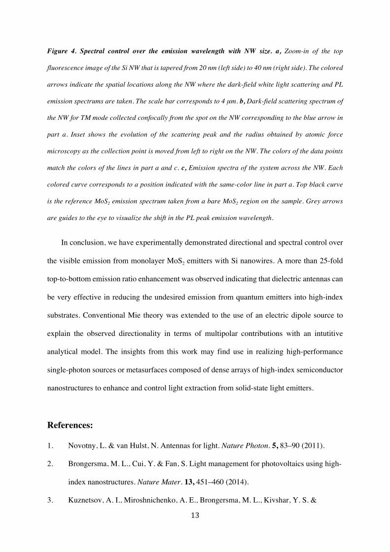
Figure 4. Spectral control over the emission wavelength with NW size. a, Zoom-in of the top
fluorescence image of the Si NW that is tapered from 20 nm (left side) to 40 nm (right side). The colored
arrows indicate the spatial locations along the NW where the dark-field white light scattering and PL
emission spectrums are taken. The scale bar corresponds to 4 μm. b, Dark-field scattering spectrum of
the NW for TM mode collected confocally from the spot on the NW corresponding to the blue arrow in
part a. Inset shows the evolution of the scattering peak and the radius obtained by atomic force
microscopy as the collection point is moved from left to right on the NW. The colors of the data points
match the colors of the lines in part a and c. c, Emission spectra of the system across the NW. Each
colored curve corresponds to a position indicated with the same-color line in part a. Top black curve
is the reference MoS2 emission spectrum taken from a bare MoS2 region on the sample. Grey arrows
are guides to the eye to visualize the shift in the PL peak emission wavelength.
In conclusion, we have experimentally demonstrated directional and spectral control over
the visible emission from monolayer MoS2 emitters with Si nanowires. A more than 25-fold
top-to-bottom emission ratio enhancement was observed indicating that dielectric antennas can
be very effective in reducing the undesired emission from quantum emitters into high-index
substrates. Conventional Mie theory was extended to the use of an electric dipole source to
explain the observed directionality in terms of multipolar contributions with an intutitive
analytical model. The insights from this work may find use in realizing high-performance
single-photon sources or metasurfaces composed of dense arrays of high-index semiconductor
nanostructures to enhance and control light extraction from solid-state light emitters.
References:
1. Novotny, L. & van Hulst, N. Antennas for light. Nature Photon. 5, 83–90 (2011).
2. Brongersma, M. L., Cui, Y. & Fan, S. Light management for photovoltaics using high-
index nanostructures. Nature Mater. 13, 451–460 (2014).
3. Kuznetsov, A. I., Miroshnichenko, A. E., Brongersma, M. L., Kivshar, Y. S. &

14
Lukyanchuk, B. Optically resonant dielectric nanostructures. Science 354, 846 (2016).
4. Cao, L. et al. Semiconductor nanowire optical antenna solar absorbers. Nano Lett. 10,
439–445 (2010).
5. Schuller, J., Zia, R., Taubner, T. & Brongersma, M. L. Dielectric metamaterials based
on electric and magnetic resonances of silicon carbide particles. Phys. Rev. Lett. 99,
107401 (2007).
6. Cao, L. et al. Engineering light absorption in semiconductor nanowire devices. Nature
Mater. 8, 643–647 (2009).
7. Cao, L., Park, J.-S., Fan, P., Clemens, B. & Brongersma, M. L. Resonant germanium
nanoantenna photodetectors. Nano Lett. 10, 1229–1233 (2010).
8. Jahani, S. & Jacob, Z. All-dielectric metamaterials. Nature Nanotech. 11, 23–36
(2016).
9. Groep, J. Van De & Polman, A. Designing dielectric resonators on substrates :
Combining magnetic and electric resonances. Opt. Express 21, 1253–1257 (2013).
10. Spinelli, P., Verschuuren, M. A. & Polman, A. Broadband omnidirectional
antireflection coating based on subwavelength surface Mie resonators. Nature
Commun. 3, 692 (2012).
11. Staude, I. et al. Shaping Photoluminescence Spectra with Magnetoelectric Resonances
in All-Dielectric Nanoparticles. ACS Photonics 2, 172–177 (2015).
12. Paniagua-Dominguez, R. et al. Generalized Brewster-Kerker effect in dielectric
metasurfaces. Nature Commun. 7, 10362 (2015).
13. Grzela, G. et al. Nanowire antenna emission. Nano Lett. 12, 5481–5486 (2012).
14. Paniagua-Domínguez, R., Grzela, G., Rivas, J. G. & Sánchez-Gil, J. A. Enhanced and
directional emission of semiconductor nanowires tailored through leaky/guided modes.
Nanoscale 5, 10582–10590 (2013).

15
15. Cao, L., Fan, P., Barnard, E. S., Brown, A. M. & Brongersma, M. L. Tuning the color
of silicon nanostructures. Nano Lett. 10, 2649–2654 (2010).
16. Staude, I. et al. Tailoring directional scattering through magnetic and electric
resonances in subwavelength silicon nanodisks. ACS Nano 7824–7832 (2013).
17. Sautter, J. et al. Active Tuning of All-Dielectric Metasurfaces. ACS Nano 4308–4315
(2015).
18. Person, S. et al. Demonstration of zero optical backscattering from single
nanoparticles. Nano Lett. 13, 1806–1809 (2013).
19. Kerker, M., Wang, D. & Giles, C. L. Electromagnetic scattering by magnetic spheres.
J. Opt. Soc. Am. 73, 765–767 (1983).
20. Geffrin, J. M. et al. Magnetic and electric coherence in forward- and back-scattered
electromagnetic waves by a single dielectric subwavelength sphere. Nature Commun.
3, 1171 (2012).
21. Fu, Y. H., Kuznetsov, A. I., Miroshnichenko, A. E., Yu, Y. F. & Luk’yanchuk, B.
Directional visible light scattering by silicon nanoparticles. Nature Commun. 4, 1527
(2013).
22. Wierer, J. J., David, A. & Megens, M. M. III-nitride photonic-crystal light-emitting
diodes with high extraction efficiency. Nature Photon. 3, 163–169 (2009).
23. Noda, S., Fujita, M. & Asano, T. Spontaneous-emission control by photonic crystals
and nanocavities. Nature Photon. 1, 449–458 (2007).
24. Fontana, Y., Grzela, G., Bakkers, E. P. A. M. & Rivas, J. G. Mapping the directional
emission of quasi-two-dimensional photonic crystals of semiconductor nanowires
using Fourier microscopy. Phys. Rev. B 86, 245303 (2012).
25. Kaniber, M. et al. Highly efficient single-photon emission from single quantum dots
within a two-dimensional photonic band-gap. Phys. Rev. B 77, 73312 (2008).

16
26. Peter, M. et al. Directional Emission from Dielectric Leaky-Wave Nanoantennas.
Nano Lett. 17, 4178–4183 (2017).
27. Chen, H. et al. Enhanced directional emission from monolayer WSe2 integrated onto a
multi-resonant silicon-based photonic structure. ACS Photonics (2017).
doi:10.1021/acsphotonics.7b00550
28. Curto, A. G. et al. Unidirectional emission of a quantum Ddot coupled to a
nanoantenna. Science 329, 930–933 (2010).
29. Kern, J. et al. Electrically driven optical antennas. Nature Photon. 9, 582–586 (2015).
30. Curto, A. G. et al. Multipolar radiation of quantum emitters with nanowire optical
antennas. Nature Commun. 4, 1750 (2013).
31. Hancu, I. M., Curto, A. G., Castro-López, M., Kuttge, M. & Van Hulst, N. F.
Multipolar interference for directed light emission. Nano Lett. 14, 166–171 (2014).
32. Liu, W., Miroshnichenko, A. E., Neshev, D. N. & Kivshar, Y. S. Broadband
unidirectional scattering by magneto-electric core-shell nanoparticles. ACS Nano
5489–5497 (2012).
33. Coenen, T., Bernal Arango, F., Femius Koenderink, A. & Polman, A. Directional
emission from a single plasmonic scatterer. Nature Commun. 5, 3250 (2014).
34. Tian, J., Li, Q., Yang, Y. & Qiu, M. Tailoring unidirectional angular radiation through
multipolar interference in a single-element subwavelength all-dielectric stair-like
nanoantenna. Nanoscale 8, 4047–4053 (2016).
35. Yang, Y., Li, Q. & Qiu, M. Controlling the angular radiation of single emitters using
dielectric patch nanoantennas. Appl. Phys. Lett. 107, 31109 (2015).
36. Sikdar, D., Cheng, W. & Premaratne, M. Optically resonant magneto-electric cubic
nanoantennas for ultra-directional light scattering. J. Appl. Phys. 117, 83101 (2015).
37. Rolly, B., Stout, B., Bidault, S. & Bonod, N. Crucial role of the emitter-particle

17
distance on the directivity of optical antennas. Opt. Lett. 36, 3368–3370 (2011).
38. Rolly, B., Stout, B. & Bonod, N. Boosting the directivity of optical antennas with
magnetic and electric dipolar resonant particles. Opt. Express 20, 1473–1478 (2012).
39. Filonov, D. S. et al. Experimental verification of the concept of all-dielectric
nanoantennas. Appl. Phys. Lett. 100, 201113 (2012).
40. Campione, S., Basilio, L. I., Warne, L. K. & Sinclair, M. B. Tailoring dielectric
resonator geometries for directional scattering and Huygens’ metasurfaces. Opt.
Express 23, 2293–2307 (2015).
41. García-Cámara, B. et al. All-optical nanometric switch based on the directional
scattering of semiconductor nanoparticles. J. Phys. Chem. C 119, 19558–19564
(2015).
42. Vynck, K. et al. All-dielectric rod-type metamaterials at optical frequencies. Phys.
Rev. Lett. 102, 133901 (2009).
43. Krasnok, A. E., Miroshnichenko, A. E., Belov, P. a & Kivshar, Y. S. All-dielectric
optical nanoantennas. Opt. Express 20, 20599–20604 (2012).
44. Liu, W., Zhang, J., Lei, B., Ma, H. & Xie, W. Ultra-directional forward scattering by
individual core-shell nanoparticles. Opt. Express 22, 16178–16187 (2014).
45. Huang, K. C. Y., Jun, Y. C., Seo, M. & Brongersma, M. L. Power flow from a dipole
emitter near an optical antenna. Opt. Express 19, 19084 (2011).
46. Albella, P., Shibanuma, T. & Maier, S. A. Switchable directional scattering of
electromagnetic radiation with subwavelength asymmetric silicon dimers. Sci. Rep. 5,
18322 (2015).
47. Rolly, B., Geffrin, J.-M., Abdeddaim, R., Stout, B. & Bonod, N. Controllable emission
of a dipolar source coupled with a magneto-dielectric resonant subwavelength
scatterer. Sci. Rep. 3, 3063 (2013).

18
48. Mak, K. F., Lee, C., Hone, J., Shan, J. & Heinz, T. F. Atomically thin MoS2: A new
direct-gap semiconductor. Phys. Rev. Lett. 105, 136805 (2010).
49. Lopez-Sanchez, O., Lembke, D., Kayci, M., Radenovic, A. & Kis, A. Ultrasensitive
photodetectors based on monolayer MoS2. Nature Nanotech. 8, 497–501 (2013).
50. Wu, S. et al. Monolayer semiconductor nanocavity lasers with ultralow thresholds.
Nature 520, 69–72 (2015).
51. Akhavan, S., Cihan, A. F., Bozok, B. & Demir, H. V. Nanocrystal skins with exciton
funneling for photosensing. Small 10, 2470–2475 (2014).
52. Splendiani, A. et al. Emerging photoluminescence in monolayer MoS2. Nano Lett. 10,
1271–1275 (2010).
53. Coleman, J. N. et al. Two-dimensional nanosheets produced by liquid exfoliation of
layered materials. Science 331, 568–571 (2011).
54. Xia, F., Wang, H., Xiao, D., Dubey, M. & Ramasubramaniam, A. Two-dimensional
material nanophotonics. Nature Photon. 8, 899–907 (2014).
55. Sun, Z., Martinez, A. & Wang, F. Optical modulators with 2D layered materials.
Nature Photon. 10, 227–238 (2016).
56. Mak, K. F. & Shan, J. Photonics and optoelectronics of 2D semiconductor transition
metal dichalcogenides. Nature Photon. 10, 216–226 (2016).
57. Bohren, C. F. & Huffman, D. R. Absorption and Scattering of Light by Small
Particles. (Wiley, 1983).
58. Balanis, C. A. Advanced Engineering Electromagnetics. (Wiley, 1989).
59. Bharadwaj, P., Deutsch, B. & Novotny, L. Optical Antennas. Adv. Opt. Photonics 1,
438–483 (2009).
60. Ringler, M. et al. Shaping emission spectra of fluorescent molecules with single
plasmonic nanoresonators. Phys. Rev. Lett. 100, 203002 (2008).

19
61. Cui, Y., Lauhon, L. J., Gudiksen, M. S., Wang, J. & Lieber, C. M. Diameter-controlled
synthesis of single-crystal silicon nanowires. Appl. Phys. Lett. 78, 2214–2216 (2001).

20
Methods
Sample Preparation and NW properties. The tapered NW discussed in Figs. 2-4 with the
radius in the range of 20-40 nm, was grown in-house by a gold-catalyzed chemical vapor
deposition technique.6,61 The second NW of this study, NW2 with a radius of 88 nm was
purchased from Sigma-Aldrich Co. MoS2 monolayer samples with semi-continuous areas,
grown by chemical vapor deposition, were purchased from 2D Semiconductors Inc. The
granularity of PL maps in the paper is due to this imperfect surface coverage of MoS2. The
NWs were drop-casted on these MoS2 samples from a colloidal suspension.
MoS2 layer etching process. In order to eliminate the collection of emission from the MoS2
areas that are not optically coupled the NWs, we expose the sample to a mild Ar-plasma etching
process for 10 seconds in a sputtering system (AJA International Inc.). The NWs themselves
serve as a shadow mask protecting the emitter layer underneath while the rest of the MoS2
monolayer is removed.
Photoluminescence imaging and spectroscopy. Experiments were conducted on a modified
confocal microscope with top and bottom detection capabilities (Witec Alpha 300). The sample
was excited with 633 nm continuous-wave laser through the top objective. The top detection
path consists of an objective (Zeiss 100X, NA: 0.95), a linear polarizer, a laser filter (long-pass
with 650 nm cutoff), a fiber with a 20 μm core diameter serving as the confocal pinhole and a
fiber-coupled avalanche photo-diode (Micro Photon Devices (MPD)). The bottom detection
path consists of an objective (Zeiss 50X, NA: 0.55), a linear polarizer, a laser filter (long-pass
with 650 nm cutoff), and a free-space coupled avalanche photo-diode (MPD). The top objective
was chosen to have a high numerical aperture (NA) to increase the excitation resolution of the
system. The bottom objective, on the other hand, was a long working distance objective to
21
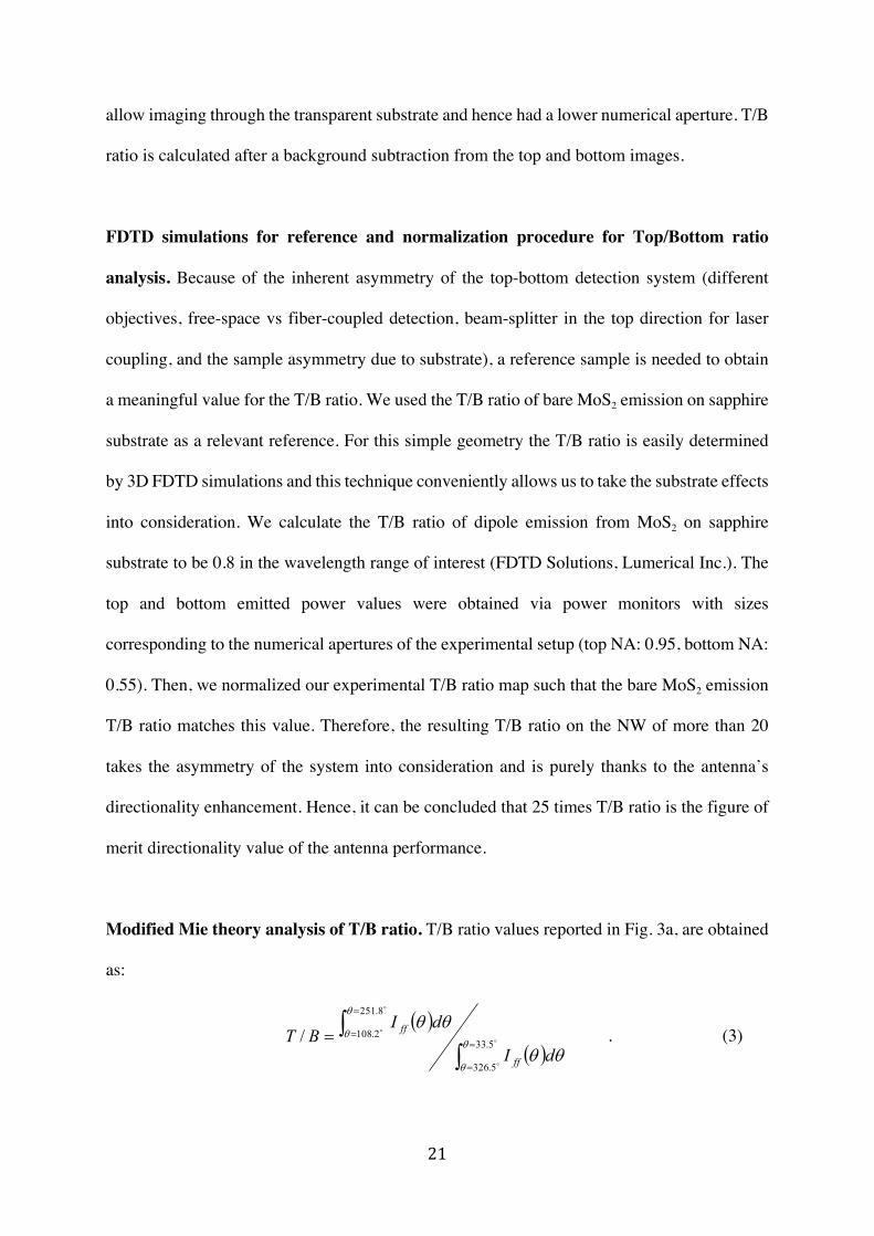
allow imaging through the transparent substrate and hence had a lower numerical aperture. T/B
ratio is calculated after a background subtraction from the top and bottom images.
FDTD simulations for reference and normalization procedure for Top/Bottom ratio
analysis. Because of the inherent asymmetry of the top-bottom detection system (different
objectives, free-space vs fiber-coupled detection, beam-splitter in the top direction for laser
coupling, and the sample asymmetry due to substrate), a reference sample is needed to obtain
a meaningful value for the T/B ratio. We used the T/B ratio of bare MoS2 emission on sapphire
substrate as a relevant reference. For this simple geometry the T/B ratio is easily determined
by 3D FDTD simulations and this technique conveniently allows us to take the substrate effects
into consideration. We calculate the T/B ratio of dipole emission from MoS2 on sapphire
substrate to be 0.8 in the wavelength range of interest (FDTD Solutions, Lumerical Inc.). The
top and bottom emitted power values were obtained via power monitors with sizes
corresponding to the numerical apertures of the experimental setup (top NA: 0.95, bottom NA:
0.55). Then, we normalized our experimental T/B ratio map such that the bare MoS2 emission
T/B ratio matches this value. Therefore, the resulting T/B ratio on the NW of more than 20
takes the asymmetry of the system into consideration and is purely thanks to the antenna’s
directionality enhancement. Hence, it can be concluded that 25 times T/B ratio is the figure of
merit directionality value of the antenna performance.
Modified Mie theory analysis of T/B ratio. T/B ratio values reported in Fig. 3a, are obtained
as:
( )( )ò
ò=
=
=
== !
!
!
!
5.33
5.326
8.251
2.108/ q
q
q
q
dI
dIBT
ff
ff . (3)
22
The integration limits were determined such that the calculated values correspond to the
experiments with the correct numerical apertures: top NA = 0.95 and bottom NA = 0.55. Note
that this calculation is for the emitter-antenna system in free-space without a substrate. In order
to confirm that the presence of the substrate is insignificant, we obtained the same parameter
sweep result of T/B ratio from FDTD simulations with a sapphire substrate (see Supplementary
Fig. S4). The comparison between the FDTD result involving the substrate (Fig. S4) and the
analytical result (Fig. 3a) shows that the presence of the substrate is indeed not critical for the
directionality in this system.
The significantly higher T/B ratios in calculations (and simulations in Suppl. Info.) as
compared to experiments are expected as the calculations only consider the emission from one
source dipole placed directly underneath the NW at an optimized spacing. In experiments,
however, there will be a distribution of emitters from the MoS2 region underneath the NW,
which results in a deviation of the emitter-to-NW distance from the optimum.
To further verify the validity of the 2D model and the simulations reported in Suppl. Info.,
we also conducted a few exemplary 3D simulations showing the accuracy of the 2D modeling
of the considered system NW emitter system (see Figure S2).
Acknowledgements
This research was conducted with the support from Air Force Office of Scientific Research
(AFOSR) and support of the Quantum Metaphotonics and Metamaterials MURI (AFOSR
Award No. FA9550-12-1-0488) and Stanford Electrical Engineering Departmental Fellowship.
S.R. acknowledges support by a research grant (VKR023371) from VILLUM FONDEN.
A.G.C. acknowledges the support of a Marie Curie International Outgoing Fellowship.

23
Author contributions
A.F.C. and M.L.B. conceived the idea; A.F.C., A.G.C. and M.L.B. designed the experiments;
A.F.C. prepared the samples and carried out the experiments; S.R. conducted the theoretical
calculations; A.F.C. conducted full-field simulations. P.K. provided guidance at the
simulations and experiments. All authors analyzed and discussed the results and were involved
in writing the manuscript.

24
Supplementary Information
Silicon Nanoantennas for Highly Directional Light Emission from monolayer MoS2
Ahmet Fatih Cihan1, Alberto G. Curto1,2, Søren Raza1, Pieter G. Kik1,3
and Mark L. Brongersma1
4. Geballe Laboratory for Advanced Materials, Stanford University, Stanford, California 94305, United States
5. Dep. Applied Physics and Institute for Photonic Integration, Eindhoven University of Technology, 5600 MB Eindhoven, The Netherlands
6. CREOL, The College of Optics and Photonics, University of Central Florida, Florida 32816, United States
*Corresponding Author: [email protected]
This supplementary information consists of 6 sections in support of the main body of the
text. The contents of the sections are listed below:
S1. Comparison of Plane Wave Excitation to Far-Away Dipole Excitation
S2. Derivation of Scattering Efficiency of a Nanowire under Dipole Excitation
S3. Derivation of Far-Field Radiation Patterns
S4. Comparison of Radiation Patterns for 2D and 3D Simulations
S5. Top and Bottom Fluorescence Image Cross-Sections for NW1
S6. FDTD Simulations of T/B Ratio

25
Section S1: Comparison of Plane Wave Excitation to Distant Dipole Excitation
Figure S1. Scattering from a Si nanowire (NW) for plane wave and distant dipole sources. a,
Schematic of the NW under plane wave excitation. b, Scattering efficiency, Qscat, and the modal
contributions from the electric dipole, p, magnetic dipole, m, and electric quadrupole, qe, under plane
wave excitation for a NW with 70 nm radius. c, Schematic of the dipole-NW system with dipole-to-NW
distance of 2 μm. d, Scattering efficiency and the modal contributions for the dipole case in part c.
We compare the scattering behaviors of a Si nanowire (NW) under plane wave and dipole
excitations in Fig. S1. When the dipole-to-NW distance is much larger than the excitation
wavelength, we find that the spectral dependences of the scattering efficiencies become
identical. However, the amplitude of the scattering efficiency is much lower in the dipole case
because the NW is far away from the source, allowing only a small fraction of the emitted light
to excite the multipolar resonances of the NW.
26
Section S2: Derivation of Scattering Efficiency of a Nanowire under Dipole Excitation
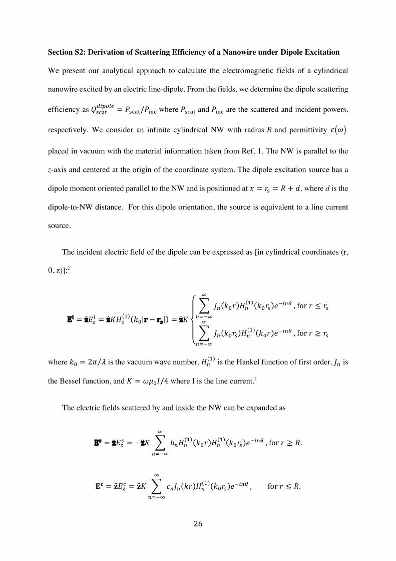
We present our analytical approach to calculate the electromagnetic fields of a cylindrical
nanowire excited by an electric line-dipole. From the fields, we determine the dipole scattering
efficiency as 𝑄"#$%\Z]^_` = 𝑃"#$%/𝑃'D# where 𝑃"#$% and 𝑃'D# are the scattered and incident powers,
respectively. We consider an infinite cylindrical NW with radius 𝑅 and permittivity
placed in vacuum with the material information taken from Ref. 1. The NW is parallel to the
z-axis and centered at the origin of the coordinate system. The dipole excitation source has a
dipole moment oriented parallel to the NW and is positioned at 𝑥 = 𝑟" = 𝑅 + 𝑑, where d is the
dipole-to-NW distance. For this dipole orientation, the source is equivalent to a line current
source.
The incident electric field of the dipole can be expressed as [in cylindrical coordinates (r,
θ, z)]:2
Ei = z𝐸gZ = z𝐾𝐻:8 𝑘: r − rs = z𝐾
𝐽5 𝑘:𝑟 𝐻58 𝑘:𝑟k 𝑒AZ5[
?
5@A?
,for𝑟 ≤ 𝑟k
𝐽5 𝑘:𝑟k 𝐻58 𝑘:𝑟 𝑒AZ5[
?
5@A?
,for𝑟 ≥ 𝑟k
where 𝑘: = 2𝜋 𝜆 is the vacuum wave number, 𝐻58 is the Hankel function of first order, 𝐽5 is
the Bessel function, and 𝐾 = 𝜔𝜇:𝐼/4 where I is the line current.2
The electric fields scattered by and inside the NW can be expanded as
Es = z𝐸gk = −z𝐾 𝑏5𝐻58 𝑘:𝑟 𝐻5
8 𝑘:𝑟k 𝑒AZ5[?
5@A?
,for𝑟 ≥ 𝑅.
𝐄𝐜 = 𝐳𝐸gx = 𝐳𝐾 𝑐5𝐽5 𝑘𝑟 𝐻58 𝑘:𝑟k 𝑒AZ5[
?
5@A?
, for𝑟 ≤ 𝑅.
ε ω( )

27
respectively, where k = k0 ε ω( ) is the wave number in the NW. Applying Maxwell’s
boundary conditions at the surface of the NW determines the expansion coefficients 𝑏5 and 𝑐5.
We find 𝑏5 to be the conventional Mie coefficient also found in the case of plane-wave
excitation 3
𝑏5 =𝐽5 𝑘𝑅 𝐽5z 𝑘:𝑅 − 𝜀(𝜔)𝐽5 𝑘:𝑅 𝐽5z 𝑘𝑅
𝐽5 𝑘𝑅 𝐻5(8)z 𝑘:𝑅 − 𝜀(𝜔)𝐻5
(8) 𝑘:𝑅 𝐽5z 𝑘𝑅.
Now that we have the scattered and incident electric fields, we can calculate the scattered
and incident powers:4
𝑃"#$% = 𝑅 d𝜃𝐒𝐬𝐜𝐚𝐭(𝑟 = 𝑅, 𝜃) ∙ 𝐫6S
:
,
where 𝐒𝐬𝐜𝐚𝐭 ∙ 𝐫 is the radial component of the Poynting vector associated with scattered
fields. 𝐒𝐬𝐜𝐚𝐭 =86𝑅𝑒 𝐄𝐬×𝐇𝐬∗ . After some straightforward but lengthy algebra we arrive at the
result
𝑃"#$% =18𝜔𝜇:𝐼
6 𝑏5 6 𝐻58 𝑘: 𝑅 + 𝑑
6?
5@A?
.
Similarly, the incident power can be derived as
𝑃'D# =18𝜔𝜇:𝐼
6.
Therefore, the scattering efficiency is
𝑄"#$%&'()*+ =
𝑃"#$%𝑃'D#
= 𝑏5 6 𝐻58 𝑘: 𝑅 + 𝑑
6?
5@A?
.

28
For comparison, we add that the scattering efficiency for the plane wave case is
𝑄"#$%(*$D+A�$�+ =
2𝑘:𝑅
𝑏5 6?
5@A?
which is independent of the source position unlike the dipole case.
Section S3: Derivation of Far-Field Radiation Patterns
To derive the far-field radiation pattern, we must examine the equations for the incident and
scattered field for large distance 𝑟. Utilizing the asymptotic relations for the Hankel functions
of first order
lim�P�→?
𝐻58 𝑘:𝑟 = 6
S(−𝑖)5𝑒AZS/� `
��P�
�P�,
we determine the incident and scattered far-fields as
lim�P�→∞
Ei = z𝐾2𝜋 𝑒
AZS/� −𝑖 5𝐽5(𝑘:𝑟k)𝑒AZ5[𝑒Z�P�
𝑘:𝑟
∞
5@A∞
≡ Effi (𝜃)𝑒Z�P�
𝑘:𝑟
lim�P�→?
Es = −z𝐾2𝜋 𝑒
AZS/� −𝑖 5𝑏5𝐻5(8)(𝑘:𝑟k)𝑒AZ5[
𝑒Z�P�
𝑘:𝑟
?
5@A?
≡ Effs 𝜃𝑒Z�P�
𝑘:𝑟.
Hence, the total electric far-field is
Efft 𝜃 = Effi 𝜃 + Effs 𝜃 = z𝐾2𝜋 𝑒
AZS/� −𝑖 5 𝐽5 𝑘:𝑟k − 𝑏5𝐻58 𝑘:𝑟k ,
?
5@A?
and the far-field intensity becomes:
IKK 𝜃 = 𝐄𝐟𝐟𝐭 𝜃 6 =18𝜋𝜔
6𝜇:6𝐼6 −𝑖 5𝑒AZ5[ 𝐽5 𝑘:𝑟k − 𝑏5𝐻58 𝑘:𝑟k
?
5@A?
6
.
29
Section S4: Comparison of Radiation Patterns for 2D and 3D Simulations
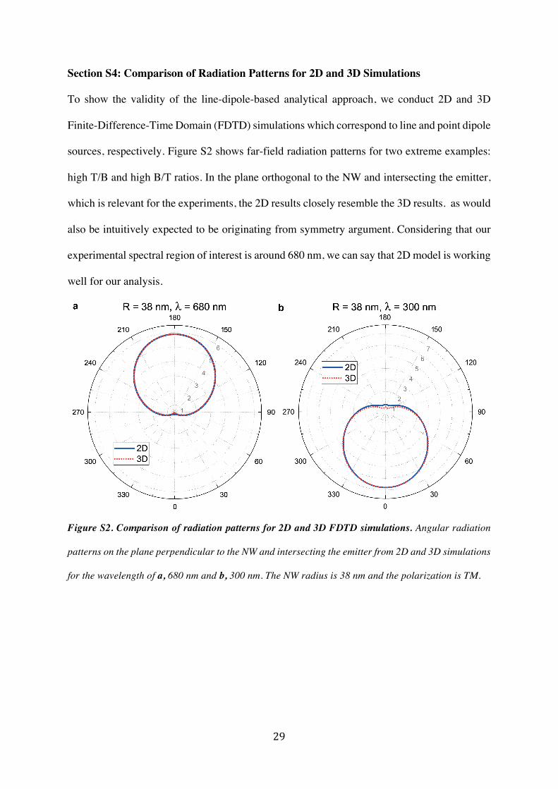
To show the validity of the line-dipole-based analytical approach, we conduct 2D and 3D
Finite-Difference-Time Domain (FDTD) simulations which correspond to line and point dipole
sources, respectively. Figure S2 shows far-field radiation patterns for two extreme examples:
high T/B and high B/T ratios. In the plane orthogonal to the NW and intersecting the emitter,
which is relevant for the experiments, the 2D results closely resemble the 3D results. as would
also be intuitively expected to be originating from symmetry argument. Considering that our
experimental spectral region of interest is around 680 nm, we can say that 2D model is working
well for our analysis.
Figure S2. Comparison of radiation patterns for 2D and 3D FDTD simulations. Angular radiation
patterns on the plane perpendicular to the NW and intersecting the emitter from 2D and 3D simulations
for the wavelength of a, 680 nm and b, 300 nm. The NW radius is 38 nm and the polarization is TM.
30
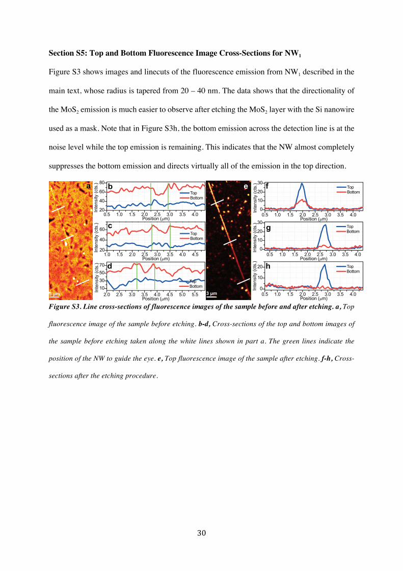
Section S5: Top and Bottom Fluorescence Image Cross-Sections for NW1
Figure S3 shows images and linecuts of the fluorescence emission from NW1 described in the
main text, whose radius is tapered from 20 – 40 nm. The data shows that the directionality of
the MoS2 emission is much easier to observe after etching the MoS2 layer with the Si nanowire
used as a mask. Note that in Figure S3h, the bottom emission across the detection line is at the
noise level while the top emission is remaining. This indicates that the NW almost completely
suppresses the bottom emission and directs virtually all of the emission in the top direction.
Figure S3. Line cross-sections of fluorescence images of the sample before and after etching. a, Top
fluorescence image of the sample before etching. b-d, Cross-sections of the top and bottom images of
the sample before etching taken along the white lines shown in part a. The green lines indicate the
position of the NW to guide the eye. e, Top fluorescence image of the sample after etching. f-h, Cross-
sections after the etching procedure.
e
3 μm
b
c
d
f
g
h
a
3 μm

31
Section S6: FDTD Simulations of T/B Ratio
In order to further verify the validity of our modified Mie theory approach, we conducted a
series of Finite Difference Time Domain (FDTD) simulations. In these 2D full-field
simulations we also included the sapphire substrate to check the validity of the analytical result
reported in Fig. 3a of the main text. Since the T/B ratio result shown in Fig. S4 is consistent
with Fig. 3a, we can say that the substrate has negligible impact on the directionality behavior
of our emitter-antenna system.
Figure S4. Numerical confirmation of the validity of modified Mie theory approach. T/B ratio
obtained with 2D FDTD simulations. The simulated structure includes a sapphire substrate and the T/B
ratio is obtained via power monitors whose sizes are determined based on the experimental numerical
apertures (0.95 for top and 0.55 for bottom).
Section S7: Supplementary References
1. Palik, E. D. Handbook of Optical Constants of Solids. (Academic Press, 1985). 2. Balanis, C. A. Advanced Engineering Electromagnetics. (Wiley, 1989). 3. Bohren, C. F. & Huffman, D. R. Absorption and Scattering of Light by Small
Particles. (Wiley, 1983). 4. Huang, K. C. Y., Jun, Y. C., Seo, M. & Brongersma, M. L. Power flow from a dipole
emitter near an optical antenna. Opt. Express 19, 19084 (2011).


![MIE Introduction [Demo]](https://static.fdocuments.in/doc/165x107/55a21c041a28ab7d5d8b470c/mie-introduction-demo.jpg)