Silicon DRIE vs. Germanium DRIE A Comparison in the ... DRIE... · Ge R9 PR: 5um gap 67um,...
22
CNF TCN, page 1 Silicon DRIE vs. Germanium DRIE A Comparison in the Plasmatherm VLN Vince Genova CNF Research Staff NNCI Etch Workshop Cornell University 5/24/2016 The Cornell NanoScale Science & Technology Facility
Transcript of Silicon DRIE vs. Germanium DRIE A Comparison in the ... DRIE... · Ge R9 PR: 5um gap 67um,...

CNF TCN, page 1
Silicon DRIE vs. Germanium DRIE
A Comparison in the Plasmatherm VLN
Vince Genova
CNF Research Staff
NNCI Etch Workshop
Cornell University
5/24/2016
The Cornell NanoScale Science & Technology Facility

CNF TCN, page 2
What do we know about Si and Ge etching in fluorine?
• Si-Si bonds are stronger than Ge-Ge bonds
• Ge is more easily oxidized than silicon
• Ge native oxide thickness is 4X that of silicon’s native oxide
• Ge-O bond (3.66eV) is weaker than Si-O bond (4.82eV)
• Ge affinity to oxygen is much greater than silicon’s affinity to oxygen
• Ge affinity to oxygen is much greater than its affinity to fluorine
• The thermal conductivity of silicon is 2X that of germanium
• Both Si and Ge react spontaneously with fluorine in the absence of ion bombardment
• SiF4 and GeF4 are the principal reaction products in fluorine based plasmas
• GeF4 is somewhat less volatile than SiF4 at typical etch temperatures
• In the case of SF6, GeS is less volatile than SiS
• Si etch rates are more strongly enhanced by ion bombardment than Ge
• Si and Ge reactions with halogens are exothermic
• Si-halogen bonds are stronger than Ge-halogen bonds
• Lower activation energy is needed for Ge fluorine based etching (not for Cl or Br)
• Etch rates are primarily determined by substrate reactivity and reaction product removal

CNF TCN, page 3
More specifics of Si and Ge etching in SF6/C4F8 based plasmas
• DC biases in SF6 plasmas tend to be low
• Etching is largely done by radicals
• Ions play a less significant role
• Deposition of sulfur on Si or Ge is unlikely in pure SF6, more likely in fluorine deficient plasmas
• Reactive etch layer thicknesses up to 3ML are less on Ge (GeF2, GeF3..) than on silicon (2x)
• Deposition of carbon based polymer (CxFy) is less on Ge than Si (2x)
• CxFy polymer acts to limit the in-diffusion of F and the out diffusion of etch products
• Ge sidewalls have a less effective sidewall passivation
• Sidewall passivation reduces the sticking coefficient and reaction probability of fluorine creating a
Knudsen like diffusion of radicals down the feature sidewall
• Ge is affected more by ARDE due to reduction in neutral transport. (less sidewall passivation)
• SiOxFy inhibits etching while GeOxFy is more permeable to active species
• Removal of reaction products through the over layers is very important (Ge is thinner)
• Substrate surface plays a key role in etching
• Thermal conductivity or the lack thereof can influence surface mobility, reaction, and desorption

CNF TCN, page 4
PLASMATHERM VERSALINE DSE-Ge IAT DOE
DSEIII IAT DOE:
CONSTANTS:
C4F8=150
SF6=250
AR=30
DEP. PRESSURE=25mtorr
DEP. TIME=2sec
ETCHA PRESSURE=40mtorr
ETCHA TIME=1.5sec
ETCHB PRESSURE=60mtorr
ETCHB TIME=1.5sec
LOOPS=240
TIME=20 min.
FACTORS:
DEP. POWER: 1500, 1750, 2000W
ETCHA POWER: 1500, 1750, 2000W
ETCHB POWER: 2000, 2250, 2500W
VOLTAGE PEAK TO PEAK: 375, 400, 425V Ge Ge PR-ER Ge
um/min um/min nm/min 40um Si-ER Si-ER
RUN DEP.W EAW EBW VPP ER-40um ER-4um PR-ER SPR 40um 4um
1 1500 1500 2000 375 4.8 2.6 53 91 5.3 3.8
2 1500 1750 2250 400 6.5 3.4 86 76 5.4 3.8
3 1500 2000 2500 425 9.6 5.5 127 76 4.7 3.3
4 1750 1500 2500 400 6.1 3.3 72 85 5.5 3.9
5 1750 1750 2000 425 7.2 3.4 101 71 5.1 3.5
6 1750 2000 2250 375 6.8 3 105 65 4 3.1
7 2000 1500 2250 425 4.4 3.7 70 63 5.8 4
8 2000 1750 2500 375 7.9 4 88 90 5 3.5
9 2000 2000 2000 400 6.3 2.7 115 55 4.5 3.7

CNF TCN, page 5
0
1
2
3
4
5
6
7
8
1400 1500 1600 1700 1800 1900 2000 2100
ER(um/min)
DEP (W)
DRIE-DOE-DEP W-40u
Ge
Si

CNF TCN, page 6
0
1
2
3
4
5
6
7
8
1400 1500 1600 1700 1800 1900 2000 2100
ER(um/min)
ETCH A (W)
DRIE-DOE-ETCH A W-40u
Ge
Si

CNF TCN, page 7
0
1
2
3
4
5
6
7
8
9
1900 2000 2100 2200 2300 2400 2500 2600
ER(um/min)
ETCH B(W)
DRIE-DOE-EBW-40u
Ge
Si

CNF TCN, page 8
0
1
2
3
4
5
6
7
8
370 380 390 400 410 420 430
ER(um/min)
V P-P (V)
DRIE-DOE-VP-P 40u
Ge
Si

CNF TCN, page 9
0
0.5
1
1.5
2
2.5
3
3.5
4
1400 1500 1600 1700 1800 1900 2000 2100
ER(um/min)
DEP (W)
DRIE-DOE-DEP W-4um
Ge
Si

CNF TCN, page 10
0
0.5
1
1.5
2
2.5
3
3.5
4
1400 1500 1600 1700 1800 1900 2000 2100
ER(um/min)
EA(W)
DRIE DOE EA W-4um
Ge
Si

CNF TCN, page 11
0
0.5
1
1.5
2
2.5
3
3.5
4
4.5
5
1900 2000 2100 2200 2300 2400 2500 2600
ER(um/min)
EB (W)
DRIE DOE EB W-4um
Ge
Si
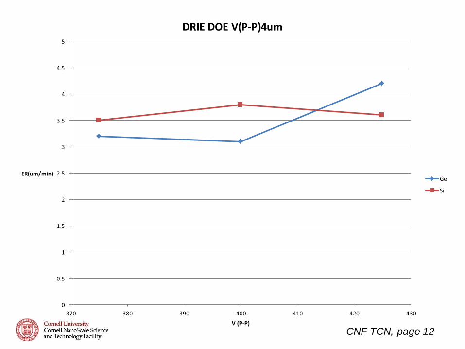
CNF TCN, page 12
0
0.5
1
1.5
2
2.5
3
3.5
4
4.5
5
370 380 390 400 410 420 430
ER(um/min)
V (P-P)
DRIE DOE V(P-P)4um
Ge
Si

CNF TCN, page 13
Si vs. Ge DRIE
Silicon-R5 PR: 40um gap 115um, 5.1u/min
4um gap 69um, 3.5u/min, AR=17:1
Ge:R5 PR:40um gap 144um, 7.2u/min
4um gap 60um, 3.4u/min, AR=15:1

CNF TCN, page 14
Si vs. Ge DRIE
Silicon R8 PR: 6.7um gap 74um, 3.7u/min
AR=11:1
Ge R8 PR: 6.7um gap 84um, 4.2um/min
AR=12:1

CNF TCN, page 15
Si vs. Ge DRIE
Si R9 PR: 5um gap 74um, 3.7u/min
AR=15:1
Ge R9 PR: 5um gap 67um, 3.4u/min,
AR=13.5:1

CNF TCN, page 16
Plasmatherm Versaline
Silicon DRIE
Si DRIE-IAT-AS200-PR mask
1um patterned on a 2um pitch
Si DRIE-IAT-AS200-PR mask
1um patterned300nm etched lines

CNF TCN, page 17
Plasmatherm Versaline
Silicon DRIE
Si DRIE-SiO2 mask
2.5um patterned lines, 86um deep, AR>34:1
Si DRIE-SiO2 mask-IAT
Actual etched linewidth=660nm

CNF TCN, page 18
Plasmatherm Versaline
Silicon DRIE
Si-700nm lines, 18um deep, 26:1 AR, 2.2u/min
ALD Al2O3 mask-15nm
Si-800nm lines, 18um deep, 23:1 AR, 2.2u/min
ALD Al2O3 mask-15nm

CNF TCN, page 19
Plasmatherm Versaline DRIE
Germanium
Ge DRIE: PR mask-GKR-ASML
R7-IAT DOE: 3.7um/min, 25:1 AR
Ge DRIE: SiO2 mask
R5-IAT DOE: 3.9um/min, 16:1 AR
CNF TCN, page 20
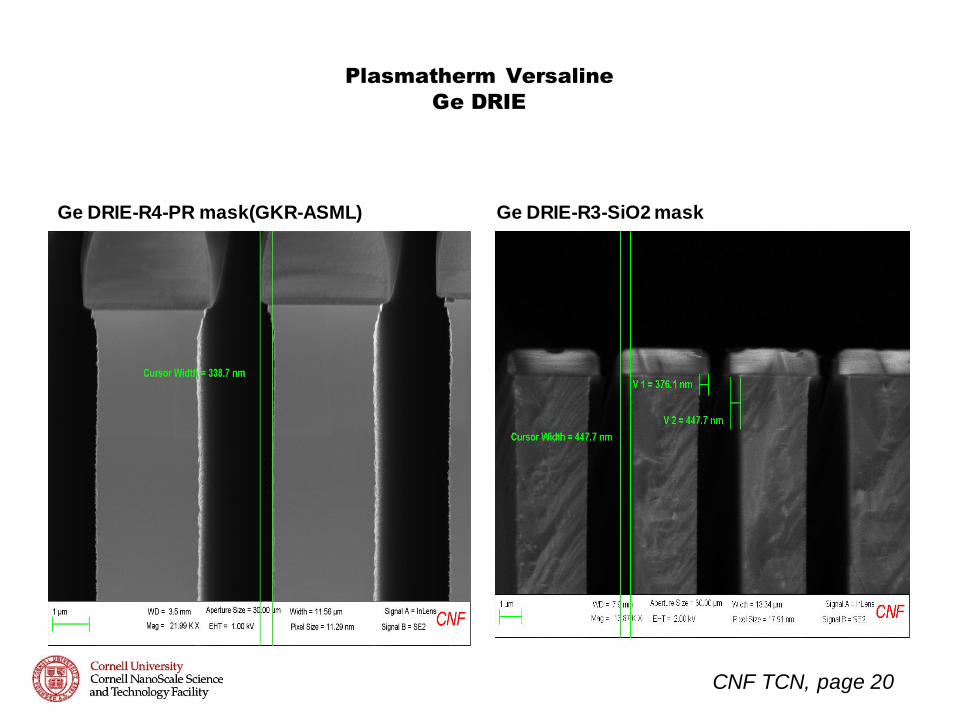
Plasmatherm Versaline
Ge DRIE
Ge DRIE-R4-PR mask(GKR-ASML)
Ge DRIE-R3-SiO2 mask

CNF TCN, page 21
Plasmatherm Versaline
Ge DRIE
Ge DRIE-Al2O3 mask (70nm)-R2
Minimal RIE lag
Ge-R1-Al2O3 mask: 3.5u gaps, 17:1 AR,
3u/min

CNF TCN, page 22
Conclusions
• Etch rates of Ge exceed Si for large features and aspect ratios<13:1
• Etch rates much closer for higher aspect ratios (>13:1) with Si having somewhat higher ERs.
• Ions play a more significant role in high aspect features enhancing Si ERs.
• Thinner reactive etch layer on Ge and its higher reactivity leads to generally higher ERs.
• Lower Ge thermal conductivity yields higher surface mobility, F substitution of O, & desorption.
• Increased heating during the Ge etch also leads to thinner surface polymer, less tapering..
• Higher oxygen concentration at the Ge interface can also mitigate polymer deposition.
• Thinner and more permeable sidewall inhibitor on the Ge perhaps leads to reduced scalloping and
a higher sticking coefficient of atomic F may also contribute to sidewall smoothing.