Sequence Generator - ece.umaine.edu
90
1 Sequence Generator Roman Shugayev Department of electrical and Computer Engineering University of Maine Orono, Maine [email protected] December 15, 2004
Transcript of Sequence Generator - ece.umaine.edu

1
Sequence Generator
Roman ShugayevDepartment of electrical and Computer Engineering
University of MaineOrono, Maine
December 15, 2004
2
Contents
1. Introduction 8
1.1 Project overview …………………………………………………..81.2 Objective …………………………………………………………..81.3 RFID tag architecture ……………………………………………..91.4 Digital Sequence Generator architecture…………………..…….111.5 Specifications…………………………………………………….121.6 Macros……………………………………………………………131.7 Pin-Out Assignment……………………………………………...131.8 Design Methodology……………………………………………..141.9 Known limitations of current design……………………………..14
2. Circuit design 15
2.1 Clock……………………………………………………………...152.1.1 T flip-flop…………………………………………...……...16
2.2 Shift register………………………………………...…………….172.2.1 D flip-flop……………………………………………...…...182.2.2 D latch…………………………………………………..….19
2.3 ROM……………………………………………..……………….20 2.4 Power supply………………………………………….………….21
2.4.1 StartFinish block………………………………….………..222.5 Delay block…………………………………….…………………232.6 Buffer…………………………………………………..…………242.7 Full circuit…………………………………………………..…….25

3
3. Circuit performance 27
3.1 Circuits simulations…………………………………………………273.1.1 Clock Simulation……………………………………………..273.1.2 T flip-flop simulation…………………………………………293.1.3 Shift register simulation………………………………………303.1.4 D flip-flop simulation………………………………………...313.1.5 D latch simulation…………………………………………….323.1.6 ROM simulation……………………………………………...333.1.7 Power supply simulation……………………………………..353.1.8 StartFinish block……………………………………………..363.1.9 Delay block simulations……………………………………...373.1.10 Buffer simulation…………………………………………….383.1.11 Full circuit simulation………………………………………..39
3.2 Current consumption………………………………………………..423.3 Performance vs. Temperature………………………………………433.4 Discussion of simulation results…………………………………….43
4. Physical Design 44
4.1 Description of components…………………………………………444.2 Layout considerations………………………………………………444.3 Floor planning………………………………………………………454.4 Component layout…………………………………………………..46
5. Verification 47
5.1 Introduction…………………………………………………………475.2 Design Rule Verification (DRC)……………………………………475.3 Layout versus Schematic check (LVS)……………………………..475.4 Simulation Results with included parasitics………………………..48
6. Experimental results 52
7. Conclusions 53
7.1 Summary of the Results…………………………………………….537.2 Future works………………………………………………………..537.3 Biography of the Author……………………………………………53

4
A Circuits-Schematics 55
B Circuits- Physical Design 76
5
List of tables
1.1 Sequence Generator specifications……………………………………..121.2 Table of Macros………………………………………………………..131.3 Table of Pin-Outs………………………………………………………13
4.1 Top level layout components…………………………………………..44

6
List of figures
1.1 RFID tag block diagram………………………………………………..10
2.1 Clock block schematic…………………………………………………152.2 T flip-flop schematic…………………………………………………...162.3 Shift register schematic………………………………………………...172.4 D flip-flop schematic…………………………………………………...182.5 D latch schematic………………………………………………………192.6 ROM block schematic………………………………………………….202.7 Power supply schematic………………………………………………..212.8 StartFinish block schematic……………………………………………222.9 Delay block schematic…………………………………………………232.10 Buffer schematic……………………………………………………...242.11 Full circuit schematic…………………………………………………26
3.1 Simulation results for the clock circuit…………………..…………….283.2 Simulation results for the T flip-flop circuit…………………………...293.3 Simulation results for the shift register circuit…………………………303.4 Simulation results for the D flip flop circuit…………………………...313.5 Simulation results for the D latch circuit………………………………323.6 Circuit arrangement for testing the ROM block....…………………….333.7 Simulation results for testing the ROM circuit………………………...343.8 Simulation results for the power supply circuit………………………..353.9 Simulation results for the StartFinish block…………………………...363.10 Simulation results for the Delay block……………………………….373.11 Simulation results for the Buffer circuit……………………………...383.12 Simulation results for the full circuit…………………………………393.13 Simulation results for the full circuit. First cycle…………………….403.14 Simulation results for the full circuit. Second cycle………………….413.15 Simulation results for the worst-case current consumption…………..42
4.1 Block diagram of the chip layout………………………………………45
5.1 Simulation of the top-level schematic with parasitics………………….495.2 Simulation of the top-level schematic with parasitics. First cycle……..505.3 Simulation of the top-level schematic with parasitics. Second cycle…..51

7
A.1 Final chip……………………………………………………………....56A.2 Test configuration for the top-level schematic………………………...57A.3 Top level schematic……………………………………………………58A.4 Clock block……………………………………………………………59A.5 Shift register…………………………………………………………...60A.6 ROM block…………………………………………………………….61A.7 Delay block…………………………………………………………….62A.8 Power supply block……………………………………………………63A.9 Start finish block………………………………………………………64A.10 Output Buffer………………………………………………………...65A.11 T flip-flop…………………………………………………………….66A.12 D flip-flop…………………………………………………………….67A.13 D latch………………………………………………………………..68A.14 Inverter……………………………………………………………….69A.15 2 input NAND gate…………………………………………………..70A.16 8 input NAND gate…………………………………………………..71A.17 2 input NOR gate…………………………………………………….72A.18 XOR gate…………………………………………………………….73A.19 Transmission gate……………………………………………………74A.20 Circuit arrangement for testing the ROM block……………………..75
B.1 Final chip layout………………………………………………………77B.2 Clock layout…………………………………………………………...78B.3 Shift register layout……………………………………………………79B.4 ROM layout…………………………………………………………...80B.5 Delay block layout…………………………………………………….81B.6 Power supply layout…………………………………………………..82B.7 Buffer layout…………………………………………………………..83B.8 Inverter layout…………………………………………………………84B.9 2 input NAND gate layout…………………………………………….85B.10 8 input NAND gate layout…………………………………………...86B.11 2 input NOR gate layout……………………………………………..87B.12 XOR layout…………………………………………………………..88B.13 Transmission gate layout…………………………………………….89

8
Chapter 1
Introduction
1.1Project overview
At this time there is an on-going research worldwide in the area of RFID(Radio frequency identification). This technology uses electromagnetic waves to detect and uniquely identify people and objects. RFID system consists of a tag-transmitter and a receiver. The receiver sends RF waves of the specified frequency which provide the transmitter the enable signal as well as required energy to power up the transmitter circuit. The transmitter sends an identification signal, which is picked up and analyzed by the receiver.The project being developed by the University of Maine department of Electrical Engineering has the goal of designing a viable RFID microchip. At this phase the work is primarily concentrated on the design and testing of separate RFID building blocks. The current project was designed to implement the functionality of one of these blocks, a Digital Sequence Generator.
1.2 Objective The objective of current project was to design a microchip that would be able to generate a 64 bit predefined digital sequence. The sequence had to be transmitted at least twice during one transmission cycle to provide a consistence check at the receiver. The start of the sequence had to be delayed in time from the enable signal based on the data in the predefined sequence. The external inputs to the chip were specified to be an Enable signal and the digital clock. The required outputs were the sequence data output and the transmit enable output. The circuit had to operate from the single 5V power supply.

9
1.3 RFID tag architecture
The RFID project currently being developed consists of 3 main blocks (see figure 1.1).
The first one, PLL, receives the signal from the transmitter and locks on its frequency. This frequency is then provided to the rest of the circuitry. This arrangement was decided to be most efficient since the frequency in this case is defined externally eliminating temperature frequency variations the local oscillators are prone to. The transmitter frequency for the current project was chosen to be sufficiently high, ft=320 MHz. Since the locking of the PLL to the transmitter frequency does not occur instantaneously, the PLL provides the enable signal to the rest of the circuitry indicating that lock in has occurred and the transmit sequence can be safely initiated. The PLL circuit has the following outputs: 320 MHz-frequency output, a 10 MHz-frequency output, 625 KHz clock output and an Enable output.
The second block is a Digital Sequence Generator. Whenever it receives the enable signal from the PLL block it starts the process that leads to the delayed 128-bit sequence appearing on the output. The 64-bit sequence is transmitted twice to provide a consistency check at the receiver block. The 64-bit sequence data and the duration of the delay are determined by the code stored in ROM located in the same block. The outputs of this block are the transmit enable output and the sequence data output. The delay requirement arises from the consideration for the multiple RFID tags, being used simultaneously and located closely together. When all of them are exited with 320 MHz transmitter wave, the PLL settling time for the tags are almost equal. Therefore these tags will start transmitting at the same time, which, due to the fact that they utilize the same bandwidth, will result in erroneous readings by the receiver. When the start of transmission is predictably delayed the receiver is able to receive the identification sequences at the different times opposed to being received simultaneously ensuring the correct reading.
The third block is a mixer. It receives a digital sequence from the Digital Sequence Generator and modulates it with the 10 MHz signal such that every bit corresponding to 1 contains 8 10 MHz frequency periods and every bit corresponding to 0 corresponds to a 5V DC level. Then this modulated signal is mixed with a 320 MHz carrier frequency provided by the PLL block and used as a final output.
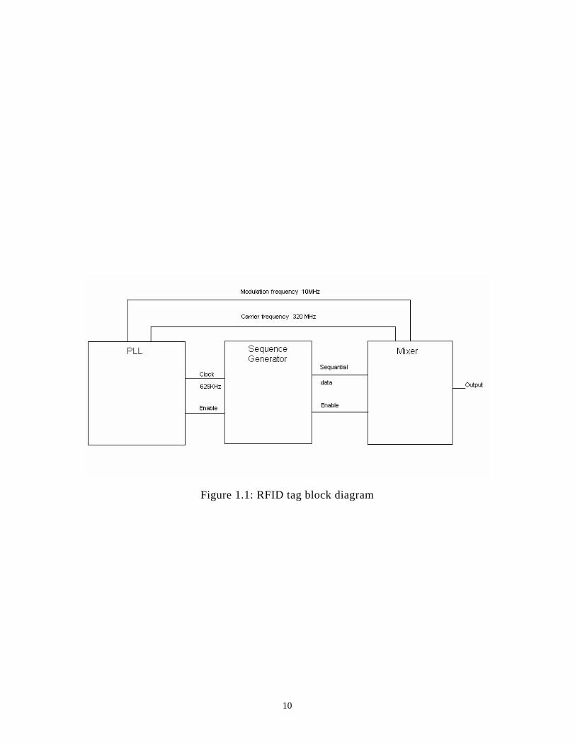
10
Figure 1.1: RFID tag block diagram
11
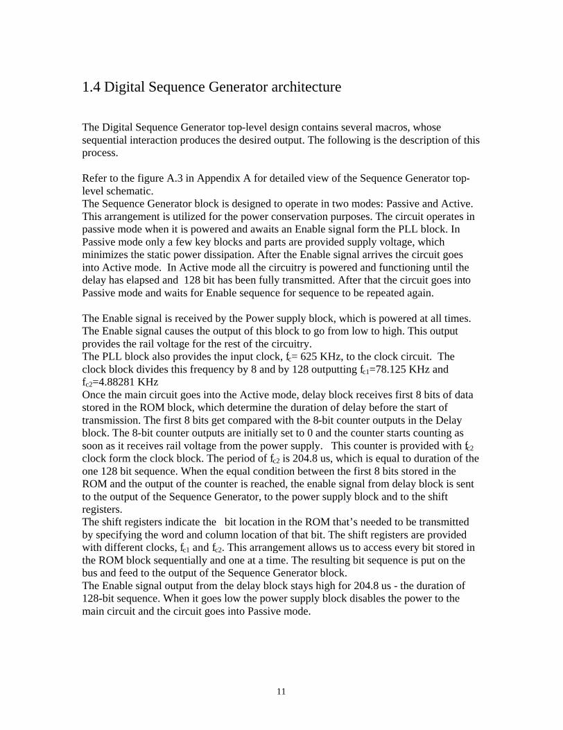
1.4 Digital Sequence Generator architecture
The Digital Sequence Generator top-level design contains several macros, whose sequential interaction produces the desired output. The following is the description of this process.
Refer to the figure A.3 in Appendix A for detailed view of the Sequence Generator top-level schematic. The Sequence Generator block is designed to operate in two modes: Passive and Active. This arrangement is utilized for the power conservation purposes. The circuit operates in passive mode when it is powered and awaits an Enable signal form the PLL block. In Passive mode only a few key blocks and parts are provided supply voltage, which minimizes the static power dissipation. After the Enable signal arrives the circuit goes into Active mode. In Active mode all the circuitry is powered and functioning until the delay has elapsed and 128 bit has been fully transmitted. After that the circuit goes into Passive mode and waits for Enable sequence for sequence to be repeated again.
The Enable signal is received by the Power supply block, which is powered at all times. The Enable signal causes the output of this block to go from low to high. This output provides the rail voltage for the rest of the circuitry. The PLL block also provides the input clock, fc= 625 KHz, to the clock circuit. The clock block divides this frequency by 8 and by 128 outputting fc1=78.125 KHz and fc2=4.88281 KHzOnce the main circuit goes into the Active mode, delay block receives first 8 bits of data stored in the ROM block, which determine the duration of delay before the start of transmission. The first 8 bits get compared with the 8-bit counter outputs in the Delay block. The 8-bit counter outputs are initially set to 0 and the counter starts counting as soon as it receives rail voltage from the power supply. This counter is provided with fc2
clock form the clock block. The period of fc2 is 204.8 us, which is equal to duration of the one 128 bit sequence. When the equal condition between the first 8 bits stored in the ROM and the output of the counter is reached, the enable signal from delay block is sent to the output of the Sequence Generator, to the power supply block and to the shift registers.The shift registers indicate the bit location in the ROM that’s needed to be transmitted by specifying the word and column location of that bit. The shift registers are provided with different clocks, fc1 and fc2. This arrangement allows us to access every bit stored in the ROM block sequentially and one at a time. The resulting bit sequence is put on the bus and feed to the output of the Sequence Generator block.The Enable signal output from the delay block stays high for 204.8 us - the duration of 128-bit sequence. When it goes low the power supply block disables the power to the main circuit and the circuit goes into Passive mode.

12
1.4 Specifications
Specifications UnitsTransmitted
sequence length 128 bit
Transmitted data 64 bit binary value 0100100001010101010100100101101001100101000111010101011110000000 -
Delay binary value 01000000 -
Delay actual value 409.6 us
Location of the starting bit in memory 2nd word, 2nd column -
Transmitted sequence duration 204.8 us
The number of unique sequences 1.84E+19 -
The number of unique delays 256 -
Receiver refresh rate 18 Hz
Current consumption in the passive mode 5 mA
Current consumption in the active mode 22 mA
Power consumption in the passive mode 25 mW
Power consumption in the active mode 110 mW
Table 1.1: Sequence Generator Specifications

13
1.6 Macros
Macros number Name1 Clock2 Shift register3 ROM4 Power supply5 Delay
Table 1.2: Table of Macros
Table 1.2 depicts the high level building blocks used in the current design. Note that the shift register block is utilized twice in the top-level schematic.
1.7 Pin-Out Assignment
Pin Number Function1 Vdd40 GND38 Clock input39 Enable input20 Digital sequence output21 Transmit enable output32 Test circuits clock33 Test Dff D input34 Test Tff T input35 Test TFF output37 Test Dff output
Table 1.3: Table of Pin-Outs
Table above indicates the pin assignment for the designed chip. The chip is powered using single 5V power supply. The same clock input signal is provided to all test circuits

14
1.8 Design Methodology
Our design consisted of the following steps:
1. Brainstorming2. Research, design draft3. Group discussion, corrections to the design draft4. Initial design, simulations5. Group discussion, corrections to the initial design6. Final design, simulations7. Layout, Design rules8. Tape out
1.9 Known limitations of current design
The major limitation of current design is the assumption that multiple RFID tags are located close to each other. However it could be different. Assuming that the transmitter signal is strong enough so 2 objects located 100 feet from each other are able to transmit the signal back to the receiver, and knowing that RF wave propagates with the speed of light we conclude that the enable signals received by these tags are going to be delayed in time by 0.1us. If these tags have a delay setting such that their transmission sequences follow each other continuously without the delay there is a possibility of overlap of two sequences. The possibility of erroneous reading is increasing with increasing distance.
Another limitation of the current design is a relatively low number of unique delays. It is set to 256 which, assuming modest size of the sample population, is ample, however it might be insufficient for the large scale applications.
Finally the delay solution implemented in the current design implies reduced receiver refresh rate which, assuming the worst case (256 uniquely delayed tags) is set to 18 Hz.However for most current applications of RFID technology this refresh rate is sufficient.

15
Chapter 2
Circuit design
This chapter discusses the concept and design of the top-level macros as well as the lower level design blocks. The desired performance of the chip can be achieved only by ensuring the predictable and correct performance of the individual blocks.The CMOS process has being used. The logic gates were designed to be minimum size and have equal rise and fall times.
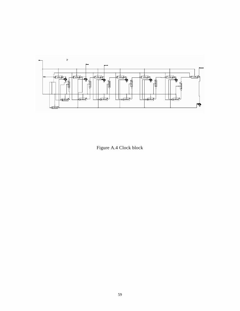
2.1 Clock
Figure 2.1: Clock Block Schematic
The frequency divider design (figure 2.1) was adopted from (1). The individual stages were implemented using T flip-flops. The intermediate circuitry uses AND gates and NOT gates. Significant modification of the current design was dictated by the power requirement. Every time the power supply block powers the circuit, we have to consider the initial conditions and the previous values of the frequency divider stages. Therefore the reset function was implemented by tying the outputs of the divider stages to ground through the NMOS transistors when the power is disabled.
The clock, fc=625 KHz is being feed from the PLL circuit. Every time the power is recycled the initial phase of the input clock becomes unknown, however this does not present any complication in our design, since all the clocks in the circuit are obtained by the frequency division of the input clock.
The outputs, fc1=78.125 KHz and fc2=4.88281 KHz are taken from the 3rd and 7th stage of the frequency divider.

16
2.1.1 T flip-flop
Figure 2.2: T flip-flop schematic
The design for T flip-flop (figure 2.2) was adopted form (1). Both Q and Qnot outputs of the D flip-flop, utilized in the designed occur simultaneously. The current design uses only NAND gates and NOT gates, opposed to the conventional design utilizing NAND and NOR gates.

17
2.2 Shift register
Figure 2.3: Shift register schematic
The shift register design (figure 2.3) was adopted and modified from (1). One of the peculiarities of our design was the requirement to have only one of the outputs, the output of the first stage, being tied high when the circuit is in Active mode but not yet transmitting. This is needed in order to set the first word high so the ROM circuit would be able to provide 8 bit of the first word to delay circuit that would determine the duration of the delay before the start of the transmission. The shift register is composed of 8 stages. Each stage consists of the D flip-flop and reset/ initiation circuit. The outputs of all the latches in the shift register block before the start of transmission are tied to ground except for the fist D-latch in the D flip-flop of the first stage, which is tied high. This arrangement insures that during the transmission cycle one and only one of the outputs would be high at any time.The output of the last stage is feed through transmission gate to the input of the first stage and the clock to D flip flops is provided through another transmission gate. The same Enable signal coming from the delay circuit enables the two transmission gates. Also, the first stage of the shift register is constantly powered to ensure the predictable behavior in case of power recycling and variable (in particular considering the case of 0 delay)The rest of the shift register circuitry is provided the rail voltage by the power supply block.
18
2.2.1 D flip-flop
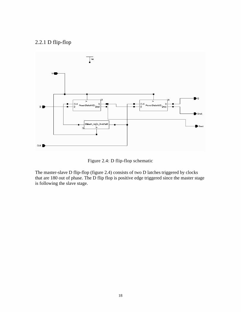
Figure 2.4: D flip-flop schematic
The master-slave D flip-flop (figure 2.4) consists of two D latches triggered by clocks that are 180 out of phase. The D flip flop is positive edge triggered since the master stage is following the slave stage.

19
2.2.2 D latch
Figure 2.5: D latch schematic
The design for D latch (figure 2.5) is adopted from (2). The main reason this design was chosen is the need for the counter in the Sequence Generator circuit. The ascending counter requires T flip-flops to be implemented. The T flip-flop requires the D flip-flop outputs Q and Q not to be simultaneous. This requirement is fulfilled by current design.

20
2.3 ROM
Figure 2.6: ROM block schematic
The circuit design from 1 has being used and modified (figure 2.6). The ROM block consists of 8*8 NMOS array with each bit data uniquely identified by word/column coordinates. When a word line goes high, columns in that particular word get selected one at a time by turning on the appropriate transmission gate and the content of that column appears on he bus line. The duration of the clock period corresponding to the word shift register is 8 times longer then that of the column shift register which allows us to capture all the data corresponding to a given word. By sequentially enabling word lines one at a time we are able to capture all the data stored in the ROM. The outputs to Delay circuit are taken directly as the column lines values bypassing the transmission gates.
21
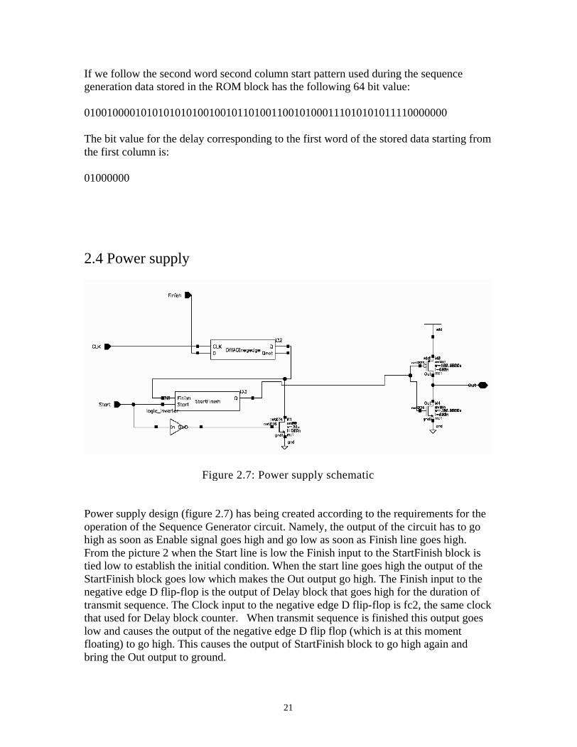
If we follow the second word second column start pattern used during the sequence generation data stored in the ROM block has the following 64 bit value:
0100100001010101010100100101101001100101000111010101011110000000
The bit value for the delay corresponding to the first word of the stored data starting from the first column is:
01000000
2.4 Power supply
Figure 2.7: Power supply schematic
Power supply design (figure 2.7) has being created according to the requirements for the operation of the Sequence Generator circuit. Namely, the output of the circuit has to go high as soon as Enable signal goes high and go low as soon as Finish line goes high. From the picture 2 when the Start line is low the Finish input to the StartFinish block is tied low to establish the initial condition. When the start line goes high the output of the StartFinish block goes low which makes the Out output go high. The Finish input to the negative edge D flip-flop is the output of Delay block that goes high for the duration of transmit sequence. The Clock input to the negative edge D flip-flop is fc2, the same clock that used for Delay block counter. When transmit sequence is finished this output goes low and causes the output of the negative edge D flip flop (which is at this moment floating) to go high. This causes the output of StartFinish block to go high again and bring the Out output to ground.

22
2.4.1 StartFinish block
Figure 2.8 StartFinish block schematic
The StartFinish circuit (figure 2.8) was designed to implement the output toggle requirements of the Power supply block. The circuit is implemented using a T flip-flop, the T input of which is tied high allowing it to Toggle the output on the rising edge of the CLK input. When the Start input is low the out put is tied high through the PMOS transistor. The Finish input is low therefore the in2 input of the NAND gate is high. When the Start input goes high, the CLK input of the T flip-flip goes high which causes the output to switch state, which in turn causes the in2 of the NAND gate to go low. When the Finish input goes high, the in2 of the NAND gate goes high, which cause the CLK input to the T flip-flop to go high and the output switches states again. The desired operation can be achieved only if Enable signal stays on during the full transmission cycle.

23
2.5 Delay block
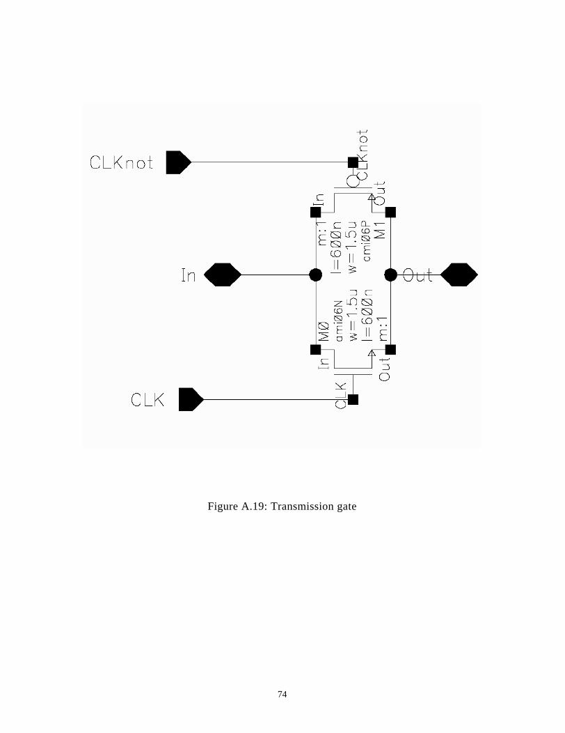
Figure 2.9: Delay block schematic
The Delay block (figure 2.9) produces the delayed enabled input based on the values of the inputs from the ROM block. The Delay block requires two input clocks: fc2 for the counter and fc for the comparator circuit. The reason the comparator circuit requires a clock is the inputs from the ROM block that are varying based upon what word is being active at any particular time. During the delay period, that is when the counter is counting, however the input values from the ROM and the values of the counter stage have not yet been matched, the first word in the ROM block is active ( see section 2.2 ) and the values of the bits in first word determine the duration of the delay. However, once the output of Delay circuit becomes high and the circuit starts transmitting, the words other then the first one become active as well. This operation changes the input values to Delay circuit and cause the output to go low, interrupting the transmission.
By latching the first word bit values we ensure uninterrupted transmission for the full duration of the transmission cycle. The latching is accomplished by utilizing the D flip-flops feed with fc clock through transmission gate.

24
The transmission gate is on during the delay period, however it gets disabled as soon asthe output of the Delay block goes high, latching the first word 8bit delay value in the D flip-flops. During the delay period this values as well as the state values of the 8 stages of the counter are feed to 8 XOR gates the output of which goes to 8 input NAND gate. This NAND gate provides the final output of Delay block.
2.6 Buffer
Figure 2.10: Buffer schematic
The buffer block (figure 2.10) was designed with the first stage small enough so it does not load the circuit outputs, yet large enough to be able to rapidly charge the second stage inverter. The number of stages was chosen to be even to preserve the logic output value. Because the fastest output frequency is not high, fc= 625 KHz the number of required stages was minimal.

25
2.7 Full circuit
The principal description of the Sequence Generator operation can be found in the Sequence Generator Architecture section. The design of the circuit (figure 2.11) was performed in stages based on the requirements for the circuit performance given at that moment. Therefore the circuit was initially designed to operate with the power constantly applied to it, and later modified to satisfy the power conservation requirements.In the Passive mode the following circuits are powered.
1. The Power Supply circuit. The reason this circuit provided with power is clear. The main circuit must have a certain part of it be powered at all times to be able to sense the Enable signal on the input and start the Sequence generation process.
2. The output buffers. Due to the large size of the transistors used in buffers, their on resistance will be fairly small and comparable with the resistance of the power supply switch. Therefore the voltage division between PMOS of the switch transistor and the PMOS of the buffer will result in reduction of the rail voltage provided to the circuit in Active mode, which will jeopardize the circuit performance.
3. The D flip-flops in the Shift Register blocks corresponding to output 1. The reason they were provided power was to ensure stable sequential propagation of bit 1 through the shift register ring as well as output 1of the shift registers being tied high during the delay period.
4. The Delay block enables signal inverter. It had to be powered to ensure the reset of the Delay block when the power to this Block goes off.
The clock signal of 4.88281 KHz frequency from the clock block to the power supply block had to be delayed and inverted so that the negative edge triggered D flip flop in the Power supply block will latch the value of output of the Delay block synchronously and be able to make the transition to Passive mode. The 78.125 KHz output of the clock block had to be inverted before it was feed to the shift register since the enable signal that appears on the output of the Delay block corresponds to the word and column clock being 180 degrees out of phase. To make them to be in phase and have them be high during the transition from low to high on the output of Delay the inverter was placed between the 78.125 KHz output of the clock block and the input of the word shift register.

26
Figure 2.11: Full circuit schematic

27
Chapter 3
Circuit performance
In this project performance of the separate blocks and full Sequence Generator circuit was analyzed. The simulations in this chapter were performed on the schematic level not taking into account the parasitic capacitances. The full simulation can be found in Chapter 5. No performance degradation was observed when performing a full simulation. The time limitations did not allow the simulation of the entire chip to be executed. Therefore the full simulation, although accounted for parasitic capacitances, did not consider the packaging parameters.
3.1 Circuits simulations
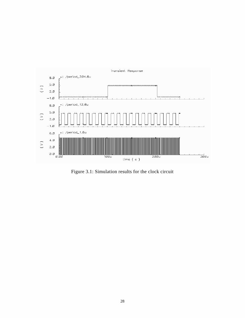
3.1.1 Clock Simulation
The clock circuit was simulated with a 625 KHz (1.6us period) input clock (figure 3.1). The frequency devisions by 8 and by 128 were performed successfully. The desired 78.125 KHz (12.8us) and 4.88281 KHz (204.8us) frequencies were obtained. The input and output waveforms for the clock simulation are shown on picture
28
Figure 3.1: Simulation results for the clock circuit

29
3.1.2 T flip-flop simulation
T flip-flop was simulated with a 100 MHz clock to test for latency as well as logical consistency (figure 3.2). The T input signal was chosen to be running off phase at 50 MHz the frequency twice that of the input clock. Below the clock was tied to net 5 and the T input signal for the T flip-flop was tied to net 3. The output of the T flip-flop, tied to the net 9, is toggled every time T flip-flop has 5 volts on the output on the rising edge of the clock and remains in the same state when there is 0 volts. The uncertainty about the initial condition is resolved in the top level blocks through the use of initiation circuits.
Figure 3.2: Simulation results for the T flip-flop circuit

30
3.1.3 Shift register simulation
Shift register block was simulated using delayed 625 KHz delayed clock (net 19) and delay 78.125 KHz enable signal (net 049) (figure 3.3). The durations of the delays were set equal. Net 60, net 58, net 9, net 8, net 54, net 6, net 50, net 4 represent the outputs of the shift register 1 through 8. It is clear form the graph that the desirable operation was achieved successfully. The outputs of the shift register turn high one at a time in a sequential order. The output 1 (net 60) is tied high whenever the enable signal is low. The rest of the outputs at that time are tied low. The first output that goes high when the input signal goes high is the output 2 (net 58) as given in specifications. A glitch occurring on the output 2 when the enable signal goes low will not affect the performance of the main circuit, since the power for the shift register blocks goes off as soon as enable signal goes low. (see Sequence Generator Architecture)
Figure 3.3: Simulation result for the shift register circuit
31
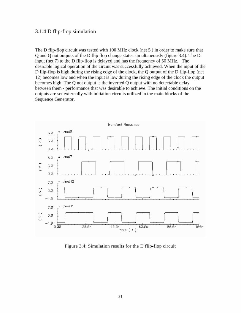
3.1.4 D flip-flop simulation
The D flip-flop circuit was tested with 100 MHz clock (net 5 ) in order to make sure that Q and Q not outputs of the D flip flop change states simultaneously (figure 3.4). The D input (net 7) to the D flip-flop is delayed and has the frequency of 50 MHz. The desirable logical operation of the circuit was successfully achieved. When the input of the D flip-flop is high during the rising edge of the clock, the Q output of the D flip-flop (net 12) becomes low and when the input is low during the rising edge of the clock the output becomes high. The Q not output is the inverted Q output with no detectable delay between them - performance that was desirable to achieve. The initial conditions on the outputs are set externally with initiation circuits utilized in the main blocks of the Sequence Generator.
Figure 3.4: Simulation results for the D flip-flop circuit

32
3.1.5 D latch simulation
The D latch circuit was tested with 100 MHz clock (net 7) to check for latency and logical consistency (figure 3.5). The input signal was delayed and had the same frequency as a clock signal. Opposed to the D flip-flop, the D latch is level sensitive therefore it changes state during the period of time when the clock input is high. Simulated outputs Q (net 12) and the inverted output Q not (net 11) are demonstrating the expected operation.
Figure 3.5: Simulation results for the D latch circuit

33
3.1.6 ROM simulation
The setup shown on Figure 3.6 was used to test the operation of ROM block. The ROM block (PowerROM block on the figure) was receiving the signals from the shift register (PowerShift_register on the figure). These signals were specifying column and word coordinates of the bit in the ROM block to be put on the output bus. The output sequence contained 64 bits of data stored in the ROM block One of the shift registers, providing the column inputs to the ROM, had a 625 KHz clock input (net7) and the other, providing a word input to the ROM had a 78.125 KHz input clock (net 3) as shown on Figure 3.7. Both shift registers were enabled with the same delayed enable signal with the frequency of 4.88281 KHz (net 5)The sequence, observed on the output of the ROM block (net 55) successfully corresponds to the stored data. The reproducibility of the output sequence was observed through the toggling of the enable signal. Net 16, net 17, net 18 and net 27, net 28, net 29 correspond to the shift registers outputs waveforms. By analyzing these results it’s easy to establish the start bit of the sequence which determined to be in accordance with specification as the second word second column bit.
Figure 3.6: Circuit arrangement for testing the ROM block

34
Figure 3.7: Simulation results for the ROM circuit

35
3.1.7 Power supply simulation
A clock signal with the frequency of 4.88281 KHz (net 1) was used to test the power supply block (figure 3.8). The Finish signal (net 3) is delayed, set initially high and has the frequency 2.44141 KHz. The Enable signal (net 5) has the frequency of 500 Hz. The desired performance of the circuit was obtained successfully. The output (net 12)goes high as soon as Enable signal goes high and goes low again when during the fallingedge of the clock the Finish signal is high.
Figure 3.8: Simulation results for the power supply circuit

36
3.1.8 StartFinish block
The StartFinish block was tested using a clock signal with the frequency of 4.88281 KHz (net 5) for the Start input and a delayed signal with the same frequency for the Finish input (net 3) as shown on Figure 3.9. The simulation performance was in line with expectations. The output (net 9) was initially tied high and would go low every time the Start signal would go high and then the output would go back high when the finish input would go high. The output would hold its state during the high to low transitions of the input signals.
Figure 3.9: Simulation results for the StartFinish block
37
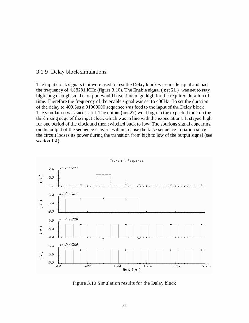
3.1.9 Delay block simulations
The input clock signals that were used to test the Delay block were made equal and had the frequency of 4.88281 KHz (figure 3.10). The Enable signal ( net 21 ) was set to stay high long enough so the output would have time to go high for the required duration of time. Therefore the frequency of the enable signal was set to 400Hz. To set the duration of the delay to 409.6us a 01000000 sequence was feed to the input of the Delay block The simulation was successful. The output (net 27) went high in the expected time on the third rising edge of the input clock which was in line with the expectations. It stayed high for one period of the clock and then switched back to low. The spurious signal appearing on the output of the sequence is over will not cause the false sequence initiation since the circuit looses its power during the transition from high to low of the output signal (seesection 1.4).
Figure 3.10 Simulation results for the Delay block

38
3.1.10 Buffer simulation
The buffer block was simulated with the fastest clock that is going to appear on the output of the Sequence Generator circuit (figure 3.11). In the worst case the output will be switching states with the frequency of 625 KHz. The frequency of the input clock for buffer therefore was set to that frequency. The output rise and fall times were 10ns which proved to be sufficient considering the further modulation of the data signal in the mixer block ( see section 1.3)
Figure 3.11 Simulation results for the Buffer circuit

39
3.1.11Full circuit simulation
The full circuit simulation was performed using a 625 KHz input clock (net 91) and a delayed 500 Hz enable clock (net 132) as shown on Figure 3.12. The circuit simulation results were successful. The sequential data output (net 132) showed the 64 bit sequence stored in the ROM repeated twice to produce a continuous 128 bit output sequence. The start of the sequence transmission was delayed from the enabled signal by 409.6us. The reproducibility of the sequence was observed through comparative analysis of the output sequence from two consecutive input enable cycles (figures 3.13, 3.14). The rest of the simulated waveforms allowed us to monitor the initial values on the critical nodes for predictability and consistency. The node voltages of the shift register D flip flops corresponding to the output 1 were monitored particularly close (net 7, I56/I63/net14, I56/net165, net 0265). Also the clock signal of the clock block (net 90) was observed to check if the starting bit of the sequence follows the specs. The enable output (net 80) was consistent and had the desired duration and delay.
Figure 3.12: Simulation results for the full circuit

40
Figure 3.13: Simulation results for the full circuit. First cycle

41
Figure 3.14: Simulation results for the full circuit. Second cycle

42
3.2 Current consumption
The circuit was tested for the current and power consumption. The worst-case period (figure 3.15) was chosen to estimate the worst case current and power ratings of the circuit. For the Active mode they were determined to be 22 mA and 110 mW. When in Passive mode the average current was found to be 5 mA and the average power consumption was 25 mV.
Figure 3.15: Simulation results for the worst-case current consumption

43
3.3 Performance vs. Temperature
The main circuit was tested at the room temperature, 27 degrees Celsius and at 65 degrees Celsius. The variation in temperature did not show any affect on the Sequence Generator overall performance. The circuit was initially designed to receive the clock input from the local oscillator. The variable temperature test however showed a significant (up to 25 percent) change in the local oscillator frequency when simulating the circuit with 27 and 65 degrees Celsius. Therefore it would be much more reliable to use an external clock that Sequence Generator block would get from PLL block since it is not affected by the frequency variations.
3.4 Discussion of simulation results
The tests performed on the various blocks of the Sequence Generator and on the main circuit showed successful results. The simulations of the circuit with parasitic capacitances can be found in the chapter 5. There are some tests that could not be performed on the circuit due to the time constraints. Therefore, the further testing on the subject of variable delay settings and minimization of the transmit sequence width are recommended. The ultimate testing of the Sequence Generator as a block of RFID architecture is desired.

44
Chapter 4
Physical Design
This chapter discusses the layout and floor planning of the final chip.
4.1 Description of components
Appendix B contains the layout of each component within the block, blocks layout and final chip layout.
The following major blocks were used when designing the chip layout (table 4.1).
Block name Number of blocks used in chip layout
Block size, um
Clock 1 400/100Shift register 2 350/80
ROM 1 115/115Delay 1 470/250Buffer 2 70/40
Table 4.1: Top level layout components
The largest block designed was the Delay block with 8 D flip- flops and 8 T flip-flops contributing to its size. The Clock block had 7 D flip-flops. Shift registers each had 8 D flip-flops. The buffer size was largely determined by the size of the last stage. The ROM block was relatively compact containing no flip-flops. Its size was primarily determined by the peripheral circuitry used to deliver the data from ROM to the bus.
4.2 Layout considerations
The major consideration for the layout was minimization of the building blocks for the final design. The current constraints were also taken into account by making the lines delivering the power to the circuit follow the 1um/1mA guideline when determining their width. Multiple connections were used to connect metal to metal and metal to poly to minimize the contact resistance.

45
4.2 Floor planning
The general guidelines for floor planning were adopted from 3. The major consideration that was taking into account was the equalization of delay path for the signal lines by making the connection performing the same logical function to be close in length (figure 4.1), such as connections between the outputs of the shift register blocks and ROM block or the connections between the ROM block and Delay blocks. Also the effort was made to equalize the clock path for the building blocks so the components in the blocks see the rising, falling edge of the clock with a minimal delay.
Figure 4.1 Block diagram of the chip layout
Column Shift register
Word Shift register
Delay
ROM
Clock
Power Supply
Test circuits
Capacitor
Capacitor

46
4.3 Component layout
The major considerations when creating the chip layout were the desired proximity of the logically connected building blocks and minimization of the metal to metal connections when physically connecting these blocks. These requirements were successfully met by placing the shift register blocks close to the ROM block, the Delay block in relative proximity of the ROM and Clock blocks and the output buffers close to Delay block and ROM block. The guard rings were not used in this design due to the absence of the mixed signal circuitry and the low frequency of operation of the circuit. At low frequencies in therange of hundreds of KHz the effect of noise coupling between components can be considered negligible. The test circuitry was implemented. The test circuits for D flip-flop and T flip-flop were chosen to be tested since circuits were being used as main building blocks in the current design.

47
Chapter 5
Verification
5.1 Introduction
Verification of the layout design was accomplished using two types of software check: Design Rule Check (DRC) and Layout versus Schematic (LVS). The DRC verification shows if the layout violates the manufacturing rules imposed by a certain process. In the case of current design case it was AMIC5N 0.5 um process. The LVS verifies that the physical layout logically matches the schematics. LVS takes into account the number of terminals, components, the sizes of the components and their interconnections. After both DRC and LVS were performed the analog extracted schematics were created and performance of the circuit with included parasitics was verified.
5.2 Design Rule Verification (DRC)
The DRC was performed on the components, individual blocks and the top-level layout. Every DRC was successful containing 0 errors meaning that the manufacturing rules were satisfied.
5.3 Layout versus Schematic check (LVS)
After the components passed DRC the LVS checks were performed. Similarly to DRC all the components, individual blocks and finally the top-level layout were LVS verified. The LVS verifications were successful containing no errors meaning that the layouts logically matched schematics. The top-level layout also successfully passes LVS. Figure shows the Cadence LVS output file.

48
5.4 Simulation Results with included parasitics
Simulations of the high- level macros and the top-level schematic with extracted parasitics were performed. The results showed that the circuits’ performances were not appreciably affected by physical design. We can assume that since operating frequencies were kept comparatively low the coupling between separate components was small. Therefore the overall line noise in the extracted simulations did not differ significantly from the schematics simulation results producing logically identical simulations.The analog extracted simulations did not include the effects of packaging parasitics due to the time constrains. The analog extracted simulation of the top level schematic took 14 hours of running time. Simple calculations show that the simulation of the full circuit taking into account the effects of packaging would take additional 17 days- the simulation length that we could not afford due to the class-ending deadline. The figures 5.1, 5.2, 5.3 show the simulations of the top-level schematic with parasitics. The first transmission cycle and the second transmission cycle were successfully checked for the sequence reproducibility.

49
Figure 5.1 Simulation of the top-level schematic with parasitics

50
Figure 5.2 Simulation of the top-level schematic with parasitics. First cycle.

51
Figure 5.3 Simulation of the top-level schematic with parasitics. Second cycle

52
Chapter 6
Experimental Results

53
Chapter 7
Conclusions
7.1 Summary of the Results
The objective of current project was to design a microchip that would be able to generate a 64 bit predefined digital sequence. The sequence had to be transmitted at least twice during one transmission cycle. The start of the sequence had to be delayed in time from the enable signal based on the data in the predefined sequence. The circuit had to operate from the single 5V power supply. All of these objectives were accomplished. The design satisfying these requirements was created and simulated, the layout and verification was performed. Based on the analog extracted simulation results we expect the fabricated chipto demonstrate successful performance.
7.2 Future works
The initial designed specified the input clock frequency to be running at 625 KHz. One of the suggested modifications of the current design would be to increase the input clock frequency that would lead to smaller sequence length which in turn minimizes the transmit time and increasing the refresh rate of the RFID system.Also, the number of possible delays can be increased. This can be accomplished by increasing the size of delay counter in the delay block and providing more inputs from the ROM block to the Delay block. Another modification concerns the size of the ROM block on the Sequence Generator chip. By increasing the ROM size it is possible to store and transmit more information then 64 bits, the number of bits designed ROM block can store. Also by changing the type of the memory form ROM to RAM, the full functionality of RFID system can be further extended. That would certainly result in additional modification in the current design of RFID tag and potentially would lead to unacceptable power requirements. However by going to more advanced fabrication technology then the one currently in use, these obstacles can be overcome.

54
7.3 Biography of the Author
Roman Shugayev was born in Shumerla, Russia on December 7th, 1979. He graduated from high school in Russia, and then he enrolled at the Tyumen Oil&Gas University in the Mechanical Engineering program. In 2000 he followed his family when they decided to move to United States. In this country he enrolled at the University of Maine Electrical Engineering program. He is currently a senior and expects to graduate in May 2005.

55
Appendix A
Circuits - Schematics

56
Figure A.1: Final Chip

57
Figure A.2 Test Configuration of the top-level schematic

58
Figure A.3 Top level schematic
59
Figure A.4 Clock block

60
Figure A.5 Shift register

61
Figure A.6 ROM block

62
Figure A.7 Delay block

63
Figure A.8 Power supply block

64
Figure A.9 Start Finish block

65
Figure A.10 Output buffer

66
Figure A.11: T flip-flop

67
Figure A.12: D flip-flop

68
Figure A.13: D latch

69
Figure A.14: Inverter

70
Figure A.15: 2 input NAND gate

71
Figure A.16: 8 input NAND gate

72
Figure A.17: 2 input NOR gate

73
Figure A.18: XOR gate
74
Figure A.19: Transmission gate

75
Figure A.20: Circuit arrangement for testing the ROM block

76
Appendix B
Circuits - Physical Design

77
Figure B.1: Final chip layout

78
Figure B.2: Clock layout

79
Figure B.3: Shift register layout

80
Figure B.4: ROM layout

81
Figure B.5: Delay block layout

82
Figure B.6: Power supply layout

83
Figure B.7 Buffer layout

84
Figure B.8: Inverter layout

85
Figure B.9: 2 input NAND gate layout

86
Figure B.10: 8 input NAND gate layout

87
Figure B.11: 2 input NOR gate layout

88
Figure B.12: XOR gate layout

89
Figure B.13: Transmission gate layout

90
Bibliography
(1) Brown and Vranesic, “ Fundamentals of digital logic with VHDL design”, McGrawHill, 2000
(2) Hodges, Jackson and Saleh, “Analysis and design of digital integrated circuits in deep submicron technology”, McGrawHill, 2004
(3) Sedra and Smith, “Microelectronic circuits”, Oxford University Press, 1998
(4) Spenser and Ghausi, “Introduction to electronic circuit design”, Prentice Hall, 1999
(5) Baker, Li and Boyce, “ CMOS Design”, IEEE Press, 1998
(6) Wai, Kai and Chen, “ The VLSI Handbook”, IEEE Press 2000
(7) Kang and Leblebici, “ CMOS digital integrated circuits. Analysis and design”, McGrawHill, 2000