Sensorless Brushless DC Motor Driver Module in a Power ... · • Fully integrated 3-phase...
24
SENSITRON SEMICONDUCTOR TECHNICAL DATA DATASHEET 5041, REV - © 2013 Sensitron Semiconductor 221 West Industry Court Deer Park, NY 11729 TEL (631) 586-7600 F AX (631) 242-9798 www.sensitron.com [email protected] SMCS6G070-060-1 SMCS6G060-120-1 1 Sensorless Brushless DC Motor Driver Module in a Power Flatpack 600V/70A, 1200V/60A DESCRIPTION: The SMCS6GXXX-XXX-1 is an, integrated three-phase brushless DC motor controller/driver subsystems housed in a compact power package. The SMCS6GXXX-XXX-1 is used in two quadrant modes of operation. Two-quadrant mode is recommended for steady operation because of the reduced switching losses. The controller is best used as a speed controller for controlling/driving fans, pumps, and motors in applications which require small size. Many integral control features provide the user much flexibility in adapting the SMCS6GXXX-XXX-1 to specific system requirements. The small size of this subsystem is ideal for aerospace, military, industrial, and medical applications. FEATURES: • Fully integrated 3-phase brushless DC motor control subsystem includes power stage, non-isolated driver stage, and controller stage • Up to 60A average DC bus current with up to 300VDC bus voltage, or 40A with up to 600VDC bus voltage. • sensorless commutation • Internal precision current sense resistor. • Cycle by cycle current limiting. • Fixed frequency PWM from zero speed to full speed. • Closed-loop speed control. • Direction input for direction reversal of motor • Tacho output with frequency output proportional to speed • Soft start input with adjustable starting time. • Adjustable over-temperature shutdown set-point. • Under-voltage shutdown for the 15V VCC. • Case temperature sense output. • Over-temperature shutdown with auto recovery and soft re-start. • Duty-cycle is limited to 99% . • Current limit reference for programmable over-current limit. • DC bus current sense amplifier with absolute value output. • Desaturation protection for all six IGBTs. • Shoot-through protection • Package size - 3.59" x 1.55" x 0.80" • Total Weight 5.0 OZ. APPLICATIONS: • Fans and Pumps • Hoists
Transcript of Sensorless Brushless DC Motor Driver Module in a Power ... · • Fully integrated 3-phase...

SENSITRON
SEMICONDUCTOR
TECHNICAL DATA DATASHEET 5041, REV -
© 2013 Sensitron Semiconductor 221 West Industry Court Deer Park, NY 11729
TEL (631) 586-7600 F AX (631) 242-9798 www.sensitron.com [email protected]
SMCS6G070-060-1 SMCS6G060-120-1
1
Sensorless Brushless DC Motor Driver Module in a Power
Flatpack 600V/70A, 1200V/60A
DESCRIPTION: The SMCS6GXXX-XXX-1 is an, integrated three-phase brushless DC motor controller/driver subsystems housed in a compact power package. The SMCS6GXXX-XXX-1 is used in two quadrant modes of operation. Two-quadrant mode is recommended for steady operation because of the reduced switching losses. The controller is best used as a speed controller for controlling/driving fans, pumps, and motors in applications which require small size. Many integral control features provide the user much flexibility in adapting the SMCS6GXXX-XXX-1 to specific system requirements. The small size of this subsystem is ideal for aerospace, military, industrial, and medical applications.
FEATURES: • Fully integrated 3-phase brushless DC motor control subsystem includes power stage, non-isolated driver stage, and controller stage • Up to 60A average DC bus current with up to 300VDC bus voltage, or 40A with up to 600VDC bus
voltage. • sensorless commutation • Internal precision current sense resistor. • Cycle by cycle current limiting. • Fixed frequency PWM from zero speed to full speed. • Closed-loop speed control. • Direction input for direction reversal of motor • Tacho output with frequency output proportional to speed • Soft start input with adjustable starting time. • Adjustable over-temperature shutdown set-point. • Under-voltage shutdown for the 15V VCC. • Case temperature sense output. • Over-temperature shutdown with auto recovery and soft re-start. • Duty-cycle is limited to 99% . • Current limit reference for programmable over-current limit. • DC bus current sense amplifier with absolute value output. • Desaturation protection for all six IGBTs. • Shoot-through protection • Package size - 3.59" x 1.55" x 0.80" • Total Weight 5.0 OZ.
APPLICATIONS: • Fans and Pumps • Hoists
SENSITRON
SEMICONDUCTOR
TECHNICAL DATA DATASHEET 5041, REV -
© 2013 Sensitron Semiconductor 221 West Industry Court Deer Park, NY 11729
TEL (631) 586-7600 F AX (631) 242-9798 www.sensitron.com [email protected]
SMCS6G070-060-1 SMCS6G060-120-1
2
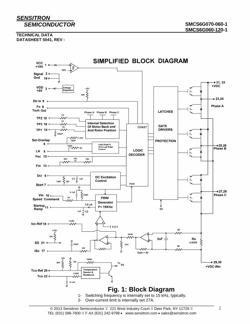
Fig. 1: Block Diagram 1- Switching frequency is internally set to 15 kHz, typically. 2- Over-current limit is internally set 27A.

SENSITRON
SEMICONDUCTOR
TECHNICAL DATA DATASHEET 5041, REV -
© 2013 Sensitron Semiconductor 221 West Industry Court Deer Park, NY 11729
TEL (631) 586-7600 F AX (631) 242-9798 www.sensitron.com [email protected]
SMCS6G070-060-1 SMCS6G060-120-1
3
ABSOLUTE MAXIMUM RATINGS (TC=25 oC) Characteristic Maximum
Operating DC Bus Supply Voltage SMCS6G070-060-1 SMCS6G060-120-1
400V 700V
Maximum Peak DC Bus Supply Voltage SMCS6G070-060-1 SMCS6G060-120-1
600V 800V
RMS Output Motor Current SMCS6G070-060-1 SMCS6G060-120-1
40 A 25A
Instantaneous Peak Output Current SMCS6G070-060-1 SMCS6G060-120-1
60 A 40A
Control Supply Voltage VCC 17 V
Logic Input Voltage -0.3 V to +5.5 V
Reference Source Current -30 mA
Speed Command Input Voltage - 0.3 V to +5.5 V
Operating and storage Junction Temperature -55 oC to +150
oC
IGBT Thermal Resistance RthjC Diode Thermal Resistance RthjC
0.45 oC/W
0.80 oC/W
Pin-to-Case Voltage Isolation, at room conditions 1500V DC
Lead Soldering Temperature, 10 seconds maximum, 0.125” from case * Tcase = 25° C
300°C
Recommended Operating Conditions (TC=25 oC)
Characteristic Maximum
Operating DC Bus Supply Voltage SMCS6G070-060-1 SMCS6G060-120-1
300V 600V
RMS Motor Current, TC=80 oC
SMCS6G070-060-1 SMCS6G060-120-1
40 A 20A
Control Supply Voltage VCC 15 V +/-10%

SENSITRON
SEMICONDUCTOR
TECHNICAL DATA DATASHEET 5041, REV -
© 2013 Sensitron Semiconductor 221 West Industry Court Deer Park, NY 11729
TEL (631) 586-7600 F AX (631) 242-9798 www.sensitron.com [email protected]
SMCS6G070-060-1 SMCS6G060-120-1
4
PARAMETER SYMBOL CONDITIONS (NOTE 1) MIN. TYP. MAX. UNITS
Power Output Section
DC Bus Leakage Current
SMCS6G070-060-1 at VCE=300V SMCS6G060-120-1 at VCE=600V
1.14 2.27
- mA
Collector-to-Emitter Saturation Voltage VCEsat, at VCC=15V
SMCS6G070-060-1 IC=30A IC=70A SMCS6G060-120-1 IC=40A
1.15 1.50 1.9
1.30 1.80 2.3
V
Diode Forward Voltage
SMCS6G070-060-1 IC=30A IC=70A . SMCS6G060-120-1 IC=40A
1.18 1.50 1.8
1.35 1.80 2.3
V
Control Section
Control Supply Current Icc at Vcc =15V Turn-On Threshold Vcc(+) Tc over operating range
8.0
10.0
40 11.5
mA V
5V Reference Section
Output Voltage Vref Output Current Io
4.7 -
5.0 -
5.3 30
V mA
Current-Sense Amplifier Section
Amplifier Voltage Gain Over-current detection voltage
16.3 0.45
18.3 0.50
20.3 0.55
mV/A V
Logic Input Section
Dir in, LA,Ov-Lap, Fm High-Level Input Voltage Threshold Dir in, LA, Ov-Lap, Fm Low-Level Input Voltage Threshold Fsc High-Level Input Voltage Threshold Fsc Low-Level Input Voltage Threshold Fsc Middle-Level Input Voltage Threshold
3.5 - 4 - 2
- - - - 2.5
- 1.5 - 1 3
V V V V V
Tachometer
Tachometer Output High Level Voh Tachometer Output Low Level Vol
4.5 -
- -
5.0 0.50
V V
PWM Section
PWM Frequency Fs 13 15 17 kHz
Over-Temperature Shutdown
Over-Temperature Shutdown 106 111 116 oC
Over-Temperature Shutdown Hysteresis 15 oC
SPECIFICATION NOTES:
1- All parameters specified for Ta = 2C, Vcc = 15Vdc, and all Phase Outputs unloaded. All negative currents shown are sourced by (flow from) the pin under test

SENSITRON
SEMICONDUCTOR
TECHNICAL DATA DATASHEET 5041, REV -
© 2013 Sensitron Semiconductor 221 West Industry Court Deer Park, NY 11729
TEL (631) 586-7600 F AX (631) 242-9798 www.sensitron.com [email protected]
SMCS6G070-060-1 SMCS6G060-120-1
5
Package Drawing Top View
(All dimensions are in inches, tolerance is +/- 0.010”)
Base Plate Flatness 0.010” Concave
SMC6GXXX-XXX-1
Fig. 2: Package Outline

SENSITRON
SEMICONDUCTOR
TECHNICAL DATA DATASHEET 5041, REV -
© 2013 Sensitron Semiconductor 221 West Industry Court Deer Park, NY 11729
TEL (631) 586-7600 F AX (631) 242-9798 www.sensitron.com [email protected]
SMCS6G070-060-1 SMCS6G060-120-1
6
Package Pin Locations
(All dimensions are in inches; tolerance is +/- 0.005” except otherwise specified)
Fig. 3: Package Outline

SENSITRON
SEMICONDUCTOR
TECHNICAL DATA DATASHEET 5041, REV -
© 2013 Sensitron Semiconductor 221 West Industry Court Deer Park, NY 11729
TEL (631) 586-7600 F AX (631) 242-9798 www.sensitron.com [email protected]
SMCS6G070-060-1 SMCS6G060-120-1
7
PIN OUT
PIN NUMBER
NAME DESCRIPTION
1 +15V Input
The +15V power supply connection for the controller. Under-voltage lockout keeps all outputs off for Vcc below 9 to 10.5V. The return of +15V is Pin 2. The input current requirement is 50mA without any external loads on Pin 3. Recommended input range is 13.5V min, 16.5V max. +15V supply is recommended to be an isolated power supply.
2, 19 Signal Gnd
Return for +15V supply, and +5V output Reference ground for all control signals of the device. All bypass capacitors and compensation components must be connected as close as possible to Pins 2 and 19. This ground is internally connected to the +VDC Rtn. It is preferred not to have external connection between Signal Gnd and +VDC Rtn at Pins 29 and 30.
3 VDD
(+5V Output)
+5V Output. . The maximum output current is 30mA. The return of +5V is Pin
2. This Pin should be bypassed to Gnd with 3-5F capacitor. The range of this output is 4.7V to 5.3V.
4 Ov-Lap
Overlap Commutation Angle Select Low: Overlap commutation High: 120° commutation This pin has a pull-up resistor of 100K.
5 LA
The lead angle control input. The lead angle settings are: LA (Low) Lead angle 7.5 degrees LA (High) Lead angle 15 degrees The pin has a pull-down resistor of 100K.
6 Dci DC excitation time setting pins When Vin ≥ 1 V (typ.), the START pin goes low to start DC excitation. The duration of the DC excitation mode is given by tdc Tdc = 0.69. R1. C1 sec R1 is set internally to 150 K ohms, and C1=1.0 uF
After the Dci pin reaches VDD/2, the controller moves from DC excitation to forced commutation mode.
7 Start
8 Tachometer
Output
Tachometer Output Variable frequency output proportional to the motor speed. The pulse duty cycle is 50%. There are 3 pulses every 360 electrical degrees. The number of pulses per motor revolutions is P*3/2. The Tachometer output frequency is
.
40
P nft Hz
Where P is the number of poles, n is the motor speed in rpm.
SENSITRON
SEMICONDUCTOR
TECHNICAL DATA DATASHEET 5041, REV -
© 2013 Sensitron Semiconductor 221 West Industry Court Deer Park, NY 11729
TEL (631) 586-7600 F AX (631) 242-9798 www.sensitron.com [email protected]
SMCS6G070-060-1 SMCS6G060-120-1
8
9 Dir-in
Rotation direction input High or open : Reverse rotation (A → C → B) Low : Forward rotation (A → B → C) The pin has a pull-up resistor of 10K. It is not safe to reverse the direction of rotation when the motor is running at high speed. Reduce the command input to a low speed, and then reverse direction. It is not safe to stop and restart while the motor is running at high speed. The motor will be forced to parking if restated while spinning, resulting in DC bus over-voltage due to regenerative action.
10 Vin
Speed Command Input (Duty Cycle Control Input) 0 ≤ Vin ≤ Vin (L): Output off Vin (L) ≤ Vin ≤ Vin (H): Set the PWM duty cycle according to the analog input. Vin (H) ≤ Vin ≤ VDD: Duty cycle = 100% (63/64) 0.8V < Vin (L) <1.2 V, 1.0V typical 3.8V < Vin (H) <4.2 V, 4.0V typical This pin has a pull-down resistor of 100K.
11 Startup-Ramp Enable/Disable
Startup Ramp (Soft Start). The ramp is initiated when this input is changed from low state to open state. Set a startup commutation time and duty cycle ramp-up. Connect this pin to a capacitor to set the ramp-up time. The capacitor charge current Isc is 2.6uA < Isc <5.0 uA, 3.8uA typical This pin is internally connected to C2 of 1.0 uF. The ramp-up time duration, is given by
Trise=Vin(V)*C2(uF)/3.8(uA) sec
where C2 is the total capacitance connected to Pin 11, in uF, and Vin is the speed command voltage applied at Pin 9 in volts. The ram-up time duration depends on the motor and its load. It should be optimized experimentally. This pin can be used as an Enable/Disable input using an open collector switch. If pulled down to zero, PWM duty cycle will go to zero and the motor will coast.
12 Fsc
Forced Commutation Frequency Select Input Low : Fsc = 2.5 Hz Middle : Fsc = 5 Hz High or open : Fsc = 10 Hz This pin has a pull-up resistor of 10K.
SENSITRON
SEMICONDUCTOR
TECHNICAL DATA DATASHEET 5041, REV -
© 2013 Sensitron Semiconductor 221 West Industry Court Deer Park, NY 11729
TEL (631) 586-7600 F AX (631) 242-9798 www.sensitron.com [email protected]
SMCS6G070-060-1 SMCS6G060-120-1
9
PIN OUT (continued)
13 Fm
This Pin together with Pin 12, set an upper limit of the maximum commutation frequency. Fsc = Low Fm = Low , Maximum commutation frequency Fm = 162 Fm = High or Open , Maximum commutation frequency Fm = 325 Fsc = High or Middle Fm =Low , Maximum commutation frequency Fm = 1302 Fm = High or Open , Maximum commutation frequency Fm = 2604 The pin has a pull-up resistor of 30K.
14 TP1 This is for factory testing Keep This pin floating.
15 TP2
Motor back EMF feedback information. This input is used to optimize back EMF sensing together with the TP3 input at Pin 16 Keep This pin floating.
16 TP3 Motor back EMF reference input Keep This pin floating.
17 Iso
Current Sense Amplifier Output for external monitoring. This pin is internally connected to the over-current comparator for cycle-by-cycle current limiting. It is recommended to have the over-current limit 20-30% higher than the target peak motor current. The gain of Iso is internally set to 0.0183 V/A.
18 Ioc-Ref -
Over-current Limit Adjustment. Connect a resistor Rg KOhms between Pins 18 and 19 to decrease the current amplifier gain and increase peak current limit. The current amplifier gain attenuation due to Rg will be
Kc = (5+Rg)/(80+6 Rg)
The output signal gain at Pin 17 will be 0.11*KC V/A. The internal over-current shutdown threshold is 0.5V The current limit 27A when Rg is open, and 46A when Rg is short
20 Tco-Ref Over-Temperature Shutdown Reference. It is internally set to 1.11V using a resistor divider of 50K pull-up to +5V, 12K pull-down, and 1000K feedback.
SENSITRON
SEMICONDUCTOR
TECHNICAL DATA DATASHEET 5041, REV -
© 2013 Sensitron Semiconductor 221 West Industry Court Deer Park, NY 11729
TEL (631) 586-7600 F AX (631) 242-9798 www.sensitron.com [email protected]
SMCS6G070-060-1 SMCS6G060-120-1
10
PIN OUT (continued)
21 SD
It is an active low, dual function input/output pin. It is internally
pulled high to +15V by 15K . As a low input it shuts down all
IGBTs regardless of the Hin and Lin signals.
SD is internally activated by the over-temperature shutdown, or
desaturation protection
SD can be used to shutdown all IGBTs by an external command. An
open collector switch shall be used to pull down SD externally.
SD can be used as a fault condition output. Low output at SD
indicates a latching fault situation.
SD is automatically cleared during more startup.
22 Tco
Analog output of case temperature sensor. The sensor output gain is
0.010 V/oC, with zero DC offset. This sensor can measure only positive
oC. The internal impedance of this output is 4.99K
The internal block diagram of the temperature sensor is shown in Fig.
12.
23, 24 Phase A Output Phase A terminals. Both terminals shall be used.
25, 26 Phase B Output Phase B terminals. Both terminals shall be used.
27, 28 Phase C Output Phase C terminals. Both terminals shall be used.
29, 30 +VDC Return Motor supply DC bus return. Both terminals shall be used.
31, 32 +VDC DC Bus Positive Input. Both terminals shall be used. +VDC bus should be bypassed to +VDC Rtn with adequately voltage-rated low ESR capacitor.
Case NC Not connected
SENSITRON
SEMICONDUCTOR
TECHNICAL DATA DATASHEET 5041, REV -
© 2013 Sensitron Semiconductor 221 West Industry Court Deer Park, NY 11729
TEL (631) 586-7600 F AX (631) 242-9798 www.sensitron.com [email protected]
SMCS6G070-060-1 SMCS6G060-120-1
11
Application Information
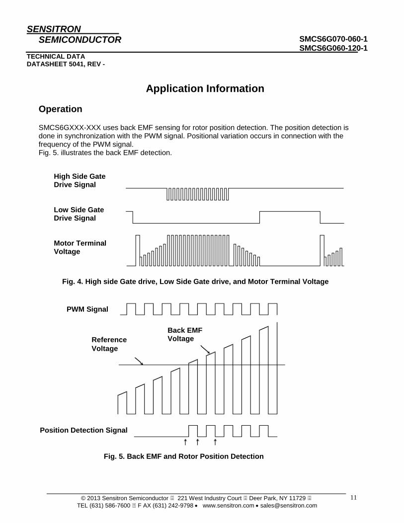
Operation SMCS6GXXX-XXX uses back EMF sensing for rotor position detection. The position detection is done in synchronization with the PWM signal. Positional variation occurs in connection with the frequency of the PWM signal. Fig. 5. illustrates the back EMF detection.
High Side Gate Drive Signal Low Side Gate Drive Signal Motor Terminal Voltage
Fig. 4. High side Gate drive, Low Side Gate drive, and Motor Terminal Voltage
Reference
Voltage
Back EMF Voltage
PWM Signal
Position Detection Signal
Fig. 5. Back EMF and Rotor Position Detection
SENSITRON
SEMICONDUCTOR
TECHNICAL DATA DATASHEET 5041, REV -
© 2013 Sensitron Semiconductor 221 West Industry Court Deer Park, NY 11729
TEL (631) 586-7600 F AX (631) 242-9798 www.sensitron.com [email protected]
SMCS6G070-060-1 SMCS6G060-120-1
12
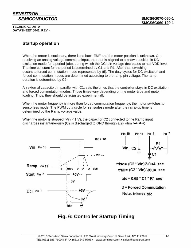
Startup operation
When the motor is stationary, there is no back-EMF and the motor position is unknown. On receiving an analog voltage command input, the rotor is aligned to a known position in DC excitation mode for a period (tdc), during which the DCI pin voltage decreases to half VDD level. The time constant for the period is determined by C1 and R1. After that, switching occurs to forced commutation mode represented by (tf). The duty cycles for DC excitation and forced commutation modes are determined according to the ramp pin voltage. The ramp duration is determined by C2. An external capacitor, in parallel with C1, sets the times that the controller stays in DC excitation and forced commutation modes. Those times vary depending on the motor type and motor loading. Thus, they should be adjusted experimentally.
When the motor frequency is more than forced commutation frequency, the motor switches to sensorless mode. The PWM duty cycle for sensorless mode after the ramp-up time is determined by the Ramp voltage value. When the motor is stopped (Vin < 1 V), the capacitor C2 connected to the Ramp input discharges instantaneously (C2 is discharged to GND through a 2k ohm
Fig. 6: Controller Startup Timing
SENSITRON
SEMICONDUCTOR
TECHNICAL DATA DATASHEET 5041, REV -
© 2013 Sensitron Semiconductor 221 West Industry Court Deer Park, NY 11729
TEL (631) 586-7600 F AX (631) 242-9798 www.sensitron.com [email protected]
SMCS6G070-060-1 SMCS6G060-120-1
13
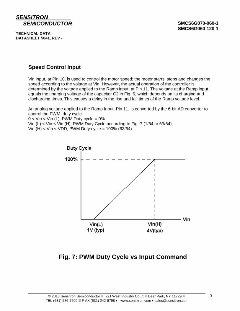
Speed Control Input Vin input, at Pin 10, is used to control the motor speed; the motor starts, stops and changes the speed according to the voltage at Vin. However, the actual operation of the controller is determined by the voltage applied to the Ramp input, at Pin 11. The voltage at the Ramp input equals the charging voltage of the capacitor C2 in Fig. 6, which depends on its charging and discharging times. This causes a delay in the rise and fall times of the Ramp voltage level. An analog voltage applied to the Ramp Input, Pin 11, is converted by the 6-bit AD converter to control the PWM duty cycle. 0 < Vin < Vin (L), PWM Duty cycle = 0% Vin (L) < Vin < Vin (H), PWM Duty Cycle according to Fig. 7 (1/64 to 63/64) Vin (H) < Vin < VDD, PWM Duty cycle = 100% (63/64)
Fig. 7: PWM Duty Cycle vs Input Command

SENSITRON
SEMICONDUCTOR
TECHNICAL DATA DATASHEET 5041, REV -
© 2013 Sensitron Semiconductor 221 West Industry Court Deer Park, NY 11729
TEL (631) 586-7600 F AX (631) 242-9798 www.sensitron.com [email protected]
SMCS6G070-060-1 SMCS6G060-120-1
14
Fault protection When a signal indicating the following faults is applied to the internal back EMF sensing, the output transistors are disabled. After time toff, about one second, the motor is restarted. This operation is repeated as long as a fault is detected. • The maximum commutation frequency is exceeded. • The rotation speed falls below the forced commutation frequency.
Fig. 8: Fault Detection & Re-Start

SENSITRON
SEMICONDUCTOR
TECHNICAL DATA DATASHEET 5041, REV -
© 2013 Sensitron Semiconductor 221 West Industry Court Deer Park, NY 11729
TEL (631) 586-7600 F AX (631) 242-9798 www.sensitron.com [email protected]
SMCS6G070-060-1 SMCS6G060-120-1
15
Two Quadrant Mode Of Operation Of BDC Motor Fig. 9 illustrates the four possible quadrants of operation for a BDC motor. Two-quadrant mode refers to a motor operating in quadrants I and III. With a two-quadrant BDC motor, friction is the only force to decelerate the load. Two-quadrant mode, modulates only the high-side devices of the output power stage, as shown in Fig. 4. The current paths within the output stage during the PWM on and off times are illustrated in Fig. 10. During the on time, both switches S1 and S4 are on, the current flows through both switches and the motor winding. During the PWM cycle off time, the upper switch S1 is shut off, and the motor current circulates through the lower switch S4 and D2. The motor is assumed to be operated in quadrants I or III. During direction reversal in quadrants II and IV, the motor current path is as shown in Fig. 11. Two-quadrant mode of operation is the most efficient mode, because the controller and motor switching losses are minimized. Also, EMI emission is minimum with two-quadrant mode of operation. The limitation of two-quadrant mode of operation is, it is not safe to reverse motor direction at high speed. In four-quadrant mode, both upper and lower switches are modulated. Motor current always decays during off time, eliminating any uncontrolled circulating current. In addition, the current always flows through the current sense resistor. For servo system applications, refer to SMCT6MXX-XX, or SMCT6GXX-XX motor controllers.
SENSITRON
SEMICONDUCTOR
TECHNICAL DATA DATASHEET 5041, REV -
© 2013 Sensitron Semiconductor 221 West Industry Court Deer Park, NY 11729
TEL (631) 586-7600 F AX (631) 242-9798 www.sensitron.com [email protected]
SMCS6G070-060-1 SMCS6G060-120-1
16
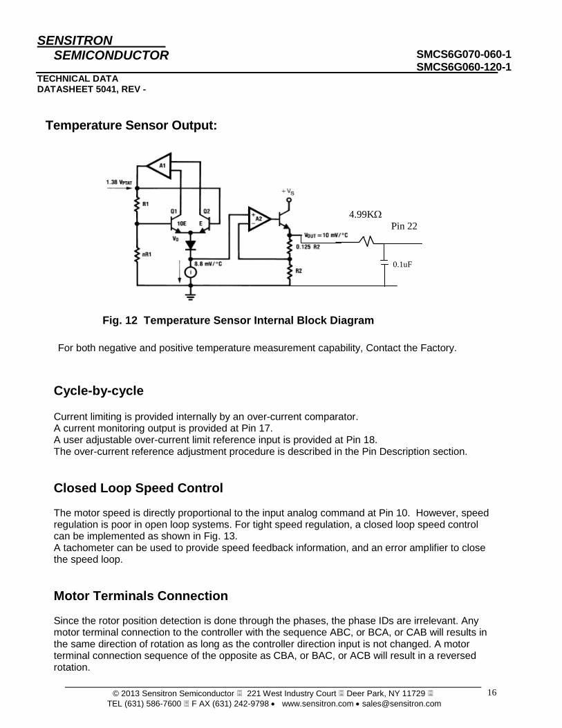
Temperature Sensor Output:
For both negative and positive temperature measurement capability, Contact the Factory.
Cycle-by-cycle Current limiting is provided internally by an over-current comparator. A current monitoring output is provided at Pin 17. A user adjustable over-current limit reference input is provided at Pin 18. The over-current reference adjustment procedure is described in the Pin Description section.
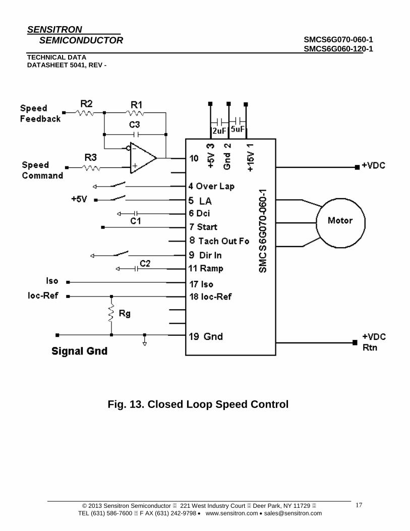
Closed Loop Speed Control The motor speed is directly proportional to the input analog command at Pin 10. However, speed regulation is poor in open loop systems. For tight speed regulation, a closed loop speed control can be implemented as shown in Fig. 13. A tachometer can be used to provide speed feedback information, and an error amplifier to close the speed loop.
Motor Terminals Connection Since the rotor position detection is done through the phases, the phase IDs are irrelevant. Any motor terminal connection to the controller with the sequence ABC, or BCA, or CAB will results in the same direction of rotation as long as the controller direction input is not changed. A motor terminal connection sequence of the opposite as CBA, or BAC, or ACB will result in a reversed rotation.
Fig. 12 Temperature Sensor Internal Block Diagram
0.1uF
Pin 22
4.99K
SENSITRON
SEMICONDUCTOR
TECHNICAL DATA DATASHEET 5041, REV -
© 2013 Sensitron Semiconductor 221 West Industry Court Deer Park, NY 11729
TEL (631) 586-7600 F AX (631) 242-9798 www.sensitron.com [email protected]
SMCS6G070-060-1 SMCS6G060-120-1
17
Fig. 13. Closed Loop Speed Control
SENSITRON
SEMICONDUCTOR
TECHNICAL DATA DATASHEET 5041, REV -
© 2013 Sensitron Semiconductor 221 West Industry Court Deer Park, NY 11729
TEL (631) 586-7600 F AX (631) 242-9798 www.sensitron.com [email protected]
SMCS6G070-060-1 SMCS6G060-120-1
18
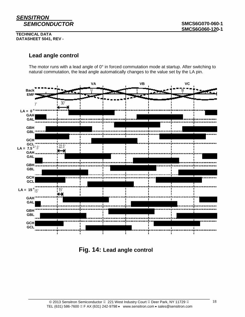
Lead angle control
The motor runs with a lead angle of 0° in forced commutation mode at startup. After switching to natural commutation, the lead angle automatically changes to the value set by the LA pin.
Fig. 14: Lead angle control
Back EMF
LA = 0 o
GAH GAL
GBH GBL
GCH GCL
LA = 7.5 o
GAH GAL
GBH GBL
GCH GCL
LA = 15
o
GAH GAL
GBH GBL
GCH GCL
VA
VB
VC

SENSITRON
SEMICONDUCTOR
TECHNICAL DATA DATASHEET 5041, REV -
© 2013 Sensitron Semiconductor 221 West Industry Court Deer Park, NY 11729
TEL (631) 586-7600 F AX (631) 242-9798 www.sensitron.com [email protected]
SMCS6G070-060-1 SMCS6G060-120-1
19
Overlap commutation
When Over-Lap (Pin 4) = high, the controller is configured to allow for 120° commutation. When Over-Lap (Pin 4)= low, it is configured to allow for overlap commutation. In overlap commutation, there is an overlap period during which both the outgoing transistor and incoming transistor are conducting (as shown in the shaded areas). This period varies according to the lead angle.
Fig. 15: Overlap commutation
Back EMF
LA = 7.5 o
GAH GAL
GBH GBL
GCH GCL
LA = 15
o
GAH GAL
GBH GBL
GCH GCL
VA
VB
VC

SENSITRON
SEMICONDUCTOR
TECHNICAL DATA DATASHEET 5041, REV -
© 2013 Sensitron Semiconductor 221 West Industry Court Deer Park, NY 11729
TEL (631) 586-7600 F AX (631) 242-9798 www.sensitron.com [email protected]
SMCS6G070-060-1 SMCS6G060-120-1
20
DC Bus Filtering To minimize the circuit parasitic inductance effect on the power stage, the layout of Fig. 14 is
suggested. C1, and C2 are 0.5F to 1F ceramic capacitors, connected across the DC bus as close as possible to the controller. Also, a bulk low ESR capacitor C3 with adequately voltage-rating shall be used.
Fig. 16: DC Bus Bypass Capacitors

SENSITRON
SEMICONDUCTOR
TECHNICAL DATA DATASHEET 5041, REV -
© 2013 Sensitron Semiconductor 221 West Industry Court Deer Park, NY 11729
TEL (631) 586-7600 F AX (631) 242-9798 www.sensitron.com [email protected]
SMCS6G070-060-1 SMCS6G060-120-1
21
IGBT and Diode Switching Characteristics and Waveforms (for SMCS6G070-060-1) 1- Test Conditions: VCE=280V, IC= 25A Test Results: Rise time tr= 66 nsec, Fall time tf= 52 nsec Current Scale is 20A/div, Voltage Scale is 50V/div, Power Loss Scale is 2000Watt/div Turn On Switching Loss = 0.47 mJ, Turn Off Switching Loss = 0.8 mJ
Fig. 17: IGBT Switching Performance

SENSITRON
SEMICONDUCTOR
TECHNICAL DATA DATASHEET 5041, REV -
© 2013 Sensitron Semiconductor 221 West Industry Court Deer Park, NY 11729
TEL (631) 586-7600 F AX (631) 242-9798 www.sensitron.com [email protected]
SMCS6G070-060-1 SMCS6G060-120-1
22
2- Test Conditions: VCE=280V, IC= 35A Test Results: Rise time tr= 102 nsec, Fall time tf= 45 nsec Current Scale = 20A/div, Voltage Scale = 50V/div, Power Loss Scale = 4000Watt/div Turn On Switching Loss = 0.7 mJ, Turn Off Switching Loss = 1.4 mJ
IC
VCE
PLoss
Fig. 18: IGBT Switching Performance
SENSITRON
SEMICONDUCTOR
TECHNICAL DATA DATASHEET 5041, REV -
© 2013 Sensitron Semiconductor 221 West Industry Court Deer Park, NY 11729
TEL (631) 586-7600 F AX (631) 242-9798 www.sensitron.com [email protected]
SMCS6G070-060-1 SMCS6G060-120-1
23
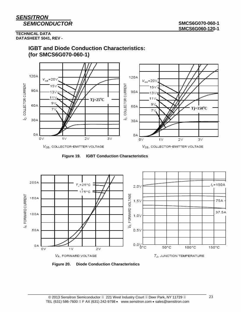
IGBT and Diode Conduction Characteristics: (for SMCS6G070-060-1)
Figure 20. Diode Conduction Characteristics
Figure 19. IGBT Conduction Characteristics
Tj=25oC
Tj=150oC

SENSITRON
SEMICONDUCTOR
TECHNICAL DATA DATASHEET 5041, REV -
© 2013 Sensitron Semiconductor 221 West Industry Court Deer Park, NY 11729
TEL (631) 586-7600 F AX (631) 242-9798 www.sensitron.com [email protected]
SMCS6G070-060-1 SMCS6G060-120-1
24
Cleaning Process: Suggested precaution following cleaning procedure: If the parts are to be cleaned in an aqueous based cleaning solution, it is recommended that the parts be baked immediately after cleaning. This is to remove any moisture that may have permeated into the device during the cleaning process. For aqueous based solutions, the recommended process is to bake for at least 2 hours at 125
oC.
Do not use solvents based cleaners.
Soldering Procedure: Recommended soldering procedure Signal pins 1 to 22: 210C for 10 seconds max Power pins 23 to 32: 260C for 10 seconds max. Pre-warm module to 125C to aid in power pins soldering.
DISCLAIMER: 1- The information given herein, including the specifications and dimensions, is subject to change without prior notice to improve product characteristics. Before ordering, purchasers are advised to contact the Sensitron Semiconductor sales department for the latest version of the datasheet(s). 2- In cases where extremely high reliability is required (such as use in nuclear power control, aerospace and aviation, traffic equipment, medical equipment , and safety equipment) , safety should be ensured by using semiconductor devices that feature assured safety or by means of users’ fail-safe precautions or other arrangement . 3- In no event shall Sensitron Semiconductor be liable for any damages that may result from an accident or any other cause during operation of the user’s units according to the datasheet(s). Sensitron Semiconductor assumes no responsibility for any intellectual property claims or any other problems that may result from applications of information, products or circuits described in the datasheets. 4- In no event shall Sensitron Semiconductor be liable for any failure in a semiconductor device or any secondary damage resulting from use at a value exceeding the absolute maximum rating. 5- No license is granted by the datasheet(s) under any patents or other rights of any third party or Sensitron Semiconductor. 6- The datasheet(s) may not be reproduced or duplicated, in any form, in whole or part, without the expressed written permission of Sensitron Semiconductor. 7- The products (technologies) described in the datasheet(s) are not to be provided to any party whose purpose in their application will hinder maintenance of international peace and safety nor are they to be applied to that purpose by their direct purchasers or any third party. When exporting these products (technologies), the necessary procedures are to be taken in accordance with related laws and regulations.