pn junction and zener diode 12 class project.ppt
22
in DEPARTMENT OF PHYICS MOTHER TERESA SR. SEC. CO-ED SCHOOL BHOPAL MOTHER TERESA SR. SEC. CO-ED SCHOOL KOLAR ROAD BHOAPL DEPARTMENT OF PHYSICS PROJECT REPORT INVESTIGATORY PROJECT ON PN JUNCTION AND DIODES PROJECT REPORT Submitted by Govind Patel Submitted to Mrs Ratna Hajela RegisterationNo:
-
Upload
shivam-soni -
Category
Education
-
view
6.582 -
download
618
Transcript of pn junction and zener diode 12 class project.ppt

in
DEPARTMENT OF PHYICS
MOTHER TERESA SR. SEC. CO-ED SCHOOL
BHOPAL
MOTHER TERESA SR. SEC. CO-ED SCHOOL
KOLAR ROAD BHOAPLDEPARTMENT OF PHYSICS
PROJECT REPORT
INVESTIGATORY PROJECT ON
PN JUNCTION AND
DIODES
PROJECT REPORT
Submitted by
Govind Patel
Submitted toMrs Ratna Hajela
RegisterationNo:

In the accomplishment of this project
successfully, many people have best
owned upon me their blessings and the
heart pledged support, this time I am
utilizing to thank all the people who
have been concerned with project.
Primarily I would thank god for being
able to complete this project with
success. Then I would like to thank my
principal Mr. James MJ and physics
teacher Mrs Ratna hajela, whose
valuable guidance has been the ones
that helped me patch this project and
make it full proof success her
suggestions and her instructions has
served as the major contributor towards
the completion of the project. Then I
would like to thank my parents and
friends who have helped me with their
valuable suggestions and guidance has
been helpful in various phases of the
completion of the project. Last but not
the least I would like to thank my
classmates who have helped me a lot.
ACKNOWLEDGEMENT

CERTIFICATE
This is to certify that project
work titled A STUDY ON PN
JUNCTIONS AND DIODES being
submitted by Govind Patel a
student of class XII-A has
successfully completed the research
on the below mentioned project
under the guidance of Mrs Ratna
Hajela ( Subject Teacher ) during
the year 2016-17 in partial
fulfillment of physics practical
examination conducted by AISSCE
Signature of external
examiner
Signature of
physics teacher

INDEX
• PN Junction
• Diode Equation
• Zener Diodes

Semiconductor: An Introduction
• Conductors: Allow Electric
current to flow through them
• Insulators: Do not Allow Electric current to flow through them
• Semiconductors: Materials whose conductivity lies in between of Conductors and Semiconductor

Insulators, Semiconductors,and Metals: Comparison
This separation of the valence and conduction bands determines the electrical properties of the material
Insulators have a large energy gap electrons can’t jump from valence to
conduction bands no current flows
Conductors (metals) have a very small (or nonexistent) energy gap electrons easily jump to conduction
bands due to thermal excitation current flows easily
Semiconductors have a moderate energy gap only a few electrons can jump to the
conduction bandleaving “holes”
only a little current can flow

P-N JUNCTION
Also known as a diode
One of the basics of semiconductor
technology -
Created by placing n-type and p-
type material in close contact
Diffusion - mobile charges (holes) in
p-type combine with mobile
charges (electrons) in n-type

P-N JUNCTION
Region of charges left behind
(dopants fixed in crystal lattice)
Group III in p-type (one less
proton than Si- negative charge)
Group IV in n-type (one more
proton than Si - positive charge)
Region is totally depleted of mobile
charges - “depletion region”
Electric field forms due to fixed
charges in the depletion region
Depletion region has high
resistance due to lack of mobile
charges

THE P-N JUNCTION
Direction of
Current

DEPLETION LAYER FORMATION
The “potential” or voltage across
the silicon changes in the
depletion region and goes from +
in the n region to – in the p region

Biasing the P-N Diode
Forward
Bias
Applies -
voltage to the
n region and
+ voltage to
the p region
CURRENT!
Reverse Bias
Applies +
voltage to n
region and –
voltage to p
region
NO
CURRENT
DIODES CAN BE
CONSIDERED AS
SWITCH

P-N Junction – Reverse Bias
positive voltage placed on n-type material
electrons in n-type move closer to positive terminal, holes in p-type move closer to negative terminal
width of depletion region increasesallowed current is essentially zero (small
“drift” current)
No current Flow
Depletion layer width
Increses
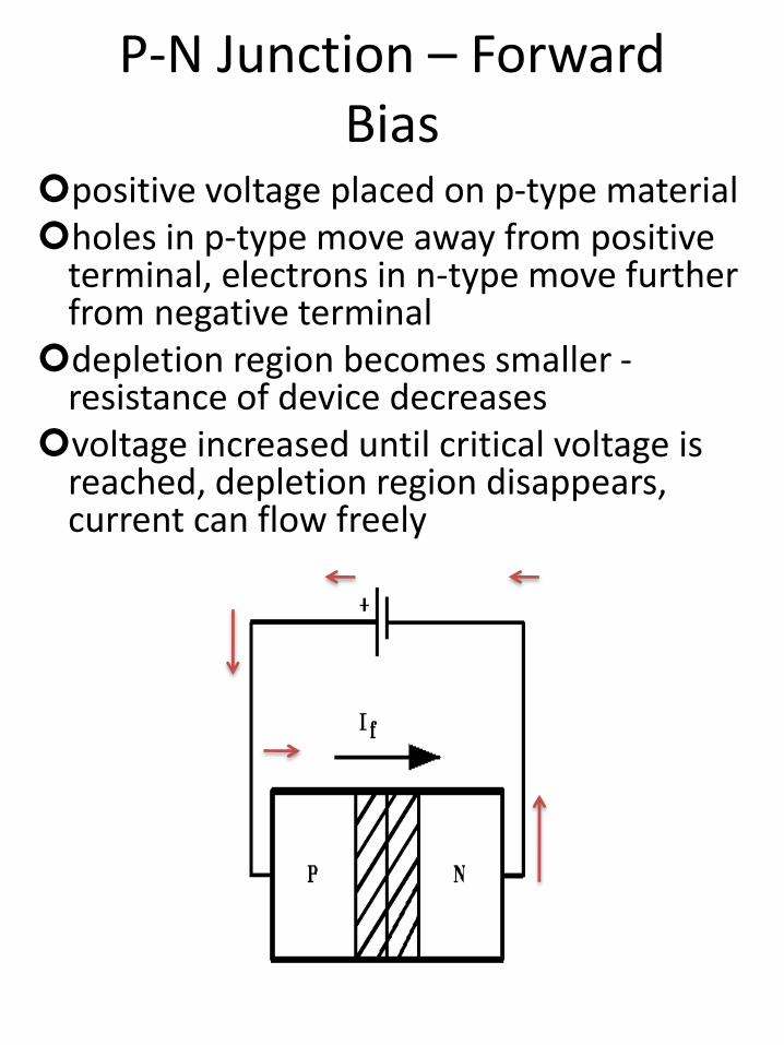
P-N Junction – Forward Bias
positive voltage placed on p-type materialholes in p-type move away from positive
terminal, electrons in n-type move further from negative terminal
depletion region becomes smaller -resistance of device decreases
voltage increased until critical voltage is reached, depletion region disappears, current can flow freely

P-N Junction - V-I characteristics
Voltage-Current relationship for a p-n junction (diode)

Current-Voltage Characteristics
THE IDEAL DIODE
Positive voltage yields
finite current
Negative voltage
yields zero currentREAL DIODE

Ideal diode equation
where:I = the net current flowing through the
diode;I0 = "dark saturation current", the diode
leakage current density in the absenceof light;V = applied voltage across the terminals
of the diode;q = absolute value of electron charge;k = Boltzmann's constant; andT = absolute temperature (K).
The diode equation gives an expression for the current through a diode as a function of voltage.
The Ideal Diode Law, expressed as:

Semiconductor diode -opened region
The p-side is the cathode, the n-side is the anode
The dropped voltage, VD is measured from the cathode to the anode
Opened: VD VF:
VD = VF
ID = circuit limited, in our model the VD
cannot exceed VF

Semiconductor diode -closed region
• Closed: VF < VD 0:
– VD is determined by the circuit, ID = 0 mA
• Typical values of VF: 0.5 ¸ 0.7 V
Cut-off: 0 < VD < VF:
ID 0 mA
Semiconductor diode - cut-off region

A Zener diode allows current to flow from its
anode to its cathode like a normal semiconductor
diode, but it also permits current to flow in the
reverse direction when its "Zener voltage" is
reached. Zener diodes have a highly doped p-n
junction. Normal diodes will also break down with
a reverse voltage but the voltage and sharpness of
the knee are not as well defined as for a Zener
diode. Also normal diodes are not designed to
operate in the breakdown region, but Zener
diodes can reliably operate in this region.
The device was named after Clarance Melvin
Zener, who discovered the Zener effect. Zener
reverse breakdown is due to electron quantum
tunnelling caused by a high strength electric
field. However, many diodes described as "Zener"
diodes rely instead on avalanche breakdown.
Both breakdown types are used in Zener diodes
with the Zener effect predominating under 5.6
V andavalanche breakdown above.
Zener diodes are widely used in electronic
equipment of all kinds and are one of the basic
building blocks of electronic circuits. They are
used to generate low power stabilized supply rails
from a higher voltage and to provide reference
voltages for circuits, especially stabilized power
supplies. They are also used to protect circuits
from over-voltage, especiallyelectrostatic
discharge
Zener diode

Zener diode shown with typical packages.Reverse current is
shown.
Zener diodes are widely used as voltage references and
as shunt regulators to regulate the voltage across small circuits. When
connected in parallel with a variable voltage source so that it is reverse
biased, a Zener diode conducts when the voltage reaches the diode's
reverse breakdown voltage. From that point on, the relatively low
impedance of the diode keeps the voltage across the diode at that
value.[8]
In this circuit, a typical voltage reference or regulator, an input voltage,
UIN, is regulated down to a stable output voltage UOUT. The breakdown
voltage of diode D is stable over a wide current range and holds
UOUT relatively constant even though the input voltage may fluctuate
over a fairly wide range. Because of the low impedance of the diode
when operated like this, resistor R is used to limit current through the
circuit.
In the case of this simple reference, the current flowing in the diode is
determined using Ohm's law and the known voltage drop across the
resistor R; The value of R must satisfy two conditions :
1.R must be small enough that the current through D keeps D in
reverse breakdown. The value of this current is given in the data sheet
for D. For example, the common BZX79C5V6[9] device, a 5.6 V 0.5 W
Zener diode, has a recommended reverse current of 5 mA. If
insufficient current exists through D, then UOUT is unregulated and less
than the nominal breakdown voltage (this differs to voltage-regulator
tubes where the output voltage will be higher than nominal and could
rise as high as UIN). When calculating R, allowance must be made for
any current through the external load, not shown in this diagram,
connected across UOUT.
2.R must be large enough that the current through D does not destroy
the device.
2.If the current through D is ID, its breakdown voltage VB and its
maximum power dissipation PMAX correlate as such: .
A load may be placed across the diode in this reference circuit,
and as long as the Zener stays in reverse breakdown, the diode
provides a stable voltage source to the load. Zener diodes in this
configuration are often used as stable references for more
advanced voltage regulator circuits.
Shunt regulators are simple, but the requirements that the ballast
resistor be small enough to avoid excessive voltage drop during
worst-case operation (low input voltage concurrent with high load
current) tends to leave a lot of current flowing in the diode much of
the time, making for a fairly wasteful regulator with high quiescent
power dissipation, only suitable for smaller loads.
These devices are also encountered, typically in series with a
base-emitter junction, in transistor stages where selective choice
of a device centered around the avalanche or Zener point can be
used to introduce compensating temperature co-efficient balancing
of the transistor p–n junction. An example of this kind of use would
be a DC error amplifier used in aregulated power supply circuit
feedback loop system.
Zener diodes are also used in surge protectors to limit transient
voltage spikes.
Another application of the Zener diode is the use of noise caused
by its avalan che breakdown in a random number generator.

NCERT textbook class 12 NCERT physics lab Manuel INTERNET www.yahoo.com www.scribd.com www.google.com