Semiconductors and Junction Diodes - New Age International
79
CHAPTER 1 Semiconductors and Junction Diodes 1.1 Introduction Semiconductors constitute a large class of substances which have resistivities lying between those of insula- tors and conductors. The resistivity of semiconductors varies within wide limits, i.e., 10 –4 to 10 4 Ω-m and is reduced to a very great extent with an increase in temperature (according to an exponential law) as shown in Fig. 1.1. In Mendeleev’s periodic table, semiconductors form the group of elements shown in Fig. 1.2. The most typical and extensively em- ployed semiconductors whose electrical properties have been well investigated, are Germanium (Ge), Silicon (Si) and Tellurium (Te). The study of their electrical properties reveals that (i) Semiconductors have negative temperature Coefficient of resistance, i.e., the resistance of semiconductors decreases with increase in temperature and vice versa as shown in Fig. 1.1. For example, Germanium is actually an insulator at low temperatures but it becomes good conductor at high temperature. (ii) The resistivity of semiconductors lies between that of a good insulator and of a metal conductor, i.e., lies within the range 10 –4 to l0 4 Ω-m. (iii) The electrical conductivity of a semiconductors is very much affected when a suitable metallic impu- rity, e.g., Arsenic, Gallium, etc. is added to it. This property of semiconductors is most important. Group ↓ → Period III IV V VI VII II B C III Si P S IV Ge As Se V Sn Sb Te I Fig. 1.2 Position of Semiconductor Elements in the Mendeleev Table. Fig. 1.1 The Temperature Dependence of the Resistance in Semiconductors. i Th dA li i
Transcript of Semiconductors and Junction Diodes - New Age International

CHAPTER 1
Semiconductors and
Junction Diodes
1.1 Introduction
Semiconductors constitute a large class of substances which have resistivities lying between those of insula-tors and conductors. The resistivity of semiconductors varies within wide limits, i.e., 10–4 to 104 Ω-m and isreduced to a very great extent with an increase in temperature (according to an exponential law) as shown inFig. 1.1.
In Mendeleev’s periodic table, semiconductors form the group ofelements shown in Fig. 1.2. The most typical and extensively em-ployed semiconductors whose electrical properties have been wellinvestigated, are Germanium (Ge), Silicon (Si) and Tellurium (Te).The study of their electrical properties reveals that
(i) Semiconductors have negative temperature Coefficient of
resistance, i.e., the resistance of semiconductors decreaseswith increase in temperature and vice versa as shown inFig. 1.1. For example, Germanium is actually an insulator atlow temperatures but it becomes good conductor at hightemperature.
(ii) The resistivity of semiconductors lies between that of a good insulator and of a metal conductor, i.e.,
lies within the range 10–4 to l04 Ω-m.
(iii) The electrical conductivity of a semiconductors is very much affected when a suitable metallic impu-rity, e.g., Arsenic, Gallium, etc. is added to it. This property of semiconductors is most important.
Group
↓ →Period
III IV V VI VII
II B C
III Si P S
IV Ge As Se
V Sn Sb Te I
Fig. 1.2 Position of Semiconductor Elements in the Mendeleev Table.
Fig. 1.1 The Temperature Dependence of theResistance in Semiconductors.
i Th d A li i

Today no society is considered modern or developed unless it has sizable electronics industry. We knowthat there can be no electronics industry without the semiconductors and related technologies. Obviously,semiconductors form the backbone of electronics. We find that semiconductors affect all walks of life whetherit is communications, computers, biomedical, power, aviation, defence, entertainment etc. The transistors, in-tegrated circuits (IC), lasers and detectors, sensors and other semiconductor devices through the items of dailyuse affecting our daily life.
In recent years a number of devices based on semiconductors have been developed that are of great practi-cal applications in electronics. Most important of these are semiconductor diodes, transistors and ICs. A tran-sistor, which is a three terminal device having properties similar to those of a vacuum tube (triode), butrequires no cathode power, and at the same time offers the hope of practically long life. In modern electronicsystems, the complete electronic circuit, containing many transistors, resistors, diodes, capacitors etc. is fabri-cated on a single chip is called an Integrated Circuit (IC). Recently, a new type of transistor which is calledmetal oxide semiconductor (MOS) transistor has become very useful in microelectronic circuits. This MOStransistor can be used also as a capacitor. In recent years, taking advantage of the silicon integrated circuittechnology, a new field has emerged which attempts to combine the sensor, aculator and the control circuit onas one integrated unit. In this sense it emulates a biological system. These are known as smart sensors,
microsystem technology (MST) or microelectromechanical systems (MEMS). It has been possible to fashionminiature mechanical devices such as gears, motors, springs etc. Their combination with sensing and actuat-ing functions has given researchers and engineers the tools to build microsystems that could not be imaginedearlier. This technology is doing the mechanical system what the invention of transistors and ICs did to theelectronic systems. MEMS devices are small in size, light weight, low cost, reliable, with large batch fabrica-tion technology. The MEMS technology involves a large number of materials. Silicon forms the backbone ofthis systems also due to its excellent mechanical properties as well as mature micro-fabcrication technologyincluding lithography, etching and bonding. As compared to electronic valves, semiconductor devices offerthe following advantages: (i) low weight and small size (ii) no power for the filament (iii) long service life(thousands of hours) (iv) mechanical ruggedness (v) low power losses and (vi) low supply voltages. At thesame time semiconductor devices suffer from a number of disadvantages: (i) marked spread in parametersbetween devices within the same type (ii) deterioration in performance with time (ageing); higher noise levelthan in electronic valves (iii) unsuitability of most transistors for use at frequencies over tens of megahertz;(iv) low input resistance as compared with vacuum triodes; (v) inability to handle large power (vi) deteriora-tion in performance after exposure to radioactive emissions.
Continuing efforts in research and development, however, are eliminating or minimizing many of thedemerits of semiconductor devices. There are semiconductor rectifiers for currents of thousands of amperes.Replacement of germanium with silicon makes crystal diodes and transistors suitable for operation at temper-atures upto 125°C. There are transistors for operation at hundreds of megahertz and more, and also microwavedevices such as gunn diode, tunnel diode, etc. The field of semiconductors is rapidly changing. This isexpected to continue in the next decade with some of the changes that can be foreseen now. We expect organic
semiconductors to play prominent role during this decade. Diamond as semiconductor will also be important.Optoelectronic devices will provide three-dimensional integration of circuits, and optical computing.
Semiconductor devices impose a very small drain on power sources and make it possible to miniaturize oreven micro-miniaturize components and whole circuits. The minimum power for an electronic valve is 0.1watt, while for a transistor it may be one microwatt, or one hundred thousandth of the former.
Of course, semiconductor devices will not replace electronic valves in each and all applications, for thevalves are also being continually improved. Simply, crystal diodes and transistors may be advantageous insome uses and electronic valves in others.
Rapid progress in the fabrication of semiconductor structures has resulted into the reduction of threedimensional bulk systems to two-dimensional, one dimensional and finally to zero-dimensional systems.
2 Electronics—Theory and Applications

These reduced dimensional systems are used in future applications like improved semiconductor lasers andmicroelectronics.
Quantum Dots (QDs) represent ultimate reduction in the dimensionality of semiconductor devices. These are3-dimensional semiconductor structures only nanometers in size confining electrons and holes. QDs operateat the level of a single electron which is certainly the ultimate limit for an electronic device and are used as gainmaterial in lasers. QDs are used in quantum dot lasers, QD memory devices, QD photo-detectors and evenquantum cryptography. The emission wavelength of a quantum dot is a function of its size. Obviously, bymaking quantum dots of different sizes, we can create light of different colours (Eisler et al., Appl. Phys. Lett.;June 2002).
The semiconductor technology is based on the number of charges and their energy. The electronic devicessuch as transistors work due to flow of charge. The electron can be assumed as tiny rotating bar magnet withtwo possible orientations: spin-up or spin-down. An applied magnetic field can flip electrons from one state toanother. In this way, spin can be measured and manipulated to represent the 0’s 1’s of digital programming,analogous to the “current on and current off” states in a conventional silicon chip. The study of electron spin inmaterials is called spintronics. Spintronics is based on the direction of spin and spin coupling (Nature, April2002).
A revolutionary new class of semiconductor electronics based on the spin degree of freedom could becreated. The performance of conventional devices is limited in speed and dissipation whereas spintronicsdevices are capable of much higher speed at very low power. Spintronics transistors may work at a fasterspeed, are also smaller in size and will consume less power.
Electon spins can be oriented in one direction or the other, called spin-up or spin-down. When electronsspins are aligned in one direction, these create a net magnetic moment as observed in magnetic materials like,iron and cobalt. Magnetism is an intrinsic physical property associated with the spins of electrons in a material.The electron spin may exist not only in the up or down state but also in infinitely many intermediate states
because of its quantum nature depending on the energy of the system. This property may lead to highly parallelcomputation which could make a quantum computer work much faster for certain types of calculations. Inquantum mechanics, an electron can be in both spin-up and spin-down states, at the same time. The mixedstate could form the base of a computer, built around not binary bits but the quantum bits or qubit. It is anycombination of a 1 or a 0. The simplest device using spin-dependent effect is a sandwich with two magneticlayers surrounding a non-magnetic metal or insulator. If the two magnetic layers are different, then the magne-tization direction of one can be rotated with respect to the other. This leads to the utilization of these structuresas sensor elements and for memory elements. Scientists and engineers are now trying to use the property of theelectron-like spin rather than charge to develop new generation of microelectronic devices which may be moreversatile and robust than silicon chips and circuit elements. Spins appears to be remarkably robust and moveeasily between semiconductors. In case of electron transport from one material to another, the spins do not loseits orientation or scatter from impurities or structural effects.
All spintronics devices work accordingly to simple principle: information is stored into the spins as aparticular spin orientation (up or down); the spins being attached to mobile electrons, carry the informationalong the wire and the information is read at the terminal. Two recent discoveries:
(i) Optically induced long-lived coherent spin-state in semiconductors, and
(ii) Ferromagnetism in semiconducting GaMnAs will lead to revolutionary advances in photonics andelectronics, such as, very fast, very dense memory and logic at extremely low power, spin quantumdevices like Spin-Fets, Spin-LEDs, and Spin-RTDs and quantum computing in conventional semicon-ductors at room temperature. The emerging technology of spintronics may soon make it possible tostore movies on a palmpilot or build a new computer.
Semiconductors and Junction Diodes 3
To understand the operation of semiconductor devices, it is necessary to study the semiconductor materialsin some detail.
1.2 Atomic Structure and Energy Level
To understand how semiconductors work, one must have a good knowledge of atomic structure. We know thatmatter is composed of compounds and elements. The elements are the basic materials found in nature. Whenelements are combined to form a new material, we have a compound. The smallest particle that an element canbe reduced to and still retain its properties is called an atom.
Although the atoms of different elements have different properties, they all contain the same subatomicparticles. There are a number of different subatomic particles, but only three of these are of interest in basicelectronics—the proton, the neutron and the electron.
The proton and the neutrons are contained in the nucleus of the atom, and the electrons revolve around thenucleus along specific orbits. The electrons and the protons are the particles that have the electrical properties.Neutrons have no electrical charge. Usually, atoms have the same number of electrons and protons, and sothey are electrically neutral. If an atom does have more electrons, it is called a negative ion. If it has more pro-tons, it is called a positive ion.
Fig. 1.3 shows the representations of the atomic structures of H, B, Si, P and Ge atoms. Fig. 1.3 (a) repre-sents the hydrogen atom. It contains one electron revolving around one proton which is the nucleus. The nu-cleus of H atom contains no neutrons.
Fig. 1.3 (b) represents the structure of a Boron atom. Its nucleus contains 5 protons (P) and 5 neutrons (N).There are 5 electrons revolving around the nucleus in different orbit. There are two electrons in the first orbit, 2electrons in the second orbit and only 1 electron in the outermost or valence orbit.
Fig. 1.3 (c) represents the structure of a Silicon atom. It contains 14 protons and 14 neutrons in the nucleus.There are 14 electrons revolving around the nucleus in different orbits. There are 2 electrons in the first orbit, 8electrons in the second orbit and 4 electrons in the valence orbit.
Figs. 1.3 (d) and 1.3 (e) represent the structure of Phosphorus and Germanium atoms respectively. We notethat Phosphorus contains 5 electrons in the outermost orbit called valence electrons whereas Ge atom contains4 electrons in the outermost orbit.
The electrons in the inner orbits of an atom do not normally leave the atom. But the electrons which are inthe outermost orbit, so called valence orbit do not always remain confined to the same atom. Some of these va-lence electrons in certain materials called metals move in a random manner and may travel from one atom toanother in a crystal lattice. These electrons are called as free electrons. It is due to the presence of these freeelectrons in a material, conduction is possible and it constitutes the current. The electrons in the inner orbits ofthe atom remain bound to the nucleus and are, therefore, called bound electrons.
The tendency of an atom to give up its valence electrons depends on chemical stability. When an atom isstable, it resists giving up electrons, and when it is unstable, it tends to give up electrons. The level of stabilityis determined by the number of valence electrons, because the atom strives to have its outermost or valenceshell completely filled.
If an atom’s valence orbit is more than half filled, then atom tends to fill its orbit. So, since 8 is the maxi-mum electrons that can be held in the valence orbit, elements with 5 or more valence electrons make good in-
sulators, since they tend to accept rather than give up electrons. On the other hand, atoms with less than 4valence electrons tend to give up their electrons, thereby the valence shell is empty, this would allow the nextshell, which is already filled, to be the outermost shell. These atoms make the best electrical conductors. The,elements Si(14) and Ge(32) have 4 valence electrons, and are neither good conductors and nor good insulators.These are called semiconductors.
4 Electronics—Theory and Applications

Most characteristics of semiconductors can be easily explained by means of an energy level diagram. Weare familiar that each isolated atom has only a certain number of orbits available. These available orbits repre-sent energy levels for the electrons in the atom. According to Bohr’s theory of atomic structure only discrete
values of electron energies are possible. An electron energy is usually expressed in electron volt (l eV = 1.6 ×10⁻¹⁹ J = 1.6 × 10⁻¹² erg). An electron can have only certain permissible values, i.e., no electron can exist at anenergy level other than a permissible one’. Energy level diagram for hydrogen atom is shown in Fig. 1.4. Thepermissible energy levels for hydrogen atom are numbered n = 1, 2, 3 ... in increasing order of energy.
In any atom, an electron orbiting very close to the nucleus in the first orbit is tightly bound to the nucleusand possesses only a small amount of energy. The greater the distance of an electron from the nucleus, thegreater is its total energy. The total energy of an electron includes Kinetic and Potential energies. Obviously,an electron orbiting far from the nucleus would have a greater energy, and hence it can be easily knocked outof its orbit. This makes it clear that why the valence electrons having maximum energy take part in chemicalreactions and in bonding the atoms together to form solids.
When radiations impinge on an atom, the energy of the electrons increases. As a result, electrons are ex-cited to higher energy levels. The excited state does not last long and very soon, the electron after emitting outenergy in the form of heat, light or other radiations, fall back to the original energy level.
Semiconductors and Junction Diodes 5
Fig. 1.3 Atomic Structure of a Few Atoms.

1.3 Energy Band Diagrams in Solids
The simple energy level diagram of Fig. 1.4 for electron energies is no longer applicable when one discusses asolid. A solid is formed when atoms bond together. In a solid, the orbit of an electron is influenced not only by thecharges in its own atom but by electrons and nuclei of every atom in the solid. Each electron in a solid occupies adifferent position inside the solid and hence no two electrons can have exactly the same pattern of surroundingcharges. Obviously, the orbits of electrons in a solid are different.
When one is considering a solid in bulk, then the simple energy level diagram in Fig. 1.4 modifies to thatshown in Fig. 1.5. All electrons belonging to the first orbits have slightly different energy levels because notwo electrons see exactly the same charge envi-ronment. Since there are billions of first-orbitelectrons, the slightly different energy levelsform a group or band. Similarly, the billions ofsecond orbit electrons, all with slightly differentenergy levels, form the second energy band. Andall third orbit electrons form the third band.
Silicon is a commonly used semiconductorhaving atomic number 14. Obviously, it has 4electrons in its outermost or valence orbit.Clearly, the third band becomes the valence band(Fig. 1.5). In Fig. 1.5, all these three bands areshown completely filled. Although the thirdshell of an isolated atom of silicon is not com-pletely filled as it has only 4 electrons whereas itcould accommodate a maximum of 8 electrons,the third energy band or valence band of a bulksilicon material behaves as if completely filled.It is so, because in solid silicon each atom
6 Electronics—Theory and Applications
Fig. 1.4 Energy Levels of an Isolated Hydrogen Atom.
Fig. 1.5 Energy Bands of Silicon at Absolute Zero.

positions itself between four other silicon atoms, and each of these neighbours share an electron with the cen-tral atom. In this manner, each atom now has 8 electrons associated with it thereby filling the valence bandcompletely, i.e., all the permissible energy levels in the band are occupied by electrons. Obviously, no electronin a filled band can move and hence an electron in a completely filled band cannot contribute to electric cur-rent. At absolute zero temperature, electrons cannot move through the solid Silicon material and hence it actslike a perfect insulator. Beyond the valence band there is a conduction band. At absolute zero temperature, theconduction band is empty, i.e., no electron has enough energy to go into a conduction band. Definite amount ofenergy is needed to shift the electron from the valence band to the conduction band. This amount differs fromone substance to another substance and helps to classify them as conductors, insulators and semiconductors.
1.4 Conductors, Semiconductors and Insulators
The band structure in a solid determines whether the solid is an insulator or a conductor or a semiconductor.The bands are filled upto a certain level by the electrons within each atom. The highest band in which electronsare still predominantly attached to their atoms are found is called the valence band. This is the band in whichthe valence (outermost) electrons from each atom will be located. These are the electrons that are the possiblecarriers of electricity. However, in order for an electron to conduct, it must get up to a slightly higher energy sothat it is free of the grip of its atom.
Insulators. Let us consider the case when the valence band in full, i.e., when there are no more availableenergy levels. Then, a valence electron must jump (increase its energy) into the next higher band to be free. Ifthe energy gap between the valence band and the conduction band is too large, then the electron will not beable to make that jump. Such a material will not be a good conductor of electricity, and is called an insulator.
Forbidden energy gap in an insulator is about 5 eV or even more (Fig. 1.6 (a)). The band theory of solids tellsus that an insulator is a material in which the valence bands are filled and the forbidden energy gap betweenvalence band and conduction band is too great for the valence electrons cannot jump at normal temperaturesfrom VB to the CB. An insulator does not conduct at room temperature because there are no conductionelectrons in it. However, an insulator may conduct if its temperature is very high or if a high voltage is appliedacross it. This is known as the breakdown of the insulator.
Conductors. There are actually two possibilities for a substance to be a conductor. One is that the valence bandis not completely filled. Then an electron in the valence band can get free of its atom by simply jumping to a
Semiconductors and Junction Diodes 7
(a) (b) (c) (d)
Eg 5 eV or more≈ Eg 1 eV≈
ValenceBand
ValenceBand
ValenceBand
ValenceBand
ConductionBand
ConductionBand
ConductionBand
ConductionBand
Ene
rgy
(eV
)
Fig. 1.6 Energy Band Diagram for (a) Insulators, (b) and (c) Conductors, and (d) Semiconductors.

higher energy level within the same band. This jump requires a small amount of energy, and many electronscan, therefore, make that jump (Fig. 1.6 (b)).
Another situation in which a conductor results stems from the fact that the size of the energy gaps betweenthe valence band and the conduction band are very small and different for different materials. It can even dis-appear, when the valence band and conduction band overlap (Fig. 1.6(c)). Therefore, the band theory tells usthat we have a conductor when
(i) The valence band is not filled, so electrons can move to higher states in the valence band and be free,or
(ii) When there is no energy gap between the valence band and the conduction band, so electrons can eas-ily make the transitions from the valence to the conduction band e.g., metals.
Semiconductors. There is a case in between ‘conductor’ and ‘insulator’. A material with intermediateproperties is called a semiconductor. In a semiconductor,
(i) The valence band is filled, and(ii) Although there is an energy gap between the valence band and the conduction band yet the energy gap
is not very large.
The energy-band diagram for a semiconductor is shown in Fig. 1.6 (d). In this case, the forbidden energygap is of the order of 1 eV (for Silicon, Eg= 1.12 eV and for Ge, Eg = 0.72 eV). Silicon and Germanium arevery good examples of semiconductors. The gaps between their valence and conduction bands are sufficientlysmall that the normal thermal energy of the solid at room temperature is enough to knock a few electrons intothe conduction band. These electrons conduct a current, but, as the name ‘Semiconductor’ implies, a semicon-ductor does not conduct as best as a real conductor. We will discuss it later on. The conductivity of these sub-stances has a number of peculiarities:
(i) The dependence of conductivity on temperature is opposite to that of metals. The conductivity ofsemiconductors, in contradiction to that of conductors (metals), may decrease rapidly with temperature.At low temperatures, a semiconductor may become an insulator. Hence, the distinction betweensemiconductors and insulators is purely quantitative and, to a large extent, conventional. The resistanceof most semiconductors is considerably more sensitive to changes in temperature than metals. Compacttemperature meters of high sensitivity may be constructed using semiconducting thermal resistors(thermistors).
(ii) In a number of cases semiconductors may possess positive as well as negative temperature coefficient.
1.5 Fermi Level
In the preceding article, we have seen that as far as solid-state theory is concerned only the upper energy bands(valence bands) are of interest, since electrons at lower levels practically do not take part in interactions amongatoms. How can the behaviour of upper band electrons be described? Since we are dealing with a very largenumber of electrons, it is natural to use statistical physics methods and consider an aggregate of such electronsas a kind of gas, usually called as electron gas.
The state of each electron of such a gas may be represented by a point (px, py, pz) in momentum space. Thedirection of motion of an electron is parallel to its radius vector P and the energy of an electron depends on itsmomentum. Let us consider as a crude approximation that the electrons in solid behave like free particles, i.e.,we neglect the potential energy of the field in which the electrons move and the interaction between electrons.
If the electrons are free, the relationship between their energy and momentum is given by E = (1/2m)p2.
This means that in momentum space a surface of total energy is a sphere. Such a sphere is usually called a
8 Electronics—Theory and Applications

Fermi sphere. One may call the Fermi surface a surface of maximum energy as the states of an electron gas arecontained in a sphere of radius
p mEmax max= 2
It is most important to determine how the electrons may distribute themselves in a band among the energiesfrom zero upto Emax. The number of electrons per unit volume then can be accommodated up to an energy E isgiven by
nm
hE
e= 16 2
3
3 1 2
3
3 2π( ) // (1.1)
If the metal is in its ground state, which occurs at absolute zero, all electrons occupy the lowest possibleenergy levels compatible with the Pauli exclusion principle (i.e., each level can accomodate two electrons: onewith spin up and one with spin down), as indicated in Fig. 1.7(b). If the total number of electrons per unit vol-ume n0 is less than the total number of energy levels available in the band, the electrons will then occupy allenergy states up to a maximum energy, designated by EF, and called the Fermi energy. Thus the Fermi energy
EF is defined as the energy of the topmost filled level in the ground state of n electrons. If we set E = EF inEq. (1.1), we must have n = n0. Therefore for the Fermi energy we obtain the value
Eh
m
nF
e
=
20
2
3
8
3
π1.1(a)
The energy distribution of electrons in the metal ground state corresponds to the shaded area in Fig. 1.7(a).When the Fermi energy is equal to the energy band width, the band is fully occupied.
Semiconductors and Junction Diodes 9
Fig. 1.7 (a) Density of energy states of free electrons in a solid (b) and (c). Distribution of free electrons among energy states in theconduction band. (d) Occupation of energy states at a temperature different from absolute zero.

When band is not completely full, a small amount of energy is enough to excite the uppermost electrons tonearby energy levels as indicated in Fig. 1.7(c). However, only the uppermost electrons can be thermally about0.025 eV, which is very small compared with EF , and the exclusion principle makes it impossible for thelow-energy electrons to be excited into nearby occupied states. The distribution of electrons among the energylevel in a thermally excited state of the lattice corresponds to the shaded area in Fig. 1.7(d). The electronswhich have been thermally excited are those with an energy greater than EF. The states occupied by the excitedelectrons fall in an energy region of the order of 20 kT about EF.
From the above discussion one can easily conclude that the concept of Fermi level serves the reference en-ergy level from which all other energies are conveniently measured. The probability F(E) of a state corre-sponding to energy E being occupied by an electron at temperature T°K is given by
F EE E
kT
F
( )
exp
=+ −
1
1
1.1(b)
Here k is Boltzmann constant. Three cases of interest are:
(i) At T = 0°K, if E > EF then F(E) = 0, i.e., energy state is empty.
(ii) At T = 0°K, if E < EF then F(E) = 1, i.e., energy state is occupied by an electron,
(iii) At T ≠ 0°K, and E = EF then F(E) = 1/2, i.e., energy state is 50% occupied.
Obviously, one finds that at T = 0°K, all the energy states above EF are empty, whereas all those belowFermi energy (EF) are filled with electrons. With the rise in temperature, states above Fermi energy level (EF)no more remain empty. They are then occupied by the electrons to some extent. Fig. 1.8 shows the position ofFermi level in energy band diagram in the case of pure or intrinsic semiconductors. It depicts that Fermi levelfor an intrinsic semiconductor is situated in the middle of forbidden gap, [See eq. (1.9a)] i.e., between conduc-tion and valence band, and the position of Fermi level is independent of temperature. This reveals that whenthe temperature is raised there is a greater possibility of electrons being found above the Fermi level with anequal possibility of finding an electron vacancy so called ‘hole’ below Fermi level. We will discuss it in latersections.
1.6 Intrinsic Semiconductors
Semiconductor devices, e.g., diodes and transistors, are made from a single crystal for semiconductor material,e.g. germanium or silicon. To make a semiconductor device, a sample of semiconductor must be in its purest
10 Electronics—Theory and Applications
Fig. 1.8 Fermi Level in Intrinsic Semiconductor at 0°K.

form. A semiconductor in its purest form is called an intrinsic semiconductor. A semiconductor is not trulyintrinsic unless its impurity content is less than 1 part impurity in 100 million parts of semiconductor. As statedearlier that at 0°K temperature, the Fermi level (EF) in intrinsic semiconductors, lies nearly mid way between thevalence and conduction band.
As the temperature is raised, some electrons near the top of the valence band are thermally ionised intothe lowest levels of the conduction band. The conduction band now contains a few electrons, and thevalence band has a few missing electrons or holes*. Thermal ionization, therefore, is said to createhole-electron pairs, since there is one hole for each electron. As both electrons and holes transport chargethrough the semi-conductor, they are collectively termed charged carriers or simply carriers. In appliedelectric and magnetic fields a hole acts as if it is a positive electron. To understand the phenomenon ofconduction of current in a semiconductor, it is essential to study its crystal structure.
1.6 (a) Crystal Structure of Semiconductors
It is the nature of some solid materials to form themselves into bodies called crystals which have characteristicgeometric shapes. These are the crystalline substances. Exact opposites are those other solids which form intoshapeless masses and are said to be plastic, non crystalline, or amorphous. Quartz is a familiar example of crys-talline substances where as a block of rubber is amorphous. Elements and compounds both can be crystalline. Socan metals and non metals. Virtually all minerals are crystalline.
Externally, a crystal has several flat faces which are arranged symmetrically w.r.t. each other. Internally, ithas a certain orderly arrangement of atoms in a repeating system called a lattice. Both externally and internally, asingle crystal of a given true crystalline material looks like all other crystals of that material. A single crystal maybe large to the point of hugeness or it may be so small as to be visible only with the aid of magnifier.
Inside the crystal lattice, certain loosely bound electrons (called valence electrons) in the outer orbit of oneatom align themselves with similar electrons in adjacent atoms to form covalent bonds which hold the atomstogether in the orderly structure of the lattice. Thus, in any covalent bond there are shared electrons, so calledbecause they are shared by neighbouring atoms.
Germanium (Ge) and Silicon (Si) are two very typical semiconductors. In Germanium the atom has 32 elec-trons distributed in four orbits whereas in silicon there are 14 electrons distributed in three orbits. The outermostorbit called the valence orbit contain 4 electrons in each case (Fig. 1.3).
The crystals are tetrahedral in structure and each atom shares one of its electrons with its neighbour. Such asharing of its electrons between two neighbouring atoms is called a covalent bond. A simplified representationof the crystalline structure of a semiconductor (Ge) at absolute zero is shown in Fig. 1.9.
At very low temperature near absolute zero all the electrons in the atoms are tied up strongly by thesebonds, but with the rise of temperature, a few electrons break away from some of the covalent bonds and getthemselves freed creating vacant spaces, deficient of electrons known as holes. A hole is equivalent to a netpositive charge equal to that of electron. Whenever a free electron is generated, a hole is created simultaneously,i.e., free electrons and holes are always generated in pairs. Obviously, the concentration of free electrons andholes will always be equal in an intrinsic semiconductor. This type of generation of free-electron hole pairs insemiconductors is called as thermal generation.
Owing to the thermal vibrations the free electrons in a semiconductor crystal jump from one bound positionto another. This is equivalent to the motion of a hole relatively in opposite direction and thus gives an electriccurrent in the direction of motion of the hole. The conductivity of semiconductor is, therefore, due to the
Semiconductors and Junction Diodes 11
* When an electron moves from the valence band it leaves behind a vacant energy state with a positive charge. Moreover, as the electronmoving from the valence band is located at the top edge of the band has a negative effective mass and its absence in the valence band isassociated with a positive mass. The vacant energy state in the valence band therefore has a positive charge and a positive mass. Thevacant energy state is called a ‘hole’.

motion of the holes and of the electrons. [Fig. 1.10(b)]. Such intrinsic semiconductors produce very weak elec-tric current not adequate for useful work.
1.6 (b) Carrier (or Electron and Hole) Concentrations in Intrinsic Semiconductors
In order to calculate the intrinsic carrier concentration, we first calculate the number of electrons excited intothe conduction band at any temperature T°K and which in turn are free to migrate in the crystal. In carrying outthese calculations it will be assumed that the electrons in the conduction band behave as if they are free witheffective mass me
* and energy will be measured from the top of the valence band. We further take the electrondensity of states in the conduction band is equal to that for free electrons i.e.,
12 Electronics—Theory and Applications
Fig. 1.9 A Simplified Representation of the Crystalline Structure of a Semiconductor (Ge) at Absolute zero.
Fig. 1.10 (a) Crystalline Structure of Ge at room temperature; (b) Generation of Electron-hole Pair in anIntrinsic Semiconductor (Ge).
N Em
hE E
eg( )
( )( )
*/=
−1
2
22 2
1
21 2
π(1.2)
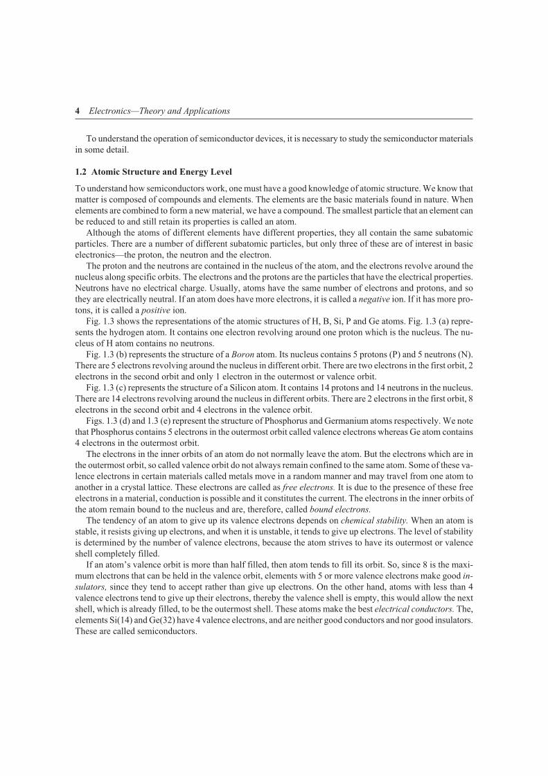
In addition to the density of states function we also require the probability function for calculating the electrondensity in the conduction band. The appropriate probability function is the Fermi function f (E) given by equa-tion (1.1). As stated earlier that Fermi level Ep is in the middle of the band gap in the case of intrinsic semicon-ductors. If (E – EF) < 4 kT, i.e., the lower edge of the conduction band is about 4kBT above EF, one can neglect1 in the denominator of equation (1.1) and Fermi function f(E) reduces to
F(E) = exp (EF – E)/kT (1.3)
The number of electrons per unit volume having their energy in the range dE in the conduction band can beobtained from
ne(E) dE = Ne(E) f(E) dE (1.4)
or n n E dEe eFg
=∞
∫ ( ) .
This leads to ne = Ne exp [(EF – Eg)/kT] (1.5)
Here Nm kT
he
e=
2
22
3
2π *
is called as the effective density of states in the conduction band. Equation (1.5) gives us the electron concen-tration in the conduction band.
In order to calculate the hole density nh where h refers to hole, we assume that the holes near the top of thevalence band behave as if they are free particles with an effective mass mh
* . One can express the density of hole
states in the valence band as
N E dEm
hE dEh
h( ) ( )*
/=
−1
2
22 2
3
21 2
πper unit volume
Here, one must remember that the energy is measured positive upwards from the top of the valence band. Iffh(E) represents the probability of occupation of the states by holes in the valence band then it must be equal tothe probability of the electron states being unoccupied in the valence band, i.e.,
f E f EE E kT
E E kT
h e
F
F
( ) ( )exp[( ) ]
exp[( ) / ]
exp
= − = −− +
= −
1 11
1
[( ) / ]E E kTF− +1(1.6)
Since E< EF, being in the valence band, so exp [(E – EF )/kT] <<1 and hence we can always neglect exp [(E –
Ep)/kT] in comparison to 1 in the denominator and one obtains
fh(E) = exp [(E – EF)/kT] (1.7)
Using the relation nh(E)dE = Nh(E)fh(E)dE, one obtains the hole concentration in the valence band as
nh = Nv exp [– EF/kT] (1.8)
Semiconductors and Junction Diodes 13

where Nm kT
hv
h=
2
22
π *
is called the effective density of states in the valence band.Since for intrinsic semiconductors, we have ne = nh and, therefore, from (1.5) and (1.8), one obtains
m E E kT m E kTe F g h F* / * /
exp[( )/ ] exp[ / ]3 2 3 2
− = −
or EE
kTm
mF
g h
e
= +
2
3
4log
*
*(1.9)
At T = 0°K, equation (1.9) reduces to
EE
F
g=2
(1.9a)
1.6 (c) Fermi Level in Intrinsic Semiconductor
From (1.9) it follows .that at T = 0°K, m me h* *= and Fermi level in the intrinsic semiconductor lies exactly
mid-way in the forbidden gap, i.e.,
EF = Eg/2
Obviously, the Fermi level EF which can be the highest occupied energy level at T = 0 K lies near the middleof the band gap for an intrinsic semiconductor (Fig. 1.10(c)). The Fermi-Dirac (FD) distribution function f (E)at T = 0 K is plotted in Fig. 1.10(d).
In general m mh e* *> , i.e., mh
* is slightly greater than me* and so the Fermi level is raised slightly as the temper-
ature T increases. But for all practical purposes the Fermi level in intrinsic semiconductors can be assumed tobe constant for a wide range of temperatures. It is worthwhile to mention that the Fermi level in semiconduc-tors is not a static level, but a dynamic one, since it changes appreciably with change of temperature and impu-rities. Variation of Fermi level with impurity concentration enables one, the operation of the varioussemiconductor devices.
1.6 (d) Law of Mass Action
Multiplying Equations (1.5) and (1.8), one obtains
np n nkT
hm m
E
kTe h e e
g= =
−
4
22
33 2π
( ) exp* * /
14 Electronics—Theory and Applications
Fig. 1.10 (c) Energy band diagram; (d) FD distribution function f (E) for an intrinsic semiconductor

where ne = n and nh, = p and Eg is the band gap energy. Since band gap energy Eg is constant and hence theproduct np is also constant, i.e.,
np n T E kTi g= = −2 3const [ exp ( / )] (1.10)
Here ni: is called the intrinsic density of either carrier. From eqn. (1.10) it is evident that ni
2 or np is a constantdepending on the temperature and the width .of the forbidden gap. It does not depend on the impurities intro-duced as long as the impurities do not change the width of the forbidden energy gap. Equation (1.10) is calledthe law of mass action. The result also holds good in the presence of impurities as well.
Because np is a constant independent of impurity concentration at a given temperature, the introduction of asmall proportion of a suitable impurity to increase n, say must decrease p. This result is important in practice,as one can reduce the total carrier concentration (n + p) in an impurity crystal, sometimes enormously, by thecontrolled introduction of suitable imparities. Such a reduction is called compensation of one impurity type byadding another.
1.6 (e) Electrical Conductivity
The electrical conductivity of intrinsic semiconductors called intrinsic conductivity in the very low tempera-ture range (~ 0 K) is due to intrinsic charge carriers, i.e., due to electrons and holes. Such conductivity is some-times termed as intrinsic conductivity.
Since there are two types of carriers in the intrinsic semiconductor, electrons and holes, its specific conduc-
tance is the sum of the conductivity σe = | e | nµe due to free electrons, with the concentration n and mobility µe,
and of the conductivity σh = | e | pµh due to the presence of holes, with the concentration p and mobility µh. Themobility is defined as the magnitude of the drift velocity per unit electric field
µ ν= / E (1.11)
The mobility is defined to be positive for both electrons and holes, although their drift velocities are opposite.The electrical conductivity of an intrinsic semiconductor is given by
σ = | e | (nµe + pµh) (1.12)
Since for an intrinsic semiconductor n = p, we have
σi = | e | n (µe + µh) (1.13)
Here σi, denotes the intrinsic conductivity. Substituting the value of n, one obtains
σ π µ µi e h g e hekT
hm m E kT=
− +22
22
3
2 3 4| | ( ) exp[ / ] (* * / ) (1.14)
It is worthwhile to mention that the value of Eg is more in the case of silicon (Eg = 1.12 eV) than in the caseof germanium (Eg = 0.72 eV). Obviously, less number of electron-hole pairs will be generated in silicon thanin germanium at room temperature. This means that the conductivity of silicon will be less than that of germa-nium at room temperature.
When a battery is connected across a semiconductor (Fig. 1.11) the electrons experience a force towardsthe positive terminal of the battery; and holes towards the negative terminal. The random motion of electronsand holes gets modified. Over and above the random motion, there also occurs a net movement, called drift.
The random motion does not contribute to any electric current. The free electrons drift towards the positiveterminal of the battery, whereas the holes towards the negative terminal. The electric current flows through thesemiconductor in the same direction as in which the holes are moving. Since the electrons are negatively
Semiconductors and Junction Diodes 15

charged, the direction of conventional electric current is opposite to the direction of their motion as shown inFig. (1.11). Although, the two types of charge carriers move in opposite directions, the two currents are in thesame direction.
When the flow of charge carriers in a semiconductor is due to an applied voltage the resultant current is calleda drift current. A second type of current called as diffusion current also exists in a semiconductor. The diffusioncurrent flows as a result of a gradient of carrier concentration, i.e., the difference of carrier concentration fromone region to another. The diffusion current is also due to the motion of both electrons and holes.
Let us now investigate the effect of temperature on intrinsic semiconductor. From eqn. (1.14), it is evidentthat the exponential term exp [– Eg /2kT] dominates all other temperature dependence. Writing eqn. (1.14) as
log log | | ( ) (* * /σ π µ µi
ge h e
E
kTe
kT
hm m= − +
+2
22
2
3
2 3 4h )
or log log
log | | ( )* * /
ρ σ
π
= −
= −
i
ge h
E
kTe
kT
hm m
22
22
3
2 3 4 ( )µ µe h+
(1.15)
where ρ is the resistivity.
The intrinsic semiconductor has a small conductivity. In a sample of
germanium at room .temperature the intrinsic carrier concentration is 2.5 ×10¹⁹/m3. With the rise in temperature, the conductivity increases, i.e., resis-
tivity decreases. Fig. (1.12) shows plot of log ρ vs. 1/T for some intrinsicsemiconductors.
1.7 Extrinsic Semiconductors
We have seen that the conductivity of intrinsic semiconductors is verysmall and hence they are not suitable for any useful work except as a heat or
16 Electronics—Theory and Applications
Fig. 1.11 Electric Current in an Intrinsic Semiconductor.
Fig. 1.12 Plot of log ρ vs. 1/T forSome Intrinsic Semicon-ductors.
light sensitive resistances. The conductivity can, however, be enormously increased by addition of suitableimpurity in a very small proportion, i.e., nearly 1 in 106 parts of the semiconductor. This process is calleddoping. Doping is done after the semiconductor material has been refined to a high degree of purity. A dopedor impurity semiconductor is known as an extrinsic semiconductor.
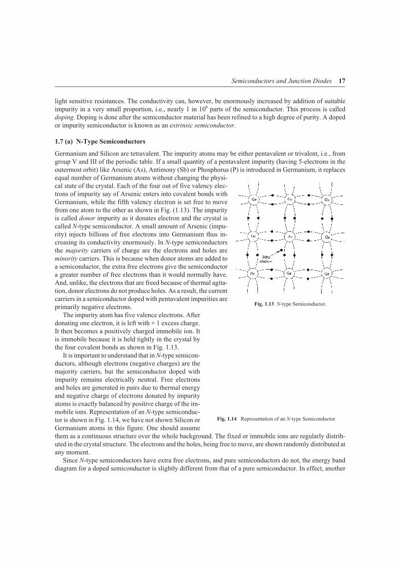
1.7 (a) N-Type Semiconductors
Germanium and Silicon are tetravalent. The impurity atoms may be either pentavalent or trivalent, i.e., fromgroup V and III of the periodic table. If a small quantity of a pentavalent impurity (having 5-electrons in theoutermost orbit) like Arsenic (As), Antimony (Sb) or Phosphorus (P) is introduced in Germanium, it replacesequal number of Germanium atoms without changing the physi-cal state of the crystal. Each of the four out of five valency elec-trons of impurity say of Arsenic enters into covalent bonds withGermanium, while the fifth valency electron is set free to movefrom one atom to the other as shown in Fig. (1.13). The impurityis called donor impurity as it donates electron and the crystal iscalled N-type semiconductor. A small amount of Arsenic (impu-rity) injects billions of free electrons into Germanium thus in-creasing its conductivity enormously. In N-type semiconductorsthe majority carriers of charge are the electrons and holes areminority carriers. This is because when donor atoms are added toa semiconductor, the extra free electrons give the semiconductora greater number of free electrons than it would normally have.And, unlike, the electrons that are freed because of thermal agita-tion, donor electrons do not produce holes. As a result, the currentcarriers in a semiconductor doped with pentavalent impurities areprimarily negative electrons.
The impurity atom has five valence electrons. Afterdonating one electron, it is left with + 1 excess charge.It then becomes a positively charged immobile ion. Itis immobile because it is held tightly in the crystal bythe four covalent bonds as shown in Fig. 1.13.
It is important to understand that in N-type semicon-ductors, although electrons (negative charges) are themajority carriers, but the semiconductor doped withimpurity remains electrically neutral. Free electronsand holes are generated in pairs due to thermal energyand negative charge of electrons donated by impurityatoms is exactly balanced by positive charge of the im-mobile ions. Representation of an N-type semiconduc-tor is shown in Fig. 1.14, we have not shown Silicon orGermanium atoms in this figure. One should assumethem as a continuous structure over the whole background. The fixed or immobile ions are regularly distrib-uted in the crystal structure. The electrons and the holes, being free to move, are shown randomly distributed atany moment.
Since N-type semiconductors have extra free electrons, and pure semiconductors do not, the energy banddiagram for a doped semiconductor is slightly different from that of a pure semiconductor. In effect, another
Semiconductors and Junction Diodes 17
Fig. 1.13 N-type Semiconductor.
Fig. 1.14 Representation of an N-type Semiconductor.

energy level exists; a level for the donor electron,which is closer to the conduction band. The for-bidden band for the donor electron is much nar-rower than the forbidden band for the valenceelectron; so one can see that it is much easier tocause electron flow in an N-type semiconductor(Fig. 1.15).
1.7 (b) P-type Semiconductor
When a trivalent impurity (having 3 electrons inoutermost orbit) like Indium (In), Boron (B) or Gallium (Ga) is added in a Germanium intrinsic semiconduc-tor, the impurity atoms will displace some of the Germanium atoms in the crystal during its formation asshown in Fig. 1.16. In this case only three out of the four possible covalent bonds are filled while the fourthbond is vacant and the vacancy acts as a hole. Hence a hole moves relative to the electron in a direction oppo-site to the direction of electron, when an electron moves from one bond to the other. This trivalent impurityknown as the acceptor or P-type impurity injects into the crystal billions of holes and the majority carriers ofthe charge are the holes responsible for the conductivity of the crystal. For this reason such crystals are calledP-type semiconductors or P-type crystals. P-type semiconductor can be represented as shown in Fig. 1.17.
The energy band diagram of P-type semiconduc-tor also differs from that of the pure superconductor.Since there is an extra number of holes, which tendto attract electrons, they aid in starting current flow.As a result, the acceptor energy level is also some-what higher than that of the valence band. However,it is not as high as the donor level (Fig. 1.18a).P-type semiconductors will conduct easily than puresemiconductors, but not quite as easy as n-typesemiconductors.
18 Electronics—Theory and Applications
Fig. 1.15 Excess Free Elections in N-type Semiconductors Producea Donor Energy Level Close to the Conduction Band.
Fig. 1.16 P-type Semiconductor. Fig. 1.17 Representation of a P-type Semiconductor.
Fig. 1.18 (a) Excess Holes in P-type Semiconductors Introducean Acceptor Energy Level Close to Valence Level.

1.8 Important Properties of Extrinsic Semiconductors
We have seen that the introduction of impurities in pure semiconductors increases the density of one type oranother type of charge carriers. The product of holes and electrons in a semiconductor is constant dependingon the width of energy gap and temperature and hence the introduction of the impurities results in an increasein the density of one type of carrier and a reduction in the density of the other type of carrier. In an extrinsicsemiconductor, the carriers introduced by the impurities are called majority carriers and the other type arecalled minority carriers. It is important to note that the low value for minority carrier density is due to added re-combination.
Let Nd be the donor impurity density, Na the acceptor impurity density, p the density of holes and n thedensity of electrons in an extrinsic semiconducting material. From the condition of charge neutrality, we have
Nd + p = Na + n
or n N N p N Nn
nnp nd a d a
i
i= − + = − + =( ) ( ) ( )
22
or n N N n nd a i
2 2 0− − − =( ) (1.16)
Solving the quadratic equation in n, one obtains
or
nN N N N n
n N N N N n
d a d a i
d a d a i
=− ± − +
≈ − − >>
( ) ( )
( ) ( )
2 24
2when
(1.17)
Obviously, the electron density (n) in the N-type semiconductor equals the difference in the donor and ac-ceptor impurity densities when they are large compared to the intrinsic density, ni,. Similarly the hole density(p) in a P-type semiconductor is given by
p = (Na – Nd) when (Na – Nd) >> ni
1.8 (a) Donor and Acceptor States
When an impurity atom from group V of the periodic table, say Phosphorous is added to a pure Ge or Si crystalas a pentavalent impurity, these impurity atoms enter the lattice by substitution for normal atoms, and not ininterstitial positions. These impurity atoms contribute five electrons per atom to the valence band, i.e. we havean extra electron per impurity atom. These additional electrons (which cannot be accommodated in thevalence band of the original lattice) occupy some discrete energy levels just below the conduction band; theseparation may be a few tenths of an electron volt. These excess electrons are released by the impurity atomsand excited into the conduction band. The excited electrons then contribute to the electrical conductivity of thesemiconductor. Conversely, the impurity may consist of atoms having fewer electrons than of a semiconduc-tor [Fig. 1.18(b)]. For the cases in which Si and Ge are the host substances, the impurity atoms could be boronor aluminium, each of which contributes only three electrons. In this situation the impurity introduces vacantdiscrete energy levels, very close to the top of the valence band. Therefore it is easy to excite some of the moreenergetic electrons in the valence band into the impurity levels. This process produces vacant states, or holes,in the valence band. These holes then act as positive electrons [Fig. 1.18(c)]. We must note that to produce sig-nificant changes in the conductivity of a semiconductor, it is sufficient to have about one impurity atom permillion semiconductor atoms.
We have already seen that the crystal as a whole remains neutral because the electron remains in the crys-tal. We have further seen that the band diagram of N-type or P-type semiconductor differs from that of the pure
Semiconductors and Junction Diodes 19

semiconductor. The band diagram for N-type or P-type semiconductor explains clearly why the conductionbecomes possible in impure semiconductors at comparatively low temperatures.
1.8 (b) Fermi Level in Extrinsic Semiconductor
We have read that Fermi level is situated in the middle of the band gap in an intrinsic semiconductor as theelectron and hole densities are equal. When the intrinsic semiconductor is doped, the carrier densities change,consequently the position of the Fermi level also changes. The shift in the position of the Fermi level can easilybe related to the majority carrier density in an extrinsic semiconductor if it is assumed that the addition of im-purities do not affect the densities of energy states in the conduction and valence bands.
Let Nc and Nv denote the density of states in the conduction band and density of states in the valence band,respectively. We have for an intrinsic semiconductor
and
n NE E
kT
p NE E
kT
cfi c
v
c fi
=−
=−
exp
exp
(1.18)
Here Efi is the energy associated with the Fermi level in an intrinsic semiconductor. For an intrinsic semicon-ductor, we have n = p and therefore from (1.18), we have
N
N
E E E
kT
c
v
c v fi=− −
exp
2
Let Efn be the energy associated with the Fermi level in an N-type semiconductor having an electron densityn, we have
n NE E
kTc
fn c=−
exp
and p NE E
kTc
v fn=−
exp
∴ n
p
n
n
N
N
E E E
kT
E E
kTi
c
v
fn c v fn fi= =− −
=
−2
2
2 2exp exp
( )
or n nE E
kTi
fn fi=−
exp (1.19)
20 Electronics—Theory and Applications
Fig. 1.18 Impurities in a semiconductor (b) Donors, or N-Type (c) Acceptors, or P-Type

Similarly, one obtains for a p-type semiconductor
p nE E
kTi
fi fi=−
exp (1.20)
Thus the shift in the Fermi level in the n
and p type of semiconductor can be ex-pressed as
E E kTn
n
E E kTp
p
fn fi
i
fi fp
i
− =
− =
ln
ln
(1.21)
Fig. 1.19 represents the shift in theFermi level in the N- and P-types of semi-conductors.
1.8 (c) Thermal Ionization of Extrinsic Semiconductors
When the temperature of an extrinsic semiconductor is raised above 0°K, the impurity atoms get ionized. Dueto ionization the donor impurity atoms give rise to electrons in the conduction band and the acceptor impurityatoms give rise to holes in the valence band. These electrons or holes alongwith those generated by intrinsicaction, then serve as the current carriers at a temperature. Two cases of interest are
(i) Conduction electron concentration is equal to
n = n0 exp [(EF – Eg)/kT] ≈ Nd (1.22)
This shows that under the present conditions the concentration of conduction electrons is approxi-mately equal to the concentration of donors. This means that all the donors are ionized. Equation(1.22) suggests that at room temperature the impurity concentration for Si and Ge upto 1014 to 1016 do-nors per cc suits this range, i.e., if we dope an intrinsic semiconductor crystal with this concentrationof donors, one can certainly predict that one will have ~1016 electrons/cc.
(ii) At higher temperature, the carrier concentration is proportional to N d .
1.8 (d) Charge Densities in Extrinsic Semiconductors
The density of impurity atoms in N- and P-materials is so low compared to the density of semiconductor atomsthat the rate of thermal pair generation is not affected appreciably by the presence of impurity atoms. In thecase of intrinsic semiconductors we have seen that the concentration product
np ni
= 2 [1.22(a)]
was a constant at a given temperature.Assuming all impurity atoms in extrinsic semiconductors to be ionized at the usual operating temperatures,
the free charge densities in impurity material can be based upon ND, the donor atom density in N-material, orNA, the acceptor atom density in P-material.
The electrical neutrality of the material demands
p = ND = n + NA [1.22(b)]
Semiconductors and Junction Diodes 21
Fig. 1.19 Shift in the Fermi level in the N- and P-type of Semiconductors.
The L.H.S. of equation 1.22(b) gives the total positive charge as the sum of holes in the valence bonds andthe positive charge associated with the donor atoms that have given up electrons and become positive ions.The R.H.S. of equation 1.22(b) sums the negative charge of free electron density n and the negative charge dueto electrons held by the ionized acceptor atoms.
Using 1.22(a), one can write
nn
pp
n
n
i i= =2 2
and [1.22(c)]
only donor impurities are introduced in N-type material, so NA = 0. The donor density will be made muchlarger than the density of intrinsic holes, or
ND >> p
and in N-type material the electron density is written from equation 1.22(b) as
n ≅ ND [1.22(d)]
on the similar reasoning for P-type material, we have ND = 0 and NA >> n. One obtains density relations inP-type material as
nn
N
i
A
≅2
[1.22(e)]
p N A≅ [1.22(f)]
From the above results we can conclude that the density of majority carrier approximates the impurity atomdensity at usual ambient temperatures, and the density of minority carriers is reduced below the intrinsic level.This means that the increased electron density in N-type material raises the probability that an electron willmeet and recombine with a hole, and so the hole density is decreased to maintain n2 constant.
1.9 Semiconductor Devices
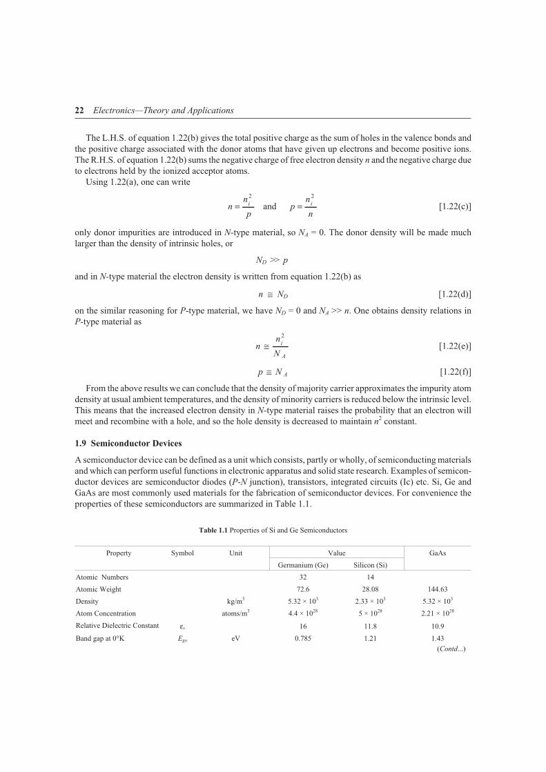
A semiconductor device can be defined as a unit which consists, partly or wholly, of semiconducting materialsand which can perform useful functions in electronic apparatus and solid state research. Examples of semicon-ductor devices are semiconductor diodes (P-N junction), transistors, integrated circuits (Ic) etc. Si, Ge andGaAs are most commonly used materials for the fabrication of semiconductor devices. For convenience theproperties of these semiconductors are summarized in Table 1.1.
Table 1.1 Properties of Si and Ge Semiconductors
Property Symbol Unit Value GaAs
Germanium (Ge) Silicon (Si)
Atomic Numbers 32 14
Atomic Weight 72.6 28.08 144.63
Density kg/m3 5.32 × 10³ 2.33 × 10³ 5.32 × 10³
Atom Concentration atoms/m3 4.4 × 1028 5 × 1028 2.21 × 1028
Relative Dielectric Constant εr 16 11.8 10.9
Band gap at 0°K Ego eV 0.785 1.21 1.43
22 Electronics—Theory and Applications
(Contd...)

Property Symbol Unit Value GaAs
Germanium (Ge) Silicon (Si)
Band gap at 300 K Eg eV 0.72 1.1 1.32
Intrinsic Carrier(generation) at 300 K ni
Carriers
m3
2.5 × 10¹⁹ 1.5 × 10¹⁶ 9.0 × 10¹²
Crystal Structure Diamond Diamond Zincblende
Lattice Constant a Å 5.65748 5.43086 5.6534
Melting Point °C 936 1420 1250
Minority Carrier life time second (s) ~10–3 ~2.5 × 10⁻³ ~ 10–8
Breakdown Field V/m ~107 ~ 3 × 10⁷ ~ 4 × 10⁵
Diffusion Constant Dn
(electrons) m2/s 0.009842 0.003367 0.001036
Dn (holes) 0.004662 0.001295 0.000906
Effective Density of states inthe conduction band Nc m–3 1.04 × 1025 2.8 × 1025 4.7 × 10²²
Effective Density of states inthe valence band Nv m–3 6.4 × 1024 1.02 × 1025 7.0 × 10²²
Intrinsic conductivity σi Sm–1 2.2428 0.4325 × 10⁻³ 1.2832 × 10⁻⁶
Mobility (Drift) at 300 K µn
(electron)m
2
V s− 0.38 0.13 0.85
µp
(holes)m
2
V s− 0.18 0.05 0.04
Work function W Volt (V) 4.4 4.8 4.7
Raman Phonon energy eV 0.037 0.063 0.035
Almost all semiconductor devices are comprised of a single crystal semiconductor incorporating two ormore semiconducting regions of different impurity density. The difference in the electric fields and carrierdensities associated with differently doped regions, called junctions, permit a wide range of essentially nonlin-ear conductivity effects in devices incorporating two, three or more distinct regions. Most semiconductordevices can be understood through the simplest of such junctions, called the P-N junction, which is a system oftwo semiconductors in physical contact, one with excess of electrons (N-type) and other with excess of holes(P-type.)
1.10 P-N Junction
When a P-type semiconductor is brougth into contact with N-type semiconductor as the process ofcrystallisation is taking place, the resulting combination is called a P-N junction. This junction has importantproperties and is, in effect, the basis of modern semiconductor theory and practice. Most semiconductordevices contain one or more P-N junction. The most important characteristic of a P-N junction is its ability toconduct current in one direction only. In the reverse direction it offers very high resistance.
Formation of a P-N Junction: Fig. 1.20 shows three types of such junctions. In Fig. 1.20 (a), P and N regionshave been grown into the germanium block by mixing acceptor and donor impurities, respectively, into thesingle crystal during its formation. This is known as a grown junction. It is worthwhile to mention that thegrown type of P-N Junction is not a sandwich made by attaching a P block to an N block, but actually consistsof P and N layers in a single piece of germanium.
Semiconductors and Junction Diodes 23

The diffused junction in Fig. 1.20 (b) is made by placing a pellet of acceptor impurity, such as indium, onone face of a wafer of N-type germanium and then heating the combination to melt the impurity. Under properconditions of temperature and time, a portion of the impurity metal will diffuse a short distance into the wafer,thereby creating a region of P-type germanium in intimate association with W-type bulk. This is also called analloyed junction or fusion-alloy junction from the fact that a small amount of pellet material alloys with thegermanium.
Fig. 1.20 (c) shows a point contact type. Here, a fine, pointed wire (catwhisker) makes pressure contactwith the face of an N-type germanium wafer. After assembly, the device is electroformed by passing ahigh-current surge momentarily across the junction of Wafer and Whisker. The heat generated during the shortinterval drives a few electrons from the atoms in the region of the point contact, leaving holes and thus con-verting into p-type a small volume of germanium immediately under and around the point.
Silicon P-N junction is produced in a similar manner. In most instances, the Silicon has been processed insuch a way as to make it P-type. To create the junction, an n-type material is either inserted at the proper point inthe crystal process or (in the diffused, junction process) an n-type material is later inserted into the body of P-typewafer. Like germanium diodes, silicon diodes also are produced both in junction and point contact types.
P-N Junction with no external voltage: Fig. 1.21 shows a P-N junction just immediately after it is formed.There is no external voltage connected to the P-N junction. Since N-type material has a high concentration offree electrons while P-type material has a high concentration of holes, the following processes are initiated:
(i) At the junction, holes from the P region diffuse into the N region and free electrons from the N regiondiffuse into the P region. This process is called diffusion. Holes combine with the free electrons in theN-region whereas electrons combine with the holes in the P-region.
(ii) The diffusion of holes from P region to N region and electrons from N region to P region across thejunction takes place because they move haphazardly due to thermal energy and also because there is a
24 Electronics—Theory and Applications
Fig. 1.20 Types of P-N Junction.
Fig. 1.21 A P-N Junction When Just formed.

difference in their concentrations (The P region has moreholes whereas N region has more free electrons) in the tworegions.
(iii) As the free electrons move across the junction from N typeto P type, positive donor ions are uncovered, i.e., they arerobbed off free electrons. Hence a positive charge is builton the N-side of the junction. At the same time, the freeelectrons cross the junction and uncover the negativeacceptor ions by filling in the holes. Therefore, a net nega-tive charge is established on P-side of the junction. Whena sufficient number of donor and acceptor ions is uncov-ered, further diffusion is stopped. It. is because now, a bar-rier is set up against further movement of charge carriers.This is called potential barrier or junction barrier. Thepotential barrier is of the order of 0.1 to 0.3 volt. Fig. 1.22shows the electrostatic potential difference across the P-N
junction. How this potential barrier is developed? When asufficient number of donor and acceptor ions is uncov-ered, further diffusion is prevented. It is because now pos-itive charge (ions) on N-side repels holes to across from P
type to N type and negative charge (ions) on N-side repelsfree electrons to enter from N type to P type. Because ofthis a difference in potential exists between the two sec-tions, which inhibits further electron-hole combinations atthe junction, and the Fermi level of the two sides is in thesame level as shown in Fig. 1.22 (c).
(iv) The region across the P-N junction in which the potentialchanges from positive to negative is called the depletion region. The width of this region is of the order
of 6 × 10⁻⁸ m. Since this region has immobile (fixed) ions which are electrically charged, it is alsocalled as the space-charge region. Outside this region on each side of the junction, the material is stillneutral.
(v) The potential barrier for a silicon P-N junction is about 0.7 V, whereas for a germanium P-N junctionit is approximately 0.3 V.
The potential barrier discourages the diffusion of majority carriers across the junction. However, the potentialbarrier helps minority carriers (few free electrons in the P region and few holes in the N region) to drift acrossthe junction. The minority carriers are constantly generated due to thermal energy. But electric current cannotflow since no circuit has been connected to the P-N junction.
Width of Depletion Layer and Height of Potential Barrier: Let x1 and x2 be the width of depletion layer in P
and N sides respectively of a P-N diode junction, then total width of depletion layer
x = x1 + x2
Similarly if V1 and V2 are the potential barriers in P and N sides of P-N junction, then the net junction potentialbarrier (Fig. 1.22b).
V0 = V1 + V2
Semiconductors and Junction Diodes 25
Fig. 1.22 Potential barrier across the P-N junc-tion.
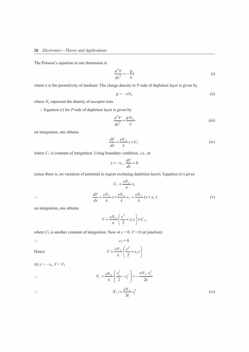
The Poisson’s equation in one dimension is
d V
dx
2
2= − ρ
ε1 (i)
where ε is the permittivity of medium. The charge density in P-side of depletion layer is given by
ρ = – eNa (ii)
where Na represent the density of acceptor ions.
∴ Equation (i) for P-side of depletion layer is given by
d V
dx
N a2
2= ρ
ε(iii)
on integration, one obtains
dV
dx
eNx C
a= +ε 1 (iv)
where C1 is constant of integration. Using boundary condition, i.e., at
x xdV
dx= − =1 0,
(since there is, no variation of potential in region exclusing depletion layer). Equation (iv) gives
CeN
xa
1 1=ε
∴ dV
dx
eNx
eNx
eNx x
a a a= + = +ε ε ε1 1( ) (v)
on integration, one obtains
VeN x
x x Ca= +
+
ε
2
1 22
,
where C2 is another constant of integration. Now at x = 0, V = 0 (at junction)
∴ c2 = 0
Hence VeN x
x xa= +
ε
2
12
At x = – x1, V = V1
∴ VeN x
xeN x
a a
112
12 1
2
2 2= −
= −
ε ε
∴ | |VeN
xa
1 12
2=
ε(vi)
26 Electronics—Theory and Applications

If Nd is density of donor ions in N-side of depletion layer, then Poission’s equation for this becomes
d V
dx
eNeNd
d
2
2= − = − =ρ
ε ερ( ) (vii)
Proceeding as above and applying boundary conditions that at x = 0,
V x xdV
dxV V= = = =0 02 2and at one obtains, , ,
VeN xd
222
2=
ε(viii)
∴ The height of the potential barrier across the junction is obtained as
V V V eN x N xa d
0 1 212
22
2= + =
+
| | | |ε
(ix)
Since the crystal as a whole is electrically neutral, the number of both sides of charge carriers must be equal, i.e.
N x A N x Aa d1 2=
where A is the area of crystal
∴ x
x
N
N
d
a
1
2
= (x)
or xN
Nx
a
d
2 1=
Substituting the value of x2 in (ix), one obtains
VN
xN
N
a a
d
0 12
21= +
εε
This gives xV
N N N
V
e
N N
N Na d
a d
a d
10
0
1
202
1
2=+
=
+ε
εε
( / )
( / )
( )
1
2
and xV
eN N N
V
e
N N
N Nd d a
a d
a d
20
1
202
1
2=+
=
+ε ε
( / )
( / )
( )
1
2
x x xV
e
N N
N N
N Nd a
a d
a= + =
=+
+1 20
1
2
1
22ε ( / )
( )
( / d
a dN N
)
( )+
1
2
or xV
e
N N
N N
a d
a d
=
+
2 0
1
2
1
2ε(xi)
Semiconductors and Junction Diodes 27

Width of the depletion region changes as square root of the voltage. In order to exemplify the order of thick-ness commonly met with, let us consider the example of Germanium PN diode in which Nd = 1021/m3 and
Na = 1023/m3. For these concentrations across the junction V0 = 0.31 volt, and since for Germanium εr = 16
(Here ε = εr ε0), one finds that the width of the unbiased junction is x = 0.75 × 10⁻⁶ m or 0.75 micron. We mustnote that in this numerical example Na >> Nd. Obviously, Eq. (xi) reduces to
xV
e N d
=
2 0
1
2ε(xii)
This shows that heavier doping on the side of junction extends the depletion layer to the other side. More-over, the depth of penetration or the width of the depletion region varies inversely as the square root of dopingdensity on the opposite side.
Because of the presence of space charges of opposite kinds across the junction there is a voltage gradientconfined within the depletion region. Obviously, the transition region thus acts like a parallel plate capacitor inwhich plates are separated by the distance x. The junction capacitance is thus
CdQ
dV xAJ = = ε
Farad (xiii)
where A is the area of the junction. Substituting (x) from (xi), one obtains
C
A
e
V
N N
N N m
J a d
a d
=+
ε2 0
1
2
2
Farad(xiv)
For a special case, i.e. for Na >> Nd, Eq. (xiv) reduces to
C
A
e
VNJ
d=
ε2 0
1
2(xv)
For the junction of 0.75 µ in the above numerical example the junction capacitance from Eq. (xiii) or by substitut-ing Eq. (xii) in Eq. (xiii), one obtains
C
A
e
VNdJ =
ε2 0
1
2(xvi)
For the junction width of 0.75 µ in the above numerical problem the junction capacitance from Eq. (xiii)
works out as CJ/A = 189 µF/m2 or 18.9 m µF/cm2. In a typical case if the junction area is A = 10–3 cm2, then weobtain its capacitance CJ = 18 pF.
Effect of Temperature on Barrier Voltage: The barrier voltage depends on doping density and temperature.For a given junction the doping density remains constant; therefore barrier voltage depends on temperature.With the rise in temperature, more minority charge carrier’s are produced, leading to their increased driftacross the junction. Consequently the equilibrium occurs at a slightly lower barrier potential. Obviously, thebarrier potential decreases with rise of temperature. It is found that for both germanium and siliconsemiconductors
∆ V0 – 2t m V
Here t°C denote the change in temperature, i.e. barrier potential decreases by about 2 mV per degree C.
28 Electronics—Theory and Applications

1.11 Forward and Reverse Biasing
(i) Forward Biasing
We have seen that the natural tendency of the majority carriers (free electrons in the N-section and holes in theP-section) was to combine at the junction. This is how the depletion region and potential barrier were formed.Actually, the combination of electrons and holes at the junction allows electrons to move in the same directionin both the P and N sections. In the N-section, free electrons move toward the junction; in the P section, for theholes to move toward the junction, valence electrons move away from the junction. Therefore, electron flow inboth the sections is in the same direction. This, of course, would be the basis of current flow.
With the P-N junction alone, the action stops because there is no external circuit and because of the poten-tial barrier that builds up. So, for current to flow, a battery can be connected to the diode to overcome thepotential barrier. And the polarity of the battery should be such that the majority carriers in both sections aredriven toward the junction. When the battery is connected in this way, it provides forward bias, causing for-
ward or high current to flow, because it allows the majority carriers to provide the current flow.To apply forward bias, positive terminal of the battery is connected to P type and negative terminal to N
type as shown in Fig. 1.23. The applied forward potential establishes an electric field which acts against thepotential barrier field. Obviously, the resultant field is weakened and the barrier height is reduced at the P-N
Semiconductors and Junction Diodes 29
Fig. 1.23 P-N Junction Showing Forward Bias.

junction, Fig. 1.23 (b) and (c). Since potential barrier height is very small (~ 0.2 V) and hence a small forwardvoltage is sufficient to completely eliminate the barrier. Obviously, at some forward voltage the potential bar-rier at the P-N junction can be eliminated altogether. Then the junction resistance will become almost zero,and a low resistance path is established for the entire circuit. Thus a large current is generated in the circuiteven for the small potential difference applied. Such a circuit is called forward bias circuit and the current iscalled forward current. The salient features of the forward bias circuit are summarized below:
(i) At some forward voltage, the potential barrier is eliminated altogether.
(ii) The P-N junction offers low forward resistance (rf) to current flow.
(iii) The magnitude of current in the circuit due to the establishment of low resistance path depends uponthe applied forward voltage, and it reduces as the voltage is increased there by forward current in-creases (Fig. 1.28). It is given by
I I ev VT= −0 1( )/ η (i)
where V = applied voltage
VT
T =11600
here T = Temperature in Kelvin
η = 1 for Ge and 2 for Si
The mechanism of current flow in a forward biased P-N junction is as follows:
(i) The free electrons from the negative battery terminal continue to arrive into the N-region while thefree electrons in the N-region move towards the P-N junction.
(ii) The electrons travel through the N-region as free electrons. Obviously, current in N region of theP-N junction is by free electrons.
(iii) When these free electrons reach the P-N junction, they combine with holes and become valence elec-trons. Since a hole is in the covalent bond and hence when a free electron combines with a hole, it be-comes a valence electron.
(iv) Current in the P region is by holes. Theelectrons travel through P-region as va-lence electrons.
(v) These valence electrons after leaving thecrystal, flow into the positive terminal ofthe battery.
The current flow in a forward biased P-N junc-tion is illustrated in Fig. 1.24.
(ii) Reverse Biasing
We have seen that for forward current flow, the battery must be connected to drive the majority carrierstowards the junction, where they combine to allow electrons to enter and leave the P-N junction. If the batteryconnections are reversed, the potential at the N side will draw the free electrons away from the junction, andthe negative potential at the P side will attract the holes away from the junction. With this battery connection,then, the majority carriers cannot combine at the junction, and majority current cannot flow. For this reason,when a voltage is applied in this way, it is called reverse bias.
However, reverse bias can cause a reverse current to flow, because minority carriers are present in thesemiconductor sections. Remember, that although the P section is doped to have excess holes, yet someelectrons are freed because of thermal agitation. Also, although the N section is doped to have excess free
30 Electronics—Theory and Applications
Fig. 1.24 Current Flow under Forward Bias.
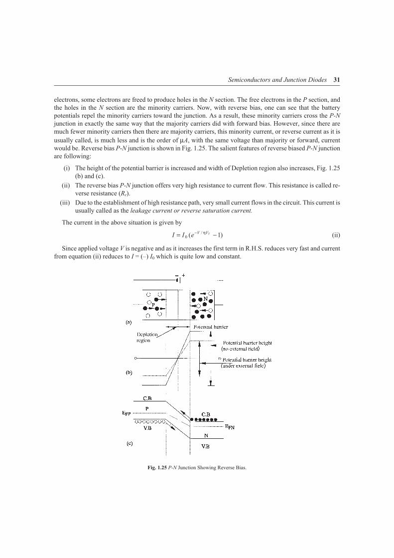
electrons, some electrons are freed to produce holes in the N section. The free electrons in the P section, andthe holes in the N section are the minority carriers. Now, with reverse bias, one can see that the batterypotentials repel the minority carriers toward the junction. As a result, these minority carriers cross the P-N
junction in exactly the same way that the majority carriers did with forward bias. However, since there aremuch fewer minority carriers then there are majority carriers, this minority current, or reverse current as it is
usually called, is much less and is the order of µA, with the same voltage than majority or forward, currentwould be. Reverse bias P-N junction is shown in Fig. 1.25. The salient features of reverse biased P-N junctionare following:
(i) The height of the potential barrier is increased and width of Depletion region also increases, Fig. 1.25(b) and (c).
(ii) The reverse bias P-N junction offers very high resistance to current flow. This resistance is called re-verse resistance (Rr).
(iii) Due to the establishment of high resistance path, very small current flows in the circuit. This current isusually called as the leakage current or reverse saturation current.
The current in the above situation is given by
I I eV VT= −−
0 1( )/ η (ii)
Since applied voltage V is negative and as it increases the first term in R.H.S. reduces very fast and currentfrom equation (ii) reduces to I = (–) I0 which is quite low and constant.
Semiconductors and Junction Diodes 31
Fig. 1.25 P-N Junction Showing Reverse Bias.

1.12 Volt-Ampere Characteristics of P-N Junction
The P-N junction can be represented by a symbol of arrow and dash asshown in Fig. 1.26. The arrow head represents the P-section of the crystaland shows the direction of flow of holes or conventional current. Since theP-N junction diode’s resistance changes according to the direction of currentflow and hence it is called a nonlinear device. Basically, its nonlinearity isdependent on the polarity of the applied voltage. For current in the forwarddirection, it has a resistance of only a few hundred ohms. In the reverse di-rection, its resistance is often close to 100,000 ohms.
Fig. 1.27 shows the circuit arrangement for drawing the V-I characteris-tics of a P-N junction diode.
A graph between the potential difference across the P-N junction and thecurrent through the junction is called the V-I characteristic of the P-N junc-tion diode and is shown in Fig. 1.28.
In the forward direction, though considerably more current flows and thecurrent for the most part, increases linearly as the bias voltage is increased.In the forward direction, then, the P-N junction can be considered a linear de-vice over a large portion of its operating curve. The small portion of thecurve that is just above zero bias is nonlinear. This results because both ma-jority and minority current actually comprise the overall current. Since theminority carriers are low energy carriers, majority current starts first, andthen as the voltage is raised, minority current joins in,causing a nonlinear rise in current. But as the voltage isincreased further, minority current becomes saturatedsince there are only few minority carriers. The curvethen follows the majority current increase which islinear.
Because of the non-linearity of the curve, if a verysmall signal voltage is applied to the diode so that itonly operates around the knee, the signal will be dis-torted. The signals must be large enough so that theyoperate mostly over the linear part of the curve.
When reverse bias is applied, a slight reverse cur-rent flows. This reverse current increases only negli-gibly as the bias voltage is increased a lot (20 to 25volts). At this stage current suddenly rises in the re-verse direction due to the breakdown of the crystal,i.e., covalent bonds of the crystal are broken in verylarge number. This breakdown reverse bias is called the Breakdown or zener voltage. Diodes are also de-signed to produce a useful wide range of zener breakdown region, and are used in special voltage-regulat-ing circuits. We will discuss zener diodes later on.
1.13 Static and Dynamic Resistance of a Diode
One of the most important properties of the diode is its resistance in the forward and reverse biasing. An idealdiode must offer zero resistance in forward bias and infinitely large resistance in reverse bias. Truly speaking,
32 Electronics—Theory and Applications
Fig. 1.26 Symbol of the P-N Junc-tion Diode.
Fig. 1.27 Circuit Arrangement forDrawing V-I Character-istics of a P-N Junction.
Fig. 1.28 V-I Characteristics of a P-N Junction Diode.

no diode can act as an ideal diode, i.e., an actual diode does not behave as a perfect conductor when forwardbiased and as a perfect insulator when reverse biased. We consider the two resistances of the diode
(i) d.c. or static resistance
(ii) a.c. or dynamic resistance
(i) d.c. or static resistance: When P-N junction diode is forward biased, it offers a definite resistance in thecircuit. This resistance is called as the dc or static resistance (RF) of the diode, dc resistance of diode is simplythe ratio of the dc voltage across the diode to the dc current flowing through it at a particular instant.
RV
IF =
(ii) a.c. or dynamic resistance: The ac or dynamic resistance of a diode, at a particular dc voltage, is equal tothe reciprocal of the slope of the characteristic at that point, i.e.,
rV
f = =change in voltage
resulting change in current
∆∆I
It is not a constant quantity but depends on operating voltage. For forward bias greater than the internaljunction voltage, the dynamic resistance varies inversely with the current, but for reverse bias its value is muchlarger.
Under forward bias for large applied voltage, the diode current at junction temperature T is given as
I IeV
kT=
−
0 1exp
η
where η = 1 for Ge and 2 for Si. Differentiating the above w.r.t. V, one obtains
dI
dVI
e
kTe I
e
kT
eV kT=
=
0 η η
η/
∴ rdV
dI
kT
Ie
k
e
T
If = = =
= ××
−
η η
η 1.38
1.6
10
10
23
19
–
T
I
or rf = 8.625 × 10⁻⁵ η (T/I).
1.14 Space Charge (or Depletion Region) Capacitance
When no external voltage is applied, the width (d) of the depletion region of a P-N junction diode comes out tobe about 5 × 10⁻⁷ m and is mostly in the N-type material. The movement of majority carriers i.e. holes and elec-trons across the junction causes opposite charges to be stored at this distance ‘d’ apart. This is effectively a par-allel plate capacitor whose capacitance CT (often called space-charge capacitance) is approximately 20 pFwith no external bias.
As forward bias is applied the depletion region decreases and the capacitance (CT) increases. Underreverse-bias conditions, the depletion region increases and CT decreases. This property of voltage variablecapacitance is made use in varactors, varicaps or voltacaps.
Semiconductors and Junction Diodes 33

Space Charge or Transition Capacitance: The thickness of depletion layer changes with voltage appliedacross the junction. Reverse biasing of a P-N junction, causes majority carriers to move away from thejunction, therefore uncovering more immobile charges. This increases the thickness of depletion layer.Similarly the forward biasing of a P-N junction decreases the amount of uncovered charge and hence thethickness of depletion layer. This change in the uncovered charge with the applied voltage may beconsidered as a capacitive effect. It gives rise to transition capacitance or junction capacitance CT, givenby
CdQ
dV
A
xT = = ε
Here x is thickness of depletion layer and A is junction cross-sectional area.One can show that the width x of depletion layer is given by
xV
e
N N
N N
a d
a d
= +
2 0
1
2ε
∴ Ce
V
N N
N NAT
a d
a d
=+
ε2 0
1
2
or C VT ∝0
1 2– /
Obviously, the transition or junction capacitance is not constant but depends on applied voltage and hence it isalso known as voltage-variance capacitance.
Diffusion or Storage Capacitance CD: When forward biased the P-N junction develops a dominating diffusioncapacitance CD. This arises due to injected charge stored near the junction outside the transition region and isdefined as the rate of change of injected charge with applied voltage, i.e.,
CdQ
dVD =
CD is found to be proportional to current (I) and is much larger than the CT CD has larger value in forward direc-tion and smaller value in reverse direction. The value of CD in forward direction varies from 500 pF to 200 pF.Obviously, CD predominates under forward bias and arises due to minority carriers, while CT predominatesunder reverse bias and arises due to majority carriers.
1.15 Effect of Temperature on P-N Junction Diodes
We know that temperature rise boosts the generation of electron-hole pairs in semiconductors and increasestheir conductivity. From a consideration of the energies of the carriers crossing the depletion region in a P-N
junction diode, an involved calculation yields the following relation between diode current, voltage and tem-perature: (see Appendix D)
I = I0 exp [V/η VT – 1] (1.23)
Here
I = the diode current (forward if positive, reverse if negative)I0 = the diode reverse current, also called the reverse saturation current, at temperature T.
V = the diode voltage, positive for forward bias, negative for reverse bias; in volts.
34 Electronics—Theory and Applications

η = 1 for germanium and 2 for silicon.VT = T/11600, a quantity in volts, dependent upon temperature and is known as volt temperature equiva-
lent.T = Temperature of the diode junction (°K)
On increasing the temperature the forward characteristic (Fig. 1.28) shifts to left, showing increase in currentfor same voltage and it shifts to right when temperature is decreased showing biased current.
1.16 Zener Diodes
We have seen that in the breakdown region, large changes in diode current produce only small changes in diodevoltage. So a semiconductor P-N diode designed to operate in the breakdown, region may be employed as aconstant voltage device. The diodes used in such a manner are called avalanche breakdown or zener diodes.
They are used as a voltage regulator in the manner shown in Fig. 1.29 (b). The voltage source V and theresistance R are so selected that the diode operates in the breakdown region. The diode voltage in this regionwhich is also the voltage across the load RL is called zener voltage (Vz) and the diode current is called zener cur-rent (IZ). As the load current (IL) or the supply voltage changes, the diode accommodates itself to these changesand maintains nearly constant load voltage (Vz).
The diode will continue to regulate the voltage until the diode current falls to knee current Izk (Fig. 1.29)(c).Depending upon the nature of the semiconductor and its doping, the breakdown voltage in diode ranges from about3 volt to several hundred volts. The breakdown phenomenon is reversible and harmless so long as the safe operat-ing temperature is maintained.
The mechanism of diode breakdown at reverse voltage is explained below:
(i) Avalanche Breakdown. In this mechanism, the minority charge carriers (electrons in P type and holes in N
type) acquire sufficient energy from the applied reverse voltage to produce new charge carriers by removingvalence electrons from the covalent bonds. The new carriers in turn produce additional charge carriers and theprocess multiplies to give large reverse currents. The diode is then said to be in the region of avalanche
breakdown, usually, a junction with a broad depletion layer (therefore a low field intensity) breaks down bythis mechanism. With the increase of temperature, the vibrations of the atoms in the crystal increase whichincreases the possibility of collisions of the charge carriers with the lattice atoms and reduces the possibilityfor the carriers to gain sufficient energy to start avalanche process. Thus at high voltages, the avalancheprocess is prominent and does take place to cause diode breakdown. The operating voltages in such diodesrange from several volts to a few hundred volts.
Semiconductors and Junction Diodes 35
Fig. 1.29 (a) Symbol of Zener Diode, (b) Zener Diode as a Voltage Regulator.

(ii) Zener Breakdown. In this mechanism, the breakdown is initiated through a direct rupture of covalent bondsrather than avalenche process due to the existence of strong electric field across depletion layer. A junction
having a narrow depletion layer and hence high field intensity EV
d
r=
will break down by this mechanism.
An increase in temperature increases the energy of the valence electrons and makes it easier for these electronsto escape from these covalent bonds. Smaller applied voltage is, therefore, required to pull these electronsfrom the crystal lattice. The zener effect plays an important role only in diodes with breakdown voltage below
about 6 volts. The zener diode is always used in reverse biased condition (Fig. 1.29 (b)).The range of voltages about the breakdown voltage in which a zener diode conducts in reverse direction is
called tolerance.
We must note that during manufacturing, it is very difficult to have exact doping for every zener diode ofthe same number, i.e. type. Obviously, breakdown voltages of zeners of same number also differ slightly. Thisrange of breakdown voltages for the same type of zener diodes is referred as tolerance. Let us consider, for ex-ample, a particular type of zeners marked 9V, 10% tolerance. These zener diodes may have breakdown volt-age from 8.1V (9 – 0.9) to 9.9 V (9 + 0.9) instead of sharp 9V for all.
The breakdown voltage of zener diode depends upon operating temperature. It is found to decreasewith increase in junction temperature. This is due to the increased reverse current, (i.e. increase in minor-ity carriers) that flows with increasing temperature. The decrease in breakdown voltage is about 2 mV perdegree centigrade rise in temperature.
The maximum power which a zener diode can dissipate (or handle) without damage is referred as its power
rating and denoted by PZM. Zener diodes for the commercial purposes available in the market have power rat-ing from 1/4 W to more than 50 W.
Power rating (PZM) is the product of maximum current IZM which a zener diode can handle and the rated oroperating voltage of a zener diode (VZ), i.e.
P I VZM ZM Z=A data sheet, sometimes includes the maximum current rating of a zener diode. The maximum value of cur-
rent which a zener diode can handle at its rated voltage without damage is referred as its maximum current rat-ing (IZM).
When a Zener diode is operated in the breakdown region, as increase in current produces a slight increase involtage. This means that a zener diode has a small a.c. resistance. This a.c. resistance is called zener resistance(often referred as zener impedance ZZT). Sometimes, we find the specification about this resistance on the datasheets supplied by the manufactures.
The opposition offered to the current flowing through the zener diode in the operating region is known aszener resistance (RZ) or Zener impedance (ZZ).
Zener diodes find wide commercial and industrial applications, e.g. voltage stablizer, meter protection,wave shaping, etc.
1.16(a) Constant Current Diode
These are the diodes that work exactly opposite to Zener diode. These diodes keep the current constant flow-
ing through them when the voltage changes, i.e. instead of holding the voltage constant, these diodes hold thecurrent constant. The range of voltage over which a diode can keep the current constant is known as voltage
compliance. These diodes are optimised for a particular voltage compliance.
1.17 Tunnel Diode
It is a device just like a P-N junction, which offers negative resistance under certain bias conditions. The nega-tive resistance of the diode is due to tunneling and it is called a tunnel diode or Esaki diode. It is made very
36 Electronics—Theory and Applications

much like an ordinary P-N junction diode, except that both the P and N regions are heavily doped (1 : 104 )thousand times more than ordinary diode. It is used as an active device in electronic circuits in the frequencyrange of few megahertz. The semiconductors with very high impurity concentration are referred to as degener-ate semiconductors. Typical tunnel diode characteristic is shown in Fig. 1.29 (a).
As a result of high impurity levels, the contact potential ishigh, the depletion layer is very narrow and the Fermi levelslie in the conduction band for N-side and in the valence bandof the P side (Fig. 1.29 (b)). Under these circumstances, avery abrupt transition from P to N type material is achievedwithin the crystal. Since depletion region is very narrow; thisgives rise to extremely large electric fields.
Tunnel Effect. When a P-N semiconductor is heavily doped,(it has many majority carriers and ions), and under forwardbiased the hole and valence electron random drift is heavy.As a result, it is not uncommon for a large number ofelectrons to fill holes and release energy to only a few othervalence electrons. These few valence electrons, then, havetheir energy levels raised considerably so that they cancross from the N to the P section and current increases asshown by OA [F ig. 1.30a], even with little or no appliedvoltage. This action which seems to allow a valenceelectron to cross a potential barrier without enough appliedexternal energy is called the tunnel effect because it seemsas though the valence electron ‘tunnels’ through theforbidden band as shown in Fig. 1.30 (c). On furtherincreasing voltage the barrier height decreases (Fig. 1.30(d)) and Fermi level EFN is much raised so current decreasesas shown by AB (Fig. 1.30 (a)). This region is callednegative resistance region. On further increasing voltagethe conduction band of N type is in level with C B of P type
Semiconductors and Junction Diodes 37
Fig. 1.30(a)
Fig. 1.30 (b–e) Tunnel Diode—Characteristics andEnergy Levels.

and free electrons of N type easily cross toP type thereby current BC again increaseslike ordinary diode as shown by BC (Fig1.30a).
The negative resistance region AB (Fig.1.30) allows the diode to be used as anoscillator. It can also be used as an elec-tronic switch since it has a good responsein negative resistance region. By its nature,the tunnel diode has a rather high reversecurrent, but operation under this conditionis not generally used.
The equivalent circuit of tunnel diode is as shown in Fig. 1.31. The series resistance RS is the ohmic resis-tance. The series inductance LS depends upon the lead length and geometry of the diode package. The junctioncapacitance C depends upon the bias and is usually measured at the valley point. The negative resistance [– Rn]has a minimum at the point of inflection between peak current Ip and valley current Iv. Typical values for these
parameters for a tunnel diode having peak current value Ip = 10 mA are Rn = (–) 30 Ω, Rs = 1 Ω, Ls = 5 nH andC = 20 pF.
It is a voltage controllable device (like tetrode). Since between Ip and Iv we have three values of voltage fora given current and on account of its multivalued feature its is used in pulse and digital circuiting.
Our main interest in the tunnel diode is its application as a very high speed switch. Since tunneling takesplace at the speed of light, the transient response is limited only by total shunt capacitance (junction plus straywiring capacitance) and peak driving current. Switching times of the order of a nanosecond are reasonable andtimes as low as 50 p.secs have been obtained.
The advantages of a tunnel diode are (i) low cost,(ii) low noise, (iii) high speed, (iv) environmentalimmunity and (v) low power.
The disadvantages of the diode are its low outputvoltage swing and the fact that it is a two terminaldevice unlike ordinary diode in which current flowsonly when forward biased. Because of this latter fea-ture, there is no isolation between the input and out-put and it leads to serious circuit design problems.
However we may have a special type of tunneldiode whose peak value current is of the order ofvalley current. Such a diode is called Backward
Diode. V.I Characterstic of a backward diode isshown in Fig. 1.32. We may use it under reverse bi-ased condition as ordinary diode with the advantagethat now the diode current is available just beyondzero volt whereas in ordinary diode, current is notavailable till applied voltage is more than (breakover voltage) 0.7 volt in case of silicon and so in case a back diode it is conveniently used as rectifier for V
small (mV) input signals (For details of backward diode see section 1.23).
1.18 Photodiode
A photo-diode is a P-N junction diode packed into a transparent plastic packet working under reverse biasedcondition.
38 Electronics—Theory and Applications
Fig. 1.31 Equivalent Circuit of a Tunnel Diode.
Fig. 1.32 V-I Characteristic of Backward Diode.

Principle. A very small current flows through a P-N junction diode when it is reverse biased. It is because,minority charge carrier takes part in conduction. The number of minority carrier depend upon the workingtemperature. However when photons (light) of suitable frequency is incident on the junction, the number ofcharge carrier increases. But this happens only when light radiations such the junction which is not the case inordinary diode.
Working. In a photo diode visible light is focussed on the junction through a lens (Fig. 1.33). Light on beingincident produces free electrons and holes. Thus number of charge carriers increases and current increases.Generally a photodiode is optimized for its sensitivity to light. As the light intensity increases more and morecharge carriers are generated and reverse bias current increases Fig. (1.34).
In this respect a photodiode acts as a photo detector, a device which converts incoming light signal intoelectrical signal.
Volt-Ampere characteristic: Under normal reverse bias the current in a P-N junction diode is given by
I I e IV kT= − ≈ −−
0 01( )/ η
since applied voltage V is negative. So at higher values of V the first term goes to zero.On illuminating the diode under reverse biased conditions the number of hole-electrons pairs increases.
Which is proportional to the intensity of incident light (number of photons). Hence the total current flowingthrough the diode,
I = I0 + IS
where IS is the short circuit current generated on account of photoelectric effect. In general the volt-amperecharacteristic is given by
Semiconductors and Junction Diodes 39
Fig. 1.33 Equivalent Circuit of a Photo-diode. Fig. 1.34 V-I Characteristic of Photo-diode.

I I I eSV kT= + −−
0 1( )/ η (1.24)
This characteristic is drawn in Fig. 1.34.
Small Signal Model: Under ideal conditions a photo-diode under reverse biased condition is shown in Fig.1.35 (a). In Fig. 1.35 (b) parasitic elements C, R and r are taken into consideration, where R represents reversebiased resistance. C represents the transition capacitance and ‘r’ represents the bulk ohmic resistance. Thebarrier capacitance C is of the order of 10 pF, R ≈ 50 MΩ and r = 100Ω. In Fig. 1.34 the dark current I0
corresponds to the reverse current due to thermally generated electron- hole pairs. From equation (1.24) wesee that if diode terminals are open circuited then the total current I has be zero. Under such conditions, avoltage known as photovoltaic potential V0C will appear across diode. It is given by
V VI
Ioc T
s
o
= +
η ln 1 (1.25)
where VT is the volt equivalent of temperature and η is a constant equivalent to unity for Ge and 2 for Si.
Thus V0C increases logarithmically with Is or with intensity of incident light. Now if a load (RL) is connectedacross the diode, the voltage drop across it will correspond to incident light intensity. The output voltage gen-erated is of the order of few hundred millivolts across RL of few kilo-ohms. Large area photovoltaic P-N junc-tion banks have been used for conversion of solar energy into electrical energy which is the basis of solar cells.
1.18(a) Solar Cells
Solar cells, which convert the sunlight directly into electricity, at present furnish the most important long dura-tion power supply for satellites and space vehicles. These cells have also been successfully employed insmall-scale terrestrial applications. Today, the solar cell is considered a major device for obtaining energyfrom the sun. Since it can covert sunlight directly to electricity with high conversion efficiency, and can pro-vide nearly permanent power at low operating cost, and is virtually free of pollution. Recently, research andpollution development of low-cost, flat panel solar cells, thin film devices, concentrator systems, and manyinnovative concepts have increased. We can expect that in near future, the costs of small solar power modularunits and solar power plants will be economically feasible for large-scale use of solar energy.
The first solar cell were developed by chapin et al. in 1954 using a diffused silicon p-n function. Subse-quently, the cadmium-sulphide solar cell was developed by Raynolds et al. in 1954. To date, solar cells havebeen made of many other semiconductors, using various device configurations and employing single-crystal,polycrystal, and amorphous thin film structures.
40 Electronics—Theory and Applications
Fig. 1.35 Photo-diode under (a) Reverse Biased Condition, (b) Parasitic Elements.

Photo-voltaic Effect and Solar Cells
The photo-voltaic effect can be observed in nature in a variety of materials, but the materials that have shownthe best performance in sunlight are the semiconductors. In photovoltaic conversion, the solar radiation fallson devices called solar cells which convert the sunlight directly into electricity. The principal advantages asso-ciated with solar cells are that they have no moving parts, require little maintenance, and work quite satisfacto-rily with beam or diffuse radiation.
A typical schematic representative of a conventional silicon solar cell is shown in Fig. 1.35(a). Silicon cells
are thin wafers about 300 µm in thickness and 3 to 4 cm in diameter sliced from a single crystal of an type orp-type doped silicon. A shallow p-n function is formed at one end by diffusion. Metal electrodes made from aTi-Ag solder are attached to the front and back side of the solar cell. On the front and back side of the cell areattached metal electrodes made from a Ti-Ag solder. On the front side, the electrode is in the form of a metalgrid with fingers which permit the sunlight to go through, while on the backside, the electrode completely cov-
ers the surface. An antireflection contain of SiO having a thickness of about 0.1µm is also put on the top sur-face of the cell.
When a monochromatic radiation of wavelength λ is incident on the front surface of a cell, it is absorbedand pairs of positive and negative charges, called electron-hole pairs are created. The generation rate ofelectron-hole pairs at a distance x from the semiconductor surface is given by
G x F R x( , ) ( ) ( )[ ( )] exp[ ( ) ]λ α λ λ λ α λ= − −1 (1.26)
where α(λ) is the absorption coefficient F(λ) the number of incident photons/cm2/s per unit bandwidth, andR(λ) the fraction of these photons reflected from the surface. The positive and negative charges are separatedbecause of the p-n function. The direct current thereby produced is collected by the metal electrodes and flowsto the external load. The total photocurrent at a given wavelength is given by
J J J Jp n dr( ) ( ) ( ) ( )λ λ λ λ= + + (1.27)
where Jp and Jn are photo current densities due to holes and electrons respectively and Jdr is the photocurrentper unit bandwidth, representing photocurrent generation taking place within the depletion region.
Semiconductors and Junction Diodes 41
Fig. 1.35 (a) Schematic representation of a Silicon Solar Cell

The conversion efficiency the can be derived from the device is given by
η = I V
P
m m
in
(1.28)
where Vm and Im are the voltage and current at maximum power point and Pin is the power density of the sun-light. For Silicon cells, n range between 10 and 15 per cent. An important property of the material affecting theconversion efficiency is the hand gap energy (Eg). Photons of solar radiations having energy (E) less than theband gap energy are not usually absorbed. On the other hand, photons of sunlight having E > Eg have theirenergy partially utilized with the quantity (E – Eg) being wasted as heat. The value of Eg for Silicon is 1.20 eV.This value is quite close to the optimum value desirable from the stand point of obtaining maximumefficiency.
Apart from the band gap energy, the current voltage characteris-tic of a solar cell also influences its efficiency. Fig. 1.35(b) show atypical characteristic for a solar cell. The current Isc obtained at zerovoltage is called the short circuit current, while the voltage Voc
obtained with an open circuit is called the open circuit voltage. Theopen-circuit voltage Voc and the short-circuit current Isc are deter-mined for a given light level by the cell properties. The product ofthese quantities is the ideal power of the cell. The maximum usefulpower is the area of the largest rectangle that can be formed underthe I-V curve. Calling these values of voltage and current Vm and Im
We can see that the maximum delivered power illustrated by therectangle in the Figure 1.35(b) is less than Voc Isc product. The ratioIm Vm/Isc Voc is called the fill factor, and is a Figure of merit for solarcell design. Typical values of the above quantities for a silicon cellare as follows: Voc = – 450 to 600 mV, Isc= –30 to 50 mA/cm2 andFill factor = 0.65 to 0.80.
A well-made Si cell can have about 10 per cent efficiency for solar energy conversion, providing approxi-mately 100W/m2 of electric power under full illumination. This is modest amount of power per unit solar cellarea, considering the effort in fabricating a large area of Si cells. one approach to obtaining more power percell is to focus considerable light onto the cell using mirrors. Although Si cells lose efficiency at the resultingat the resulting high temperatures, Ga As and related compounds can be used at 100°C or higher. In such solarconcentrator system more effort and expense can be put into the solar cell fabrication. Since fewer cells are re-quired. For example, a Ga As — Al Ga As hetrofunction cell provides good conversion efficiency and oper-ates at the elevated temperatures common in solar concentrator systems.
Applications: Some of the important applications of photodiodes are (i) Photo detection (both visible andinvisible), (ii) Demodulation, (iii) Logic circuits, (iv) Switching, (v) Optical communication system.
1.19 Light-emitting Diode (LED)
LED is a solid state (P-N junction diode) light source which has replaced incandascent lamps in many day today applications.
ED is just not an ordinary P-N junction diode where silicon is used. Here we use compounds havingelements like gallium, arsenic and phosphorus which are semi-transparent unlike silicon which is opaque.(Gallium-arsenide gives infrared radiations and gallium-arsenide-phosphide gives visible light either red oryellow.)
42 Electronics—Theory and Applications
Fig. 1.35 (b) A typical current-voltage char-acteristic for an ideal solar cell

Principle. Whenever a P-N junction is forward biased, free electrons and holes recombine at the junction.Here we may understand the situation by assuming that electrons fall into a hole. While jumping the electronreleases (radiates) energy since electron jumps from a higher energy level (N-type) to a hole (P-type) in lowerenergy level (P-type). The energy radiated is in the form of heat and light (Fig. 1.36) but none of the light isvisible since silicon is opaque and so no light can come out. Instead of silicon if we use a semitransparentmaterial (like gallium, Arsenic compounds etc.) then the light emitted due to recombination of free electronsand holes at the junction will escape to the surroundings and we shall perceive it. The colour of the radiationscoming out will depend upon the material used. Mostly we find red, green or amber colour when the materialused is gallium arsenide phosphide. We do get infrared radiations also when the compound used is galliumarsenide.
Working: An LED is forward biased with a small resistance in series (Fig. 1.37). The construction of LED issuch that they have typical voltage drop of 1.5 to 2.5 V for currents between 10 and 50 mA. When forwardbiased.
The exact voltage drop depends on the colour, tolerance, and other factors depending on the nature ofconstruction.
Incidentally LED’s have low reverse voltage ratings. A typical value is 3V for TIL 221 (red LED). So if anLED is reversed biased then voltage greater than 3V may destroy it. One way to protect is to connect anotherordinary diode in parallel with the given LED [Fig. 1.37(b)].
Applications: LED’s which produce visible radiations are used in instrument displays, calculators, digitalclocks etc.
Here we have LED arrays. An LED array is a group of LED’s that display numbers, letters or other sym-bols. The most common LED array is the seven segment display shown in Fig. 1.38 (a). The display containsseven rectangular LED’s (A to G). Each LED is called a segment because it forms part of the character beingdisplayed. Fig. 1.38 (b) shows the schematic arrangement of the seven LED’s constituting a display. Their
Semiconductors and Junction Diodes 43
Fig. 1.36 (a) Schematic Construction of LED (b) symbol.

anodes have been joined to common terminal (3). So a positive voltage when applied to it drives all anodes. Bygrounding one or more cathodes. We can forward bias and of the diodes which in turn form any digit from 0 to9. For instance by grounding the cathodes of A, B and C. We display the number ‘7’ in Fig. 1.38 (a) or bygrounding the cathodes of A, B, C, D and G we display the number ‘3’.
A seven segment array can also display capital letters ‘A’, ‘E’, ‘F’, plus lower case letters ‘b’ and ‘d’ whichare commonly used in microwave ovens, stereo tuners and microprocessor trainer kits. A typical display TIL312 shown in Fig. 1.39 (b) represents the schematic diagram of the same, showing left and right decimal pointsalso. Fig. 1.39 (a) shows the pin-out of it.
The advantages of an LED are:
(i) Low voltage of operation
(ii) Long life (more than 20 yrs)(iii) Fast ON-OFF switching (10–9 sec)
44 Electronics—Theory and Applications
Fig. 1.37 LED Circuit.
Fig. 1.38 LED Array.

The other uses of LED are:
1. For indicating power ON/OFF (Power level indicators)2. Optical switching applications3. Solid state video displays4. Optical communication—Energy coupling circuits.
All natural colours are composed from three primary colours namely red, green and blue. LED in red andgreen have been available—but the blue one has been missing. Blue light emitters have several potential applica-tions. They can be used for full colour displays of large area. They can be used in traffic lights as replacement forordinary bulbs resulting in huge power savings as well as cost. Use of blue lasers can also result in higher densitystorage of information in optical CD-ROMs. Blue light emitters have been fabricated using several materials in-cluding ZnO, ZnSe and SiC. These attempts have been reasonably successful. However maximum success inlast few years has been achieved with GaN. This material has proved to be very useful as it is also capable ofoperating at high power density, high temperature and unfriendly enviornment. GaN having a band gap of 3.4 eVcan give continuously varying band gap by combining with AIN to get upto 6.2 eV and with In N to get a bandgap down to 1.9 eV. The high thermal conductivity and superior stability of this material makes it ideal for sev-eral applications over other competing materials.
1.19(a) Liquid Crystal Display (LCD)
Just like LED we have another type of display that uses seven segment called Liquid Crystal Display alsoknown as electroluminescent display. It consists of a thin layer of normally transparent liquid crystal materialbetween two electrodes.
When an electric field is applied, the liquid crystal material between the two electrodes becomes turbulent,reflecting and scattering ambient light. It provides excellent brightness under high ambient light conditions
and requires only 50 µW of power per segment, there by total power for one complete display of 7 segment is
350 µW. This power is much less than that of an LED display, but the life expectancy is not as high as that forLED which is 10,000 hours minimum.
These displays are used in Watches, Pocket Calculators, Pocket televisions and portable instrument displays.
Semiconductors and Junction Diodes 45
Fig. 1.39 A Typical Display TIL 312.

1.20 Varactor Diode
An ordinary PN junction diode under reverse biased condition causes the majority charge carriers to moveaway from the junction, thereby uncovering more immobile charges, i.e. ions. Hence the thickness of thespace charge layer at the junction increases with reverse voltage. This increase in uncovered charge withapplied voltage, may be considered a capacitive effect. We may define an incremental capacitance CT by
CdQ
dVT = (1.34)
where dQ is the increase in covered charge causedby an increase dV in voltage. The quantity CT isgenerally referred to as transition region or spacecharge or Barrier Capacitance.
This quantity is not constant but depends uponthe magnitude of reverse voltage. A variation of CT
with applied reverse voltage is shown in Fig. 1.40.The larger the reverse voltage, the larger is the
space charge width and smaller the capacitance CT.
Similarly for increase in voltage in the forward bi-ased condition the space charge width will de-crease and ct will increase.
Diodes which are based on voltage variablecapacitance are called varactors. A varactor is alsocalled varicap, voltacap, epicap or turning diode. A circuit model for a varactordiode under reverse bias is shown in Fig. 1.41(a). A schematic symbol of avaractor is shown in Fig. 1.41 (b).
The resistance RS represents the body (ohmic) series resistance of the diode.
Typical values of which is 8.5Ω at 4V. The reverse diode resistance Rr ≈ 1 MΩand that’s why it may be treated as open circuit across CT.
The capacitance of a varactor is given by
CA
W= ε
(1.34a)
where, ε is the permittivity of depleted region of semiconductor diode, A is the area of junction and W is thewidth of the depletion region. Since the width of the space charge (or depleted region) is approximately pro-portional to the square-root of the reverse bias voltage, V, whereas the area A and permittivity ε being constant;we have
CK
V= , where K = εA.
Applications
Such diodes are useful in a number of circuits:
(i) Voltage tuning of an LC resonant circuit (Electronic tuning circuit in radio, television etc.)
(ii) Self balancing bridge circuits
(iii) Parametric Amplifiers
(iv) Automatic frequency control device
46 Electronics—Theory and Applications
Fig. 1.40 Variation of CT with reverse voltage for a typical silicondiode at 25°C
Fig. 1.41(a) Varactor diode

In voltage tuning circuits on changing applied reverse voltage. The capacitance of the circuit (includingVaractor Diode) will change i.e. increasing voltage shall reduce the capacitance. Hence the resonant fre-quency of the L-C circuit will increase. This frequency can measured by using a variable oscillator. Thus,there is linear relationship between applied reverse voltage and resonant frequency upto a certain limit.
1.21 Schottky Diode
While discussing rectification, we have seen that an ordinary diode is turned off when the bias changes fromforward to reverse. It happens only in case of lower frequency signals. However, as the frequency increases, apoint reaches where an ordinary diode could not turn off fast enough to prevent noticeable current during partof the reverse half cycle (Fig. 1.43(c)). One finds that this happens due to storage of charges around the junc-tion during forward biasing.
We have seen that when a diode is forward biased, the charges are stored in different energy band near thejunction because of the lifetime of the minority carriers. This effect is called as charge storage. When wesuddently reverse-biased a forward-biased diode, a large reverse current exists for a while because of this storagecharge. Obviously, the charge storage prelongs the reverse recovery time (trr). The reverse recovery time is the
Semiconductors and Junction Diodes 47
Fig. 1.42

time taken to turn off a forward biased time. More preciesly, it is the time taken by a diode to drop the reverse cur-rent to 10% of forward current.
For ordinary diodes, trr is approximately 4ns. At low frequencies, i.e. below 10 MHz, its effect is not evennoticed [Fig. 1.43(b)]. However, at higher frequencies, i.e. more than 10 MHz, its effect is noticeable, sincethe output signal begins to deviate from its normal shape [Fig. 1.43(c)]. This problem is eliminated in Schottkydiode.
When a semiconductor is brought into contact with a metal, there is formed in the semiconductor a barrierlayer from which charge carriers are severely depleted. The barrier layer is also called a depletion layer or ex-haustion layer. Schottky diode is based on this effect. For the construction of a Schottky diode, a metal like gold,silver or platinum is used on one side of the junction and doped silicon (N-type) is used on the other side [Fig.1.44(a)]. When Schottky diode is unbiased, the free electrons on n-side are in smaller orbit than the free electronson the metal side. This difference in the size of the orbit creates a barrier potential (0.25 V only). This barrier po-tential is called Schottky barrier.
Fig. 1.44(b) shows a schematic symbol of a Schottky diode. We may note that the bar (line) looks almost arectangular S.
When a Schottky diode is forward biased, free electrons on N-side gain sufficient energy to travel to largerorbit. Due to this, the free electrons just cross the junction and enter the metal, producing a large forward cur-rent. We know that metal has no holes and hence there is no charge storage around the junction and the reverserecovery time (trr) is zero. This means the Schottky diode is switched off at once when it is reverse-biased.
This is why, Schottky diodes can easily rectify signals of frequency above 30 MHz without distortion. Theoutput of half wave-rectifier using Schottky diode is shown in Fig. 1.44 (d) when the input signal frequency is100 MHz.
To maximize power output and efficiency, IMPATT diodes are usually designed. The word IMPATTstands for “impact ionization avalanche transit time”. IMPATT diodes employ impact-ionization and tran-sit-time properties of semiconductor structures to produce negative resistance at microwave frequencies. Thenegative resistance arises from two delays which cause the current to lag behind the voltage. One is the “
48 Electronics—Theory and Applications
Fig. 1.43
Fig. 1.44

avalanche delay” caused by finite buildup time of the avalanche current; the other is the “transit-time delay”from the finite time for the carriers to cross the drift region. When these two delays add up to half-cycle time,the diode resistance is negative at the corresponding frequency.
Schottky diodes find several applications. We mention below few of them.
(i) We know that the speed of the digital computers depends upon the switching time of their diodes andtransistors. Obviously, Schottky diodes find their best application in digital computers due to their fastswitching operation.
(ii) Schottky diodes are best suited for low voltage rectification due to their small barrier potential(0.25 V).
1.22 Step Recovery Diodes or Charge Storage Diode or Snapback diode
In contrast to fast-recovery diodes, a charge storage diode is designed to store charge while conducting in theforward direction and upon switching to conduct for a short period in the reverse direction. A particularlyinteresting charge-storage diode is the step-recovery diode or snapback diode which conducts in a reversedirection for a short period then abruptly cuts off the current as the stored charges have been dispelled. Thiscutoff occurs in the range of picoseconds and results in a fast-rising wavefront rich in harmonics.
The symbol of a step recovery diode is shown in Fig. 1.45(a). Step recovery diode has unusual doping pro-file in which the density of carriers decreases near the junction. This unusual distribution of carriers causes aphenomenon called reverse snap-off and that is why it is also called snapback diode.
When a high frequency (say 20 MHz) signal is applied in the circuit (Fig. 1.45(b)), during positive halfcycle, the diode conducts like an ordinary silicon diode. However, during the negative half cycle the reversecurrent exists for a while because of the stored charges, then suddenly the reverse current drops to zero [Fig.1.45(c)]. It is as if the diode is snapped off and hence it is also known as snapback diode.
We must note that output of this diode is non-sinusoidal periodic wave which contains a sharp spike in thenegative half cycle. From the Fourier series theorem, we know that any non-sinusoidal periodic wave is equiv-alent to the superposition of sinusoidal components called harmonics. These harmonics have the frequencies f,2f, 3f, ... nf, where f is the fundamental frequency of the waveform.
The output of this diode [Fig. 1.45(c)] is rich of harmonics and can be filtered to produce a sine wave ofrequired higher frequency. Because of these characterstics, these diodes are used as harmonic generators andpulse formers most step-recovery diodes are made from Si with relatively long minority carrier life times ranging
from 0.5 to 0.5 µs. We must note that the lifetimes are about 1000 times longer than for fast-recovery diodes.
Semiconductors and Junction Diodes 49
Fig. 1.45

1.23 Backward Diode
It is just a zener diode in which a doping level is increased to such an extent that its zener effect, i.e. reversebreakdown occurs near to zero.
Usually, zener diodes have breakdown voltages more than 2V. The backward diods are prepared to have re-verse breakdown voltage near to zero (~ – 0.1 V). Obviously, in backward diodes forward conduction still oc-curs around + 0.7 V but the reverse conduction starts approximately at –0.1V. This means that it conductsbetter in the reverse direction than in the forward direction.
Fig. 1.46(a) shows V-I characterstics of backward diode. Its symbol is similar to zener diode and is shownin Fig. 1.46 (b).
The backward diode can be used for rectification of small signals, microwave detection, and mixing. Simi-lar to the tunnel diode, the backward diode has a good frequency response because there is no minority carrierstorage effect. In addition, the current-voltage characterstic is insensitive to temperature and to radiationeffect, and the backward diode has very low 1/f noise.
1.24 Thermistors and Barretters
We have read that the electrical conductivity of a semiconductor changes significantly with temperature andhas a negative temperature coefficient of resistivity. This property is utilised in a device called thermistor,
whose resistance is temperature sensitive, usually decreasing with temperature. Conventional wire-woundmetallic resistors have positive temperature coefficients of resistivity. Commercial thermistors are usuallymade of sintered mixtures of Mn2O3, NiO2 and CO2O3. A thermistor consists of a semiconductor bead of ap-proximately 0.04 cm in diameter. Two thin wires are attached to the bead to provide for the two terminals. Di-ameter of the wire is approximately 0.25 µm.
Thermistors finds use in control systems operated by temperature changes, in the measurement of mi-crowave power, in thermometry, and as a thermal relay. In electronic circuits, thermistors have been usedto compensate for the change in resistance with temperature of ordinary components where variation ofcomponent values cannot be tolerated.
The I-V characterstic of a thermistor has a negative slope. Devices that exhibit, in some region, a negativeslope in their I-V characterstics are useful for making oscillators, amplifiers and switching circuits. However,thermistors are not suitable in these applications because their response characterstics are too slow. There arecertain bulk semiconducting compounds which have negative resistance characterstics over a limited range ofoperating parameters utilizing mechanism unrelated to the temperature sensitivity of the resistivity. These ma-terials have been used to obtain devices based on Gunn effect.
A heavily doped semiconductor shows metallic properties.It has a positive temperature coefficient of resis-tivity owing to the decrease of the carrier mobility with increasing temperature. Such a device is calledsensistor. Thermistors also find extensive use as sensing elements in microwave power measuring equipments
50 Electronics—Theory and Applications
Fig. 1.46

and as temperature sensors of electronic thermometers. Thermistors are capable of yielding power informa-tion over the power range of 10–5 mW to 20 mW with a typical burn out level of 400 mW.
A barretter has a positive temperature coefficient of resistance, consists of an approximately mounted
piece of “Wollaston” platinum wire having diameter of approximately 1.25 µm. Barretters are capable ofyielding power information over the range of 10–5 mW to 20 mW. A typical burnout level is 20 mW. For lowlevel rf power application below 103 MHz, 0.001A, “Littlefuse” may be used as a barretter.
1.25 Photoconductor
It consists simply of a slab of semiconductor (in bulk orthin film form) with ohmic contacts affixed to oppose endsas shown in Fig. 1.47. When light is incident on a semicon-ductor, electrons are excited from the valence band into theconduction band. Obviously, electron-hole pairs in excessof those generated thermally are produced. The conductiv-ity of the material increases owing to the increased numberof carriers. Under the influence of light on the surface of aphoto conductor, carriers are generated either byband-to-band transitions (intrinsic) or by transitions in-volving forbidden gap energy levels (extrinsic), resultingin an increase in conductivity.
For the intrinsic photoconductor, the conductivity is
given by σ = e (µn n + µp p), and the increase of conductiv-ity under illumination is mainly due to the increase in thenumber of carriers. The corresponding long- wavelengthcut off of the photon of frequency vc in this case is givenby
λ µc
g g
hc
E E= = 1.24
eVm
( )( ) (1.35)
where λc is the wavelength corresponding to the semiconductor band gap Eg, c is the speed of light. For wave-lengths (λ) shorter than λc, the incident radiation is absorbed by the semiconductor, and hole-electron pairs aregenerated. For the extrinsic case, photoexcitation may occur between a band edge and an energy level in theenergy gap. Photoconductivity can take place by the absorption of photons of energy equal to or greater thanthe energy separation of the band gap levels and the conduction or valence band. In this case the long wave-length cut off is determined by the depth of the forbidden-gap energy level.
Fig. 1.48 shows the photo response of an intrinsic as well asextrinsic (a semiconductor with deep impurity level, e.g., thin filmdeposition on insulating substrate which introduce many materialsthat find application as sensitive photoconductors are CdS and Cd Te.
The performance of a photo-conductor is measured in terms of(i) the photo-conductivity gain, and (ii) the response time of thedetector. Typical gain and response time for a photo-conductor are105 and 10–3 seconds respectively. Photoconductivity devices areused as relays in digital or control circuits, as light meters, and torecord a modulating light intensity such as in a sound track.
Semiconductors and Junction Diodes 51
Fig. 1.47
Fig. 1.48 Photo response of a photoconductor

1.26 Gunn Effect and Gunn Diode
Ridley-Watkins and independently Hilsum predicted that semiconductor materials under certain conditionscan offer differential negative resistance. This differential negative resistance is a bulk effect and due to trans-fer of electrons from one valley to another in the conduction band. Gunn while experimenting on a sample ofN-type GaAs and some other III-V compounds, found that the current through the sample increased linearlywith voltage till a certain threshold voltage. Beyond the threshold voltage a number of current pulses appearedwith a time interval proportional to the length of the sample. This threshold field is high (~ 400 V/mm). Theoscillations lie in the microwave range and set in the negative differential conductance (NDC) region wherethe current decreases with increase in electric field E (Fig.1.49). This behaviour is a consequence of the band structureof these materials. In the region of velocity field curve, wherev decreases with increasing E, the differential mobility(dv/dE) of the electrons becomes negative. The reason isfollowing.
n-GaAs has a direct energy band gap. The band gap is 1.4eV. The free electrons in n-GaAs normally occupy the lowestenergy states in the conduction band. The effective mass of
electrons in this situation is and their mobility µ1 is high
(≈ 0.02 m2/v-s). So as a result of the transfer of the electronscurrent begins to decrease with increase in field because
T = n1eµ1 E + n2eµ2E, where n1 and n2 are the concentration of
electrons having the mobility µ1 and µ2 respectively. The average drift velocity of an electron is
Vn n
n nE= +
+
1 1 2 2
1 2
µ µ(1.36)
(n1 + n2) being the total electron concentration.If the transition of the electrons from the high-mobility state to the low-mobility state occurs rapidly over a
range of field E, one observes that v diminishes with field E beyond a certain thershold field Eth, shown by re-
gion AB in Fig. 1.49, when all the electrons move to the low-mobility state, the drift velocity is v = µ2E. Onefinds that v continues to increase slowly with E. This builds up the successive oscillations.
Owing to the occurrance of the NDM in the velocity-field curve, Gunn diodes are used as sources of micro-waves especially where high power is not a requirement. Gunn diodes are also used as local oscillators formixers in microwave receivers over the frequency range 1 to 100 GHz. A Gunn device can carry just beforethe threshold voltage one of two possible currents, depending on the presence or absence of a domain. Thiscan, therefore, be used as a high-speed binary logic.
Gunn diode is a versatile semiconductor device. These are commercially available for pulsed operationyielding a power output of 5W in the frequency range 5.0 to 12.0 GHz.
1.27 IMPATT, TRAPATT AND QWITT Diodes
IMPATT (Impact Ionization Avalanche Transit Time) diodes employ impact-ionization and transit-timeproperties of semiconductor structures to produce negative resistance at microwave frequencies. TRAPATT(Trapped Plasma Avalanche Triggered Transit) diode is an IMPATT related device. These are quite new de-vices and used as oscillators in the microwave region. These devices work well in the breakdown region.These devices work well in the breakdown regions. Although IMPATT operation can be obtained in simplerstructures, the Read diode is best suited for illustration of basic principles.
52 Electronics—Theory and Applications
Fig. 1.49 A possible characterstic of electron drift ve-locity vs. field for a semiconductor exhibit-ing the transferred electron mechanism

The Read diode consists essentially of two regions: (i) then+ -p region at which avalanche multiplication occurs and(ii) the i (essentially intrinsic) region through which gener-ated holes must drift in moving to the p+ contact. One canbuilt similar devices in the p+-n-i-n+ configuration, in whichelectrons resulting from avalanche multiplication driftthrough the i-region taking advantage of the higher mobilityof electrons compared to holes.
The device operates in a negative conductance modewhen the a.c. component of current is negative over a portionof cycle during which the a.c. voltage is positive, andvice-versa. The negative conductance occurs because of twoprocesses, causing the current to lag behind the voltage intime: (i) a delay due to avalanche process and (ii) a further delay due to the transit time of the carriers acrossthe drift region. When these two delay times combine to produce a net phase-shift between 90° and 270°, thediode resistance is negative at the corresponding frequency. Consequently, negative conductance occurs andthe device can be used for oscillation and amplification.
The structures that have been successfully employed for IMPATT devices are the PN, PIN, P+ NN+, P+
NIN+ and N+ PIP+ (called read diodes). These devices are usually constructed from silicon and gallium arse-nide. At present, IMPATT diode can generate the highest CW (Continuous Wave) power output at millime-ter-wave frequencies, i.e. microwave power above 30 GHz. A major drawback of the IMPATT diode for veryhigh frequency operation is the fact that the avalanche process, which depends on random impact ionizationevents, is inherently noisy.
In TRAPATT diode, the TRAPATT mode of operation, i.e. the operating frequency is substantially lowerthan the transit time frequency and the efficiency is considerably higher. Under large-signal conditions theperiodic avalanching of the diode begins at the high-field side and sweeps rapidly across the diode, leaving itsubstantially filled by a highly conducting plasma of holes and electrons whose space-charge depresses thevoltage to very low values. Since the plasma cannot rapidly escape, this mode is called TRAPATT mode. Thisdiode has been tried experimentally in pulsed transmitter of phased array radar systems.
A variety of approaches have been investi-gated to find alternative methods for injectingcarriers into the drift region without relying onthe avalanche mechanism. A particularly inter-esting device is QWITT (Quantum Well Infec-tion Transit Time) diode, which employesresonating tunneling through a quantum well toinject electrons into the drift region. The deviceconsists of a single GaAs quantum well betweentwo Alx Ga1-x As barriers, in series with a driftregion of undoped GaAs. This structure is thenplaced between two n+-GaAs regions to formtwo contacts (Fig. 1.51). In this device, one canachieve maximum resonant tunneling of elec-trons through the well if the dc bias is properlyadjusted.
QWITT diode is a low-noise injection mecha-nism with superior high frequency characterstics.
Semiconductors and Junction Diodes 53
Fig. 1.50 The Read diode (a) The basic device con-figure (b) Electric field distribution in thedevice under reverse bias.
Fig. 1.51 Structure of a QWITT diode

The length of the transit time as well as the shape of the current pulse can be optimized to obtain the bestpower-frequency performance from the QWITT diode. This diode should extend the normal frequency limitassociated with transit-time devices, while providing higher output power than simple quantum-well RTDoscillations.
PIN Diodes
This is a P-N junction with greatly improved switching times. Obviously this is a PN junction with a dopingprofile tailored so that an intrinsic layer the “I-region” is sandwitched between a player and an N-layer asshown in Fig. 1.52.
In practice, however, the idealized I (intrinsic)-region is approximated by either
a high resistivity P layer (referred to as π-layer) or a high resistivity N-layer (re-
ferred to as v layer). The resistivity of I layer is typically 103 Ω-m.When no external voltage is applied between the terminals of PIN diode, the
concentration gradient across the function cause diffusion of carriers. The width ofthe depletion region in the I-layer is relatively large. Now, if a reverse bias is ap-plied and increased gradually, the depletion region becomes thicker. At swept out voltage (a particular value ofthe reverse bias), all the free carriers are swept out of the intrinsic layer. With further increase of reverse bias,the depletion region widens in the highly doped semiconductor regions. PIN diode offers a very high resis-tance under reverse bias. We must note that the breakdown voltage of the diode under reverse bias is also verylarge.
The PIN diode when used as a switch operates between the ON and OFF states. In ON state the diode is for-ward biased when minority carriers are infected into the high resistivity region between the highly dopedregions. The increase in the densities of carriers reduces the resistance and the diode impedance is low. Thiscauses a current flow. The forward resistance of the diode varies with the forward bias. In the OFF state thehigh resistivity region is completely swept out and the diode impedance is very high as the capacitance is verylow.
The PIN diode has found wide applications in microwave circuits. It can be used as a microwaveswitch with essentially constant depletion layer capacitance and high power handling capability. WhenPIN diodes are used as microwave switches and when they are biased in the OFF condition the bias is usu-ally beyond the swept-out voltage (usually – 2V). PIN diodes can also be used as a variolosser (variableattenuator) by controlling the device resistance which varies approximately linearly with the forward cur-rent. PIN diodes can also modulate signals upto the GHz range. We must note that the forwardcharacterstics of a thyristor (chapter 3) in its ON state closely resemble those of PIN diode.
SOLVED PROBLEMS
Example 1.1. Find the conductivity and resistivity of a pure silicon crystal at temperature 300°K. The den-
sity of electron hole pair per cc at 300°K for a pure silicon crystal is 1.072 × 10¹⁰ and the mobility of elec-
tron µn = 1350 cm2/volt-sec and hole mobility µh = 480 cm2/volt-sec.
Solution: Conductivity of pure silicon crystal is given byσ µ µ= +n ei e h( ) ni = 1.072 × 10¹⁰
σi = 1.072 × 1010 × 1.6 × 10–19 (1350 + 480) = 3.14 × 10⁻⁶ mho/cm
µn = 1350 cm2/Volt-sec
µh = 480 cm2/Volt-sec e = 1.6 × 10⁻¹⁹ Coulomb
54 Electronics—Theory and Applications
Fig. 1.52 PIN Diodes

Resistivity of silicon crystal is given by
ρσi
i
= =×
= ×
×
1 1
1010
6
5
3.143.18 Ohm-cm
= 3.18 10 Ohm-m–3
–
Example 1.2. A silicon wafer is doped with phosphorus of concentration 1013 atoms/cm3. If all the donoratoms are active, what is its resistivity at room temperature? The electron mobility is 1200 cm2 /Volt-sec
charge on the electron is 1.6 × 10⁻¹⁹ Coulomb.
Solution:
σ µ= e n µ = 1200 cm/volt-sec
σ = 1200 × 1.6 × 10–19 × 1013 = 19.2 × 110–4 mho/cm
e = 1.6 × 10⁻¹⁹C n = 10–13 = Np
Resistivity
ρσ
= =×
= ×1 1
105 10
4
2
19.2.2 Ohm-cm
–
Example 1.3. In a semi-conductor, it is found that three quarters of current is being carried by electrons andone quarter by holes. If at this temperature the drift speed of the electrons is two and half times that ofholes, determine the ratio of electrons to holes present.
Solution: Current I = In + Ip
Here In → current due to electrons, Ip → current due to holes
Let drift speed due to holes be Vp, then
I = In + Ip = nn eVn + np eVp
According to the problem,
I I n e Vn e p= =3
4
5
2(i)
and I I n eVp p p= =1
4(ii)
Dividing (i) by (ii), we obtain
n
n
n
p
= × = =32
5
6
51.2
Example 1.4. Find the resistance of an intrinsic germanium rod 1 cm long, 1 mm wide and 1 mm thick at
temperature of 300°K. For germanium ni = 2.5 × 10¹³, µn = 3900 cm2/Volt-sec at 300°K.
Solution:
σ µ µ= +n ei e h( )
Semiconductors and Junction Diodes 55

or
= × × × +=
−25 10 16 10 039 019
1
232
13 19. . ( . . )
.
2.32 mho/m
= Ohρ m m×
Now Resistancelength
area of cross section2.32R i=
= ×ρ 10
10
6
2
−
−
∴ R =×
=−
1
10 42.32ohm 4.31 k Ω
Example 1.5. A sample of Germanium is made of P material by adding acceptor atoms at a rate of one atom
per 4 × 10⁸ Germanium atoms. The acceptor density is assumed to be zero and ni = 2.5 × 10¹⁹ per m3 at
300°K. There are 4.4 × 1028 Germanium atoms/m3. The acceptor density is found to be 1.1 × 10²⁰
atoms/m3.
Solution:
n np n Ni p a2 = =
∴ nn
Np
i
a
~− = ××
= ×2 38
20
1810
1010
6.25
1.15.6
∴n
n
p
i
= ××
=5.6
2.50.22
10
10
18
19
Example 1.6. Find the value of the applied forward voltage for a P-N junction diode if IS = 50 microamp/cm, I = 2 amp/cm2 and e/kT= 40/volt.
Solution:
I Is eeV kT= −( )/ 1
∴ eJ
J
V
s
406
12 10
30= − − ×~
∴ V = × =2303
40
2 10
3027710
5.log . volt.
Example 1.7. The approximate value of P-N junction current under forward bias is given by I Is eeV/kT.
Show that the incremental resistance Re, defined by ∆V/∆I is equal to 1/40I at the room temperature(e/kT= 40/Volt).
Solution:
I = Is exp [eV/kT] = Is e40V
56 Electronics—Theory and Applications
Re = =∆∆V
I I
1
40
Example 1.8. Determine the number density of donor atoms which have to be added to an intrinsic germa-nium semi-conductor to produce an N-type semi-conductor of conductivity 5 mho/cm. The mobility ofelectrons in the N-type semi-conductor is 3850 cm2 /Volt-sec.
Solution:
σ µ µn n D nnq N q= = σn = 5 mho/cm
∴ n = ND = σn/q µn =× ×
= ×−
5
16 10 385008 10
19
18 3
.. per cm
µn = 3850 cm2/volt-sec q = 1.6 × 10⁻¹⁹ C
Example 1.9. The saturation current density of a PN junction Germanium diode is 250 mA/m2 at 300°K.Find the voltage that would have to be applied across the junction to cause a forward current density of 105
A/m2 to flow.
Solution:
I IeV
kTs=
−
exp 1
Dividing throughout by volume, one obtains the equation in the form of current density as
J JeV
kTs=
−
exp 1
∴ exp /eV
kTJ J s
− =1
∴ expeV
kT
− =×
= ×−
110
250 104 10
5
3
5 J
J
s =
=
250
10
3
5 2
mA m
A m
/
/
oreV
kTe
~ log ( ) .− × =4 10 1295
∴ V = × × ××
=−
−
12.9 1.38
1.6V
10 300
10033
23
19.
Example 1.10. A PN function in series with a resistance of 5 × 10³ Ω is connected across a 50 and 1 mΩrespectively. Show that the forward and reverse bias current in the circuit are 9.9 mA and 4.975 ×10⁻² mArespectively.
Solution: (i) Forward bias
Current =Applied voltage
Junction resistance extern+ al resistance
50
5000 509.9 mA=
+=
Semiconductors and Junction Diodes 57

(ii) Reverse bias
Current50
5000 104.975 10 mA
6
2=×
= × −
Example 1.11. Assume that the silicon diode in the following circuit requires a minimum current of 1 mA tobe above the knee point (0.7 V) of its I-V characteristics. Also assume that the voltage across the diodes isindependent of current above the knee point.
(i) If VB = 5 V, what should be the maximum value of R so that the voltage is above the knee point ?
(ii) If VB = 5 V, what should be the value of R to establish a current of 5 mA in the circuit?
(iii) What is the power dissipated in the resistance R and in the diode, when a current of 5 mA flows inthe circuit at VB = 6 V.
(iv) If R = 1 kΩ, what is the minimum voltage VB required to keep the diode above the knee point?
Solution:
(i) The minimum voltage across the diode is = 0.7 V.Obviously, this is above the knee point of the characteristiccurve. Thus the voltage drop across the resistance R = V′ =(5 – 0.7)V = 4.3 V. The minimum current i = 1 mA = 10–3 A.
∴ RV
i= ′ = =
−
4 3
10 3
. Ω Ω4.3 k
(ii) The current through the resistance R = 5 mA = 5 ×10⁻³A andalso the voltage drop across R = (5 – 0.7)V = 4.3 V
∴ R =×
= × =−
−4.30.86
5 1010 860
3
3 Ω Ω
(iii) We have VB = 6V, and hence the voltage V′ across the resistance is V´= 6 – 0.7 = 5.3V
and current i = 5 mA = 5 × 10⁻³A
∴ The power (P) dissipated through the resistance R is
P = iV´ = 5 × 10–3 × 5.3 W
= 26.5 ×10⁻³ W = 26.5 mW
The power P′, dissipated in the diode is
P i' .
. .
= × = × × ×
= × =
− −
−
07 5 10 7 10
35 10 35
3 1
3
W W
W mW
(iv) To keep the diode above the knee point, the minimum current required is 1mA.
∴ VR =
× ×
voltage drop across R (=1 k )
= 1 10 10 =3 –3
Ω
1V
We have the minimum voltage drop across the diode = 0.7 V
∴ VB = (1 + 0.7)V = 1.7 V.
58 Electronics—Theory and Applications
Fig. 1.53

Example 1.12. A Zener diode (BC-147) has a Zener voltage of 9V with 10% tolerance at 25°C. Find therange of voltage ratings at which it will breakdown? If the temperature is raised to 75°C, what will be thenew breakdown voltage when decrease in Zener voltage is about 2mV per degree centigrade?
Solution: Given, average breakdown voltage Vz = 9 V
Tolerance = 10% =10
1009× = 0.9 V
∴ Range of breakdown voltage = (9 – 0.9) to (9 + 0.9) V = 8.1 V to 9.9 V.In the second case, the increase in temperature = 75 – 25 = 50°CFall in breakdown voltage = 2 × 50 = 100 mV = 0.1 V∴ New breakdown voltage = 9 – 0.1 = 8.9 V.Obviously, the range of new breakdown voltage = (8.1 – 0.1) to (9.9 – 0.1) V = 8.0 V to 9.8 V
Example 1.13. A varactor diode has a capacitance of 15 pF when the reverse bias voltage across it is 5 V. Ifthe diode bias voltage is increased to 10 V, then show the capacitance will be 10.6 pF.
Solution: We know that the capacitance of a varactor diode is inversely proportional to the square root of the
bias voltage, i.e. CV
∝ 1.
∴ C
C
V
V
2
1
1
2
=
or C CV
V2 1
1
2
155
10= = × = 10.6 pF
Example 1.14. Will Silicon and Germanium semiconductors at 1000°K ambient temperature still be semi-conductors?
Solution: We know the forbidden energy gap between conduction and valence bands for a semiconductor isnearly 1 CV. For Ge and Si the energy gap is 0.785 eV and 1.21 eV respectively at 0°K. The energy gapdecreases with increase in temperature which is represented by the expression
∴
E T T
. – .
g ( ) . .= − × −121 360 10 4
121 360
(for Si)
(1000) =Eg–× =10 10004 ( 0.85 eV)
Obviously, Si and Ge will remain semiconductors at 1000°K ambient temperature.
Example 1.15. An abrupt function diode has transition temperature of 20 pF when reverse biased at 5 V. Ifthe voltage is increased by 1 V, show that the capacitance will decrease by 1.7 pF.
Solution: CK
VK eA= =( )
∴ 205
20 5 44 8= ∴ = =KK .
Semiconductors and Junction Diodes 59

∴ Capacitance for 1V increase =44 8
5 1
.
+= 18.3 pF
∴ Decrease in Capacitance = 20 – 18.3 = 1.7 pF.
Example 1.16. Fig. 1.54 shows the plot of log of resistivity versusreciprocal of temperature for two different semiconductors A and B.Assume that mobility is proportional to T–3/2, find (a) which mate-rial has wider band gap? (b) which material will require light ofshorter wavelength for generation of a electron-hole pair?
Solution:
(a) Resistivity, ρµ µ
=+1
n ei n p( )
µ µ
µ µn n
p p
T
T
= ×
= ×
−
−
03 2
03 2
/
/
∴ ρµ µ
µ µ
=+
=+
− − −
1 1
1
03 2 2
03 2
03 2
0
A T e T T e
A
E kTn p
no p
go/ / / /[ ]
( 0 0 2) exp ( / )e E kTg−
∴log log [ ( ) ]ρ µ µ= − + + = +A e
E
kTC
m
Tn p
g
0 0 00
2
[where C and D are constants: C A e m En p g k= − + =log[ ( ) ; ]/0 0 0 0 2µ µ
This is a equation of straight line whose slope, m = Eg0 / 2k. From Fig. 1.54, we note that the graph of materialB has higher slope and hence material B has wider band gap.
(b) We know that an electron-hole pair will be created if the energy of the incident photon is equal to or
higher than the band gap. The critical wavelength (λc) is given by
λ c
g g g
hc
E e E E= = × × ×
× ×= ×−
−
−6.6
1.6
1.24m
10 3 10
10
1034 8
19
6
Obviously, the material B with higher value of Eg will require a shorter wavelength of light electron-hole paircreation.
Example 1.17. Two Germanium diodes D1 and D2 are connected in seriesacross 5V battery as shown in Fig. 1.55. (a) Find voltage across eachdiode assuming breakdown voltage of diodes is greater than 5V. What
is the effect of temperature? (b) Find current if Vz = 4.9 V and I0 = 5 µA.
Solution: (a) The two diodes are connected in series and hence the samecurrent I flows in D1 and D2. Obviously, it is in forward direction throughD2 and in reverse direction through D1. Since D2 diode is forward biased, V2
will be very small and hence V1 (= 5 – V2) will be very much larger than VT
60 Electronics—Theory and Applications
Fig. 1.54
Fig. 1.55

(= 0.026 V). This means the current will be equal to reverse saturation current I0. Now we consider diode D2.We have
I IV
VT
=
−
0 1exp
Putting I = I0 and V = V2, we have
I IV
VT
0 02 1=
−
exp
∴ expV
VT
2 1 1
− =
or V VT2 2= = × =ln 0.026 0.693 0.018 V
∴ V1 5= − =0.018 4.892 V.
Effect of temperature: V2 = VT ln 2 = kT ln 2.
So V2 will increase with temperature.
(b) If Vz is 4.9 V then D1 will breakdown. This means V1 = 4.9 V.
∴ V2 = 5 – 4.9 = 0.1 V.
Now using I0 = 5 µA, V2 = 0.1 V, one obtains
I =
−
=5 1 229exp .0.1
0.026Aµ
Example 1.18. A LED has a greater forward voltage drop than does a common signal diode. A typical LEDcan be modeled as a constant forward voltage drop VD = 1.6V. Its luminuous intensity Iv varies directly
with forward current and is described by Iv = 40 iD ≈ millicandela (mcd). A series circuit consists of suchan LED, a current-limiting resistance R, and a 5V dc source Vs. Find the value of LED current iD such thatthe luminuous intensity is 1 mcd.
Solution: We have
I iv D= 40
We must have
iI
DV= = =
40
1
4025mA.
Example 1.19. Light doping of P-type semiconductor material is defined as the case for which p >> n is notvalid (n >> p is not valid for an N-type semiconductor). Derive a procedure to determine the number ofmobile carriers for the case of light doping consider ND and NA are immobile donor and acceptor ions re-spectively.
Solution: For P-type doping, ND = 0. Whence, by charge neutrality and mass-action law
Semiconductors and Junction Diodes 61

p N p n Nn
nD A
i+ = = + =2
or n N n nA i
2 2 0+ − =
Solving the quadratic equation for n and discarding the extraneous negative root, one obtains
n N N nA A i= − + +
1
242 2
Knowing n, one obtains from mass-action law
pn
n
i=2
For N-type doping, NA = 0. By analogous procedure,
p N N N nn
pD D i
i= − + +
=1
242 2
2
SUMMARY
1. Semiconductors constitute a large class of substances characterized by negative temperature coefficientof resistance.
2. Semiconductors have half filled outer shells, and are neither good insulators nor good conductors.
3. Semiconductors have a forbidden band that represents the amount of energy needed to move a valenceelectron to conduction band to cause conduction.
4. Crystal structure of semiconductors, e.g., germanium and silicon reveals that a pair of electrons is sharedbetween atoms to complete the valence shells of the individual atoms. Such bonding between atoms istermed as covalent bonding.
5. In a pure semiconductor the number of holes and electrons are equal. Such a semiconductor is termedintrinsic.
6. Conduction in a pure semiconductor consists of electron flow in the conduction band and hole flow in thevalence band. Hole conductivity is the result of motion of bound electrons along the bonds.
7. Impurities are added to pure semiconductors, in a process called doping, to increase the number ofcurrent carriers. Trivalent or acceptor, impurities have only 3 valence electrons and thereby form holes inthe bonds, which accept electrons from the semiconductor material, making it positive or P-type.Pentavalent, or donor impurities have 5 valence electrons, and produce excess electrons that make thesemiconductor material a negative or N-type.
8. P-type and N-type refer to the majority current carriers produced by doping; the overall semiconductorremains electrically neutral Minority current carriers, produced by thermal energy, are opposite to themajority carriers.
9. The majority current carriers in an N-type material are electrons, while the minority carriers are holes.The reverse is true for a P-type material. The doped semiconductor as a whole remains electricallyneutral.
10. A doped semiconductor acts like a resistor. The resistance of doped semiconductor is called bulkresistance. Greater is doping, lesser is bulk resistance.
62 Electronics—Theory and Applications

11. A P-N junction is formed in a process which may be of the grown, alloyed, or diffused type.
12. A P-N junction has a built-in potential hill or barrier that exists across the depletion region and may beincreased or decreased by the application of an external voltage.
13. A forward-biased P-N junction has the positive terminal applied to the P side and the negative to theN-side. The reverse is true for a reverse-biased junction.
14. The avalanche breakdown and zener breakdown are two different mechanisms by which a P-N junctionbreaks.
15. Avalanche breakdown occurs in ordinary diodes, i.e. thicker functions. After avalanche breakdown, theP-N junction is destroyed for ever and the diode is said to be burnt-off.
16. Zener breakdown occurs in thin junctions (zener diodes) and it is the runaway increase in minoritycarriers during reverse current flow. It is also caused by the release of high energy valence electrons. It isused in voltage-regulating diodes. After zener breakdown, the junction is not destroyed till the currentflowing through it exceeds the rated value.
17. The tunnel effect is the movement of valence electrons from the valence energy band to the conductionband with little or no applied energy. Valence electrons seem to tunnel through the forbidden energyband. The tunnel effect provides a negative resistance region in the tunnel diode where increasing voltageresults in decreasing current. Tunnel diodes are used in switching and oscillatory circuits.
18. A germanium device is seldom used at a temperature higher than 75°C, a silicon device seldom higherthan 175°C.
19. A P-N junction exhibits a transition capacitive effect of several picrofarad under reverse bias condition,but may have of diffusion capacitance of many microfarads in the forward-biased state.
20. Photo diode is a two element semiconductor light sensative device. They convert light energy intoelectrical energy directly. Such types of diodes are optimised for their sensitivity to light.
21. An LED is semiconductor diode which emits visible light from its P-N junction when it is forward biased.They are used as readouts in alphanumeric displays. They are also used as pilot lamps in most of theelectronic and electrical devices.
22. An SCR is a three element, four layer (NPNP) solid state device which permits current to flow through it isone direction only (i.e. when forward biased) and bias is equal to or greater than forward breakover voltage.The third element called gate, controls the breakover voltage. Higher the gate current, the lower the breakovervoltage. Once the SCR is ON the gate loses control over the conduction of SCR. It continues to conduct aslong as it is forward biased and as long as the current through it is equal to greater than holding current.
23. Varactor diode is a special type of solid state diode whose capacitance varies with applied reverse
voltage. The capacitance of a varactor is given by Ck
V= , where k = EA. The capacitors of varactors is
controlled by the applied voltage, therefore, they have replaced mechanically tuned capacitors in manyapplications, e.g., television receivers, FM receivers, automobile radius, communication equipment, etc.
24. The diodes that keep the current constant flowing through them when the voltage changes are known asconstant current diodes.
25. A backward diode is just a zener diode in which a doping level increases to such an extent that its zenereffect (reverse breakdown) occurs near to zero (say –0.1 V).
A. Review Questions
1. What are semiconductors? How do they differ from conductors and insulators? Why an increase intemperature increases conductivity of a semiconductor?
Semiconductors and Junction Diodes 63

2. Explain with suitable diagrams the conduction band, valence band and forbidden band and hence explainthe behaviour of conductor, semiconductor and insulator. Explain electrons and holes contribution toelectrical conduction.
3. Derive the expression for the conductivity of an intrinsic semi- conductor.
4. What are intrinsic and extrinsic semiconductors? Discuss the loca- tions of Perm levels under suitablelimiting conditions and give the necessary theory.
5. What is impurity conduction in semiconductors? Explain how the presence of a small impurity in asemiconductor modifies its conduction properties.
6. Explain the movement of electrons and holes in a semiconductor. In what respect N-type and P-typesemiconductors differ from each other.
7. What is drift current and diffusion current in a semiconductor? Write an expression for the total electroncurrent density in a semiconductor.
8. How will you draw the characteristics of a semiconductor diode?
9. How an abrupt junction formed?
10. What happens to the depletion region in a p-n diode under forward bias and reverse bias conditions?
11. Explain the working of a P-N junction. Discuss forward and reverse biasing of P-N junction diode.
12. What happens to the depletion region in a p-n diode under forward bias and reverse bias conditions?
13. Explain with diagrams forward and reverse biasing of a P-N junction. What is meant by avalanchebreakdown?
14. Explain with reference to Zener diode characteristic curve the following:
(i) IZK (ii) IZT (iii) ZZ
where symbols have usual meaning.
15. What do you understand by zener breakdown? Draw a typical characteristic of a zener diode. Identify thebreakdown region and explain it.
16. A zener diode is a p-n function yet it is different from an ordinary p-n function. Explain.
17. Describe an experiment for drawing the characteristic of a zener diode.
18. Draw the (V-I) characteristics of a tunnel diode and discuss its applications.
19. Explain the mechanism of electrical conduction in a typical semiconductor like Germanium or Silicon.How the conductivity of a pure semiconductor is affected by adding traces of trivalent and pentavalentimpurities?
20. What is meant by doping a semiconductor? What basic properties must these doping elements possess tomake a pure semiconductor a P-type or N-type? Explain the physical principles involved.
21. Write short notes on the following:
(i) Energy bands in solids, (ii) Avalanche breakdown, (iii) Zener breakdown, (iv) P type and N typesemiconductors, (v) Tunnel diode, (vi) Varactor diode, (vii) Light emittinmg diode, (viii) Solar cell, (ix)Schotty diode, (x) Backward diode
22. Give the structure of light emitting diode. Explain its working and give some of its uses.
23. Explain, why Zener breakdown voltage has a negative temperature coefficient whereas the avalanchebreakdown voltage has a positive temperature coefficient? Why dynamic resistance of an ideal Zenerdiode is zero but the dc resistance is not zero.
24. What is a breakdown diode? Explain the origin of breakdown of a function.
25. Draw the volt-ampere characterstic of a tunnel diode. Explain the occurrence of the negative differentialresistance in the characterstic of a tunnel diode. Write some of the uses of tunnel diode.
64 Electronics—Theory and Applications

B. Numerical Problems
1. Mobilities of electrons and holes in a sample of intrinsic germanium at room temperature are 3600 cm2
/volt-sec, and 1700 cm2 /volt-sec, respectively. If the electron and hole densities are each equal to 2.5 ×10¹³ per cc, calculate its conductivity. [Ans. 2.12 mho/m]
2. The concentration of the acceptor atoms in P-type germanium crystal is 4 × 10¹⁵ per cc. Find theconductivity of the crystal at 300°K. Hole mobility in germanium at 300°K is 1900 cm2 per volt-sec. Allthe acceptor atoms are ionized at this temperature. [Ans. 121.6 mho/m]
3. Calculate the current produced in a small germanium plate of area 1 cm2 and of thickness 0.3 mm. Whena potential difference of 2 V is applied across the faces. Given concentration of free electrons in
germanium is 2 × 10¹⁹ m3 and the mobility of electrons and holes are 0.36 m2/volt-sec, and 0.17m2/volt-sec, respectively. [Ans. 1.13 amp]
4. A specimen of pure germanium at 300°K has a density of charge carriers of 2.5 × 10¹⁹ per m3. It is dopedwith a donor impurity atoms at the rate of one impurity atom for every 106 atoms of germanium. All
impurity atoms may be supposed to be ionised. The density of germanium atom is 4.2 × 1028 atoms/m3.Find the resistivity of the doped germanium if electron mobility is 0.36 m2/volt-sec.
[Ans. 0.41 × 10⁻³ Ω-m]
5. What concentration of donor atoms per cc is required in a germanium crystal so that the conductivity of
the crystal is 2 mho/cm at 300°K. For germanium µn, = 3900. [Ans. 320.5 × 10¹⁹/m3]
6. Find the conductivity of germanium which is doped with donor atoms of concentration Nd= 1017/cm3 and
compare it to that of intrinsic case. Given ni = 2.5 × 10¹³/cm3, µn = 3800 cm2/volt-second.
[Ans. 6.25 × 10¹⁵/m3]
7. Compare the number of electron hole pairs per cm3 in a pure silicon crystal at the temperature of (i) 27°Cand (ii) 57°C. For silicon Eg – 1.13 eV. [Ans. 8.39]
8. Find the value of P-N junction diode current in the forward bias condition, when the applied voltage
across it is 0.05 volt and IS = 50 µA. Given e/kT= 40/volt. [Ans. 0.319 milli amp.]
9. Determine the donor concentration in N-germanium having a resistivity of 0.015 Ω-m. µc = 0.36
m2/volt-sec. Repeat for P-germanium of equal resistivity, µn, = 0.17 m2/volt-sec.
10. In the circuit (Fig. 1.50) using a zener voltage regulator, calculate the limit of the Vin for getting regulatedvoltage without damaging the diode. Take the dynamic resistance of the diode as negligible andtemperature coefficient negligible; (Assume Iz min = 5 mA).
11. An N-type Si bar is 2 cm long and has a cross-section of 2 mm × 2 mm. When a one volt battery isconnected across it, a current of 8 mA flows. Determine: (i) doping level (ii) drift velocity.
[Ans. (i) 192 × 1015 / cm3 (ii) 650 cm/s]
12. (a) Show that the conductivity of a semiconductor is minimum when it is lightly doped with P-typeimpurity such that
P nin
p
= µµ
(b) Show that the minimum conductivity is 2n qi n pµ µ .
(c) With the help of the above result determine the minimum conductivity of silicon.
[Ans. (c) σmin = 3.87 × 10⁻⁶ (Ohm-cm)–1]
Semiconductors and Junction Diodes 65

13. A Silicon diode operates at a fixed bias of 0.4 V. Determine the factor by which the current will getmultiplied when its temperature is raised from 25°C to 150°C. [Ans. 638]
14. When a diode is reverse biased with 8V it has a junction capacitance of 15 pF. When the reverse biased isincreased to 12V, the capacitance drops to 13.05 pF. Find whether it is abrupt or graded junction?
[Ans. graded junction type]
C. Short-Question-Answers
1. What is the order of energy for forbidden band in (i) diamond (ii) silicon (iii) germanium and (iv)aluminium?[Ans. (i) 9eV (ii) 1.2eV (iii) 0.74eV (iv) Zero.]
2. What happens to the resistance and conductance of a semiconductor on heating?[Ans. Resistance decreases but conductance increases.]
3. What is the order of resistively of a metal, and insulator and a semiconductor?
[Ans. Resistively of (i) Metal 10–6 Ω-cm, (ii) Insulator 1013 Ω-cm and (iii) semiconductor lies
between 1013 Ω and 10–6 Ω cm]
4. What are the important characteristics of a semiconductor?[Ans. (i) it has covalent bonding (ii) it is crystalline (iii) it has a negative temperature coefficient ofresistance (iv) its conductivity increases with the addition of impurities.]
5. What is mobility? Write its units?
[Ans. The drift velocity per unit electric field is called mobility (µ). Its unit is N–1S–1mC or N–1mA].
6. Why metallic bodies are always opaque?[Ans. We know that metallic solids have partially filled conduction bands. The energy of photons in thevisible light region varies between 1eV and 3eV. As light is incident on metallic solids, free electrons ofthe conduction band absorb the energy of the incident photons. Obviously, no photons are allowed to passthrough, the metallic solids behave as though opaque.]
7. A small portion of indium (In) is incorporated in germanium (Ge). Is the crystal N type or P type?
[Ans. Obviously, the crystal is P type as indium is trivalent and one of the covalent bonds will remainwithout electrons giving excess of holes.]
8. What are the charge carriers in N-type and P-type semiconductors?
[Ans. The charge carriers in N-type semiconductors are the electrons while in P-type the charge carriersare holes. Why a semiconductor is damaged by a strong current?]
9. Why a semiconductor is damaged by a strong current?
[Ans. The safety limits of temperature for germanium and silicon are about 80°C and 200°C respectively. Astrong current passing through a semiconductor heats it up beyond these temperatures. At thesetemperatures a large number of charge carriers are available for conduction and the specific resistance ofthe crystal become very low and thus they are damaged, i.e., loose the property of semiconductors.]
10. What is the difference between hole-current and electron flow?
[Ans. The hole current is in the direction of conventional current which is due to the flow of positivecharge while the electron flow is opposite to the conventional current as it is due to the flow of negativecharges.]
11. What is the Germanium diode zener voltage?
[Ans. When a reverse bias of about 25 volts is applied to the crystal, the excessively high temperaturedestroys the covalent structure of germanium and the reverse current rises sharply. This breakdownvoltage is called zener voltage (Vz).]
66 Electronics—Theory and Applications

12. What do you understand by ‘tolerance’ of a zener diode?
[Ans. The range of voltages about the breakdown voltage in which a zener diode conducts in reversedirection is called tolerance?]
13. What do you understand by power rating of a zener diode?
[Ans. The maximum power which zener diode can handle without damage is known as its power rating.]
14. What do you understand by maximum current rating of a zener diode?
[Ans. The maximum value of current which a zener diode can handle at its rated voltage without damageis known as its maximum current rating.]
15. Which type of diode used for the rectification of very high frequency (MHz)?
[Ans. Schottky diode.]
16. Which diode is best suited for the rectification of very small peak voltage (~ 0.5 V)?
[Ans. Backward diode.]
17. Which diode has a negative resistance?
[Ans. Tunnel diode.]
D. Objective Questions
1. N-type germanium is obtained on doping intrinsic germanium by[a] Phosphorous [b] Aluminium[c] Boron [d] Gold
2. Depletion region is a zone which contains[a] holes only [b] electrons only[c] both electrons and holes [d] neither electrons nor holes
3. In a semiconductor diode arrow represents[a] N type material [b] P type material[c] both P and N type materials [d] none of the above
4. Zener diode is used for[a] rectification [b] amplification[c] stabilization [d] none of the above
5. For a tunnel diode a decrease in current causes[a] voltage constancy [b] decrease in voltage[c] Increase in voltage [d] none of the above
6. PN junction is formed when P type semiconductor and N type semiconductor are joined[a] together[b] physically[c] to get homogeneous material chemically[d] in such a manner that electrons and holes diffuse to give depletion layer.
7. The depletion region of a junction diode is formed[a] when forward bias is applied to it [b] when the temperature of the junction is reduced[c] under reverse bias [d] during the manufacturing process.
8. The width of the depletion layer of a junction[a] is independent of applied voltage [b] is increased under reverse bias[c] decreases with light doping [d] increases with heavy doping
Semiconductors and Junction Diodes 67

9. The LED or the light emitting diode
[a] is made from one of the two basic semiconducting materials, silicon or germanium.
[b] is made from the semiconducting compound gallium arsenide phosphide.
[c] emits light when forward biased.
[d] emits light when reverse biased.
10. The p-side of a junction diode is earthed and the n-side is given a potential of –2V. The diode will
[a] not conduct [b] conduct partially
[c] break down [d] conduct
11. For detecting light intensity we use a/an
[a] photodiode in reverse bias [b] photodiode in forward bias
[c] LED is a reverse bias [d] ED in forward bias
12. When a p-n function diode is forward biased, the flow of current across the function is mainly due to
[a] diffusion of charges [b] drift of charges
[c] depends on the nature of the material [d] both drift and diffusion of charges
13. A p-n function diode cannot be used
[a] as a rectifier [b] for increasing the amplitude of an ac signal
[c] for getting light radiation [d] for converting light energy into electrical energy
14. A strong electric field across a P-N junction that causes covalent bonds to break apart is called
[a] reverse breakdown [b] avalanche breakdown
[c] lever breakdown [d] low voltage breakdown
15. A light emitting diode produces light when
[a] forward biased [b] reverse biases
[c] unbiased [d] none of the above
16. A solar cell is an example of
[a] photo emissive cell [b] photo radiation cell
[c] photo voltaic cell [d] photo conductive cell
17. When holes leave the P-material to fill electrons in the N-material to fill electrons in the N-material theprocess is called
[a] diffusion [b] depletion
[c] avalanche breakdown [d] zener breakdown
18. A varacter diode is optimised for
[a] high output current [b] high output
[c] its variable inductance [d] its variable
19. A diode which has zero breakdown voltage is known as
[a] tunnel diode [b] Zener diode
[c] Schottky diode [d] backward diode
20. A zener diode is used as
[a] a coupler [b] a rectifier
[c] an amplifier [d] a voltage regular
68 Electronics—Theory and Applications

E. Mark which of the following statements is true or false
1. Breaking a covalent bond produces a free electron, which moves about the lattice in a random manner
[1] True [2] False
2. A semiconductor is damaged by a strong current
[1] True [2] False
3. Charge carriers in N type semiconductor are holes
[1] True [2] False
4. Minority current carriers, produced in a semiconductor by thermal energy, are opposite to majoritycarriers
[1] True [2] False
5. The arrow in a PN diode represents the P section, and corresponds to the anode in an electron tube
[1] True [2] False
6. Light emitting diode emits light when it is forward biased
[1] True [2] False
7. The material used for the construction of LED is Ga As P
[1] True [2] False
8. A zener diode is operated in forward characterstic region
[1] True [2] False
9. A tunnel diode has zero breakdown voltage
[1] True [2] False
10. The barrier potential of a Schottky diode is 0.25 v
[1] True [2] False
11. A varactor diode is optimised for high output current.
[1] True [2] False
12. Schottky diodes are made of n-type semiconductors and metal
[1] True [2] False
13. Current in a 1.2 W, 6V zener diode should be limited to a maximum of 0.2 A
[1] True [2] False
14. When a PN junction is heavily doped, its breakdown voltage will increase
[1] True [2] False
15. The light emitting diode (LED) is usually made from metal oxide
[1] True [2] False
F. Fill in the Blanks
1. Free electrons are .......... current carriers and holes are .......... current carriers.
2. The potential barrier increases with .......... bias and decreases with .......... bias.
3. Forward bias utilizes .......... carriers to carry the current flow, and reverse bias utilizes .......... carriers.
4. Excessive forward bias causes .......... breakdown, and excessive reverse bias causes .......... breakdown.
5. The tunnel effect is the movement of valence electrons from the valence energy band to the .......... bandwith little or no applied energy.
Semiconductors and Junction Diodes 69
6. The tunnel effect provides a .......... resistance region in the tunnel diode where increasing voltage resultsin .......... current.
7. Under forward biased conditions an LED emits light when free .......... and .......... recombine at thejunction.
8. The most common LED arrary is the .......... indicator.
9. A photodiode is optimized for its sensitivity to .......... and it should be .......... biased.
Answers
Section D: 1(a), 2(d), 3(b), 4(c), 5(c), 6(d), 7(d), 8(b), 9(b,c), 10(d), 11(a), 12(a), 13(b), 14(c), 15(b), 16(c),17(a), 18(d), 19(a), 20(d).
Section E: 1(True), 2(True), 3(False), 4(True), 5(True), 6(False), 7(True), 8(False), 9(True), 10(True),11(False), 12 (True), 13(True), 14(False), 15(False).
Section F: 1(Negative, Positive), 2(Reverse, Forward), 3(Majority, Minority), 4(Avalanche, Zener),5(Condition), 6(Negative, Decreasing), 7(Electrons, Holes), 8(Seven Segment),8(Light Reverse).
70 Electronics—Theory and Applications

Appendix A
Hall Effect
An effect whereby a conductor carrying an electric current perpendicular to an applied strong magnetic fielddevelops a voltage gradient which is transverse to both the current and the magnetic field. It was discovered byE. H. Hall in 1879. One can obtain the important information about the nature of conduction process in semi-conductors and metals through analysis of this effect. Whether a given sample of semiconductor material is n
or p-type can be determined by observing the Hall effect. If the electric current is caused to flow through asample of semiconductor material and the magnetic field is applied in a direction perpendicular to the current,the charge carriers are crowded to one side of the sample, giving rise to an electric field perpendicular to boththe current and the magnetc field. This development of a transverse electric field is known as one Hall effect.The effect is also used to in the Hall probe for the measurements of magnetic fields, and in magnetically oper-ated switching devices.
The strength of the electric field EH produced is given by the relationship EH = RHjB, where j is the currentdensity, B is the magnetic flux density, and RH is a constant called the Hall coefficient. The value of RH can beshown to be 1/ne, where n is the number of charge carriers per unit volume and e is the electronic charge.
Hall Effect in Semiconductors
Hall effect in semiconductors originates from mo-tion of both electrons and holes. This provides thebest experimental evidence of the motion of holes,i.e. the production of a transverse electric field bythe motion of charge carriers in a magnetic field.With an applied electric field and a transverse com-ponent of magnetic field, both electrons and holesare deflected transversely toward the same side ofthe sample as shown in Fig. A.1.
The drifting carriers experience Lorentz forcesin the magnetic field Hz, and thereby suffer deflec-tions. Both electrons and holes are deflected to-wards the same side of the sample as shown in Fig.A.1. The situation in all sections is similar. The two types of carriers in semiconductors under this arrange-ment, so called Hall geometry, therefore, tend to combine and cancel each other at the front surface. However,this cancellation is incomplete, and thus there is a net charge which accumulates on the front surface of thesample. Because of these surface charges on the front and the rear surfaces of the sample, an electric field is
produced in Y direction, known as Hall effect in semiconductors. εy may be calculated as follows.The electron and hole current densities along x axis can be expressed as
J n
J p
xe e e x
xh e h x
==
µ εµ ε
(1)
Fig. A.I Hall Effect in Semiconductors.

The total current density Jx is
J J J e n px xe xh e h x= + = +( )µ µ ε (2)
(Small changes in mobility due to magnetic resistance are neglected.)Let us now obtain the electron current density (Jye) along Y direction due to Lorentz force. Lorentz force
acting on an electron is – e(Ve × B) = eVeBz, where Ve is the drift velocity of the electron. This Lorentz force is
equivalent to an electric field – VeBz Since Ve = – µeεx and therefore this field may be expressed as Bz µeεx.
Using (1), one obtains
Jye = neµe(Bz µeεx)
Replacing Bz by Hz we have
J ne Hye e z x= µ ε2
and hole current density is given by
J pe Hyh n z x= µ ε2
The total transverse current density is the sum of these:
( )J J J e n p H xy ye yh e h z= + = −µ µ ε2 2 (3)
A Hall field εy is required to make the net Y current zero. The ratio εy/εx is thus the same as Jy/Jx:
( )e n p e n p He h y e h z x( )µ µ ε µ µ ε+ = −2 2
∴ εµ µµ µ
yh e
z x
p n
n e p hH E=
−+
2 2
(4)
The Hall coefficient RH is given by
( )R
H J
p n
e n pH
y
z x
h e
e h
= =−
+
ε µ µ
µ µ
2 2
2(5)
Equation (5) is like that for a metal if the semiconductor is extrinsic (n >> p or p >> n). Measurements of aand RH for strongly p-type and n-type extrinsic semiconductors permit determination of Hall mobilities from
(5). Since µn, µp, n and p are all temperature dependent, Hall effect in a semiconductor exhibits wide tempera-ture variations, corresponding to the increase of intrinsic carriers at higher temperatures.
From equation (5), it is obvious that the magnitude of Hall coefficient is inversely proportional to the car-rier concentration. The coefficent of proportionality involves a factor which depends on the energy distribu-tion of the carriers and the way in which the carriers are scattered in their motion. However, the value of thisfactor normally does not differ from unity by more than a factor of two. The situation is more complicatedwhen more than one type of carrier is important for the conduction. The Hall coefficient then depends on theconcentrations of the various types of carriers and their relative mobilities.
The product of the Hall coefficient and the conductivity is proportional to the mobility of the carriers whenone type of carrier is dominant. The proportionality involves the same factor which is contained in the rela-tionship between the Hall coefficient and the carrier concentration. The value obtained by taking this factor tobe unity is referred to as the Hall mobility.
72 Electronics—Theory and Applications

Experimental Determination of the Hall Coefficient
To measure the carrier concentra-tion directly, the most commonmethod is the use of the Hall effect.Fig. A.2 shows the basic set up,where a rectangular specimen of thesemiconductor of width b and thick-ness t is placed between the polepieces of an electromagnet such thata magnetic field B is applied alongthe z-direction. With the help of a battery, the current I is allowed to pass through the sample in the x-direction(Fig. A.2). One can measure the Hall voltage VH with the help of two probes placed at the centres of the top andbottom surfaces of the sample. We have
V E tH H= (6)
But EH = RH J B and hence Eq. (6) takes the form
V R J tH H= (7)
We have the current density
JI
bt= (8)
where bt is the cross-sectional area of the sample. Making use of Eq. (8), Eq. (7) becomes
VR IB
bH
H=
or RV b
IBH
H= (9)
one can measure the quantities appearing on the r.h.s. of Eq. (9) and hence RH can be readily determined. InS.I. system, RH is obtained in m3/Coulomb. We must note that the polarity of VH is opposite for N-type andP-type of materials and hence RH has opposite signs for the two types of semiconductors.
Uses of the Hall Effect
(i) Determination of semiconductor type. The Hall voltage VH is measured by placing the two probes at thecentres of the top and bottom face of the sample. If the magnetic flux density is B Wb/m2, then we have, n = 1/eRH where RH = 1/ne.
Since RH is positive for P-type and negative for N-type semiconductor, the sign of RH is used to determinethe type of semiconductor specimen.
(ii) Determination of carrier concentration. We have n = 1/ | eRH|, where RH = 1/ne. Obviously, bymeasuring RH, one can find the electron concentration n and hole concentration p.
(iii) Determination of mobility of carriers. If the conduction is due to one type of carriers, e.g. electrons, we have
σ µ= ne n
i.e.µ σ σ
µ σ
n H
nH
neR
V b
IB
= =
=
[using Eq. 9. ]
Semiconductors and Junction Diodes 73
Fig. A.2 Basic set up for the determination of Hall Coefficient

Obviously, by knowing σ, one can determine the mobility µn. This mobility, i.e. given by σ |RH | is referred toas Hall mobility.
(iv) Measurement of Magnetic Flux Density. We have seen that Hall voltage VH is proportional to themagnetic flux density B for a given current I passing through a sample. Thus knowing the sample dimensionsand RH , one can determine the magnetic field by measuring I and VH. One can also use it as the basis for thedesign of a magnetic flux density meter.
(v) Measurement of Power in an Electromagnetic wave. We know that in an electromagnetic wave in freespace the magnetic field H and the electric field E are at right angles to each other. Thus, if a semiconductorsample is placed parallel to E it will derive a current I in the semiconductor. The semiconductor sample issubjected simultaneously to a transverse magnetic field H producing a Hall voltage across the semiconductorsample. The Hall voltage will be proportional to the product E and H across the sample, i.e. to the magnitude ofthe poynting vector of the electromagnetic wave. Obviously, the Hall effect can be used to determine thepower flow in an electromagnetic wave.
(vi) Hall Effect Multiplier. If the magnetic field B is produced by passing a current I′ through an air-core coil,B will be proportional to current I′ . The Hall voltage VH is thus proportional to the product II′ . This forms thebasis for the design of a multiplier.
Example 1. A sample of Si is doped with 1017 phosphorus atoms/cm3. What would you expect to measure for
its resistivity? What Hall voltage would you expect in a sample 100 µm thick if Ix = 1 mA and Bz = 1 kG(= 10–5 Wb/cm2)?
Solution. Mobility for silicon 700 cm2/V-s. Obviously, the conductivity is σ = e µn n = 1.6 × 10–19 × 700 ×1017 = 11.2 (Ω-cm)–1.
The resistivity is ρ σ= =−1 00893. Ω -cm.
The Hall coefficient is R enH = − = −−( ) /1 362.5 cm C
The Hall voltage is VI B
xRH
x zH= = × × − = −
− −
−
10 10
10
3 5
2( )62.5 62.5 Vµ
REVIEW QUESTIONS
1. What is Hall effect? Briefly discuss the physical origin of the Hall effect. Mention uses of Hall effect.
2. What is Hall coefficient? Show that for a P-type semiconductor the Hall coefficient RH is given by, RH =1/eP. Describe an experimental set up for the measurement of Hall Voltage, VH.
3. For an semiconductor show that the Hall Coefficient is given by
Re
p p n
p nH
n
p n
= − −+
1 2 2
2
µ µµ µ( )
where µP and µN are the mobilities of holes and electrons respectively.
Show that for an intrinsic semiconductor the above expression reduces to
Rn e
H
i
n p
n p
= −−+
1 µ µ
µ µ
[Hint. n = p = ni for an intrinsic semiconductor]
74 Electronics—Theory and Applications
Appendix B
(a) Conduction in Semiconductors by Charge Drift
(b) Conduction in Semiconductors by Diffusion of Charge
(c) Barrier Potential and Volt-current Equation for the P-N Diode
(a) Conduction in semiconductors by Charge Drift. The free electrons and holes of the semiconductor move inrandom paths due to the fluctuation of thermal energies. When an electric field is applied along thesemiconductor material, a component of velocity in the direction of the electric field is added to the randomthermal velocities. This directed motion of charge in the semiconductor is called drift. The drift of the charge canbe described in terms of the field intensity and the conduction properties.
A current density J is defined as the charge passing through a unit area per second. In terms of a charge den-
sity, ρ, moving with a velocity v through the plane of the observation, one obtains
J v=
ρ amp
m2(1)
Also ρ = – ne so Je = – neve, where ve is the mean electron velocity. The random thermal components of veloc-ity will cancel across the plane and hence leaving the directed velocity component due to the electric field.
Similarly, for holes, one obtains
Jh = pevh
where vh, is the mean hole velocity. Since ve is oppositely directed to vh, the total current density due to bothelectrons and holes is
J e nv pv eE nv
Ep
v
Ee h
e h= + = +
( ) (amp / m )2 (2)
where E is the field intensity.
The conductivity of the material is defined as
σ µ µ= = +J
Ee n pe h( ) (3)
where µ is called the charge mobility and it is defined as the velocity achieved per unit field-intensity.
In extrinsic semiconductors the number of mobile charges is relatively fixed at n = ND or p = NA, and theconductivity varies with impurity density. In the case of intrinsic semiconductors the number of mobilecharges created by thermal pair generation increases faster than the mobility falls with temperature, and theconductivity rises with temperature. In an intrinsic semiconductor the current is largely due to electrons, onlysmall fraction is due to holes. However, the situation in the case of metals is quite different. Metals have largeand relatively fixed numbers of mobile charges. As temperature rises, the increased agitation of the atomic nu-clei reduces the mobility of the charges and the conductivity of metal falls with rising temperature.
Resistivity =1ρσ µ µ
=+1
e n pe n( )
The mobility of electrons in a semiconductor is considerably greater than that of holes.
(b) Conduction in semiconductors by diffusion of
charge. Fig. B.1 illustrates a charge densitygradient in non-homogeneous material. It willproduce a net movement of charge by diffusion.
The thermal agitation velocities remain ran-dom and due to this there will be more free elec-trons in high density n-region with velocitycomponents directed toward the p-region thenthere will be electrons in the p-region with veloc-ity component directed toward the n-region. Theresult is a net movement or diffusion of electronsfrom n-region to p-region. This represents a dif-
fusion current. Similarly, we have net movementor diffusion of holes from p to n region.
J e Ddp
dxh h= − (4)
where Dh is a diffusion constant, diffusion coefficient or diffusivity for holes, defined as D x vh = 1
2∆ ∆ where
∆v is the mean thermal velocity reached by the holes between collision with atoms. The unit of Dh is m2/s (e isin Coulomb, dp/dx is in m–4 and Jh is in A/m2). Eq. (4) is sometimes referred as Fick’s law. – dp/dx is the den-sity gradient of holes in the + x direction. Similarly we can show that the electron density gradient, a diffusioncurrent density due to electrons moving to the left is given by
J eDdn
dxe e= (5)
Being of electrons, this is a conventional current to the right. Obviously, both currents move to the right andare additive.
Diffusion current exists because of a space gradient of charge density. Drift current is created by an electricfield, whereas diffusion can occur in a region free of electric fields, a condition that is present in many semi-conductor devices.
Since drift and diffusion currents may occur simultaneously, we can use Eqs. (4) and (5) and the currentdensities to obtain the total current densities as
J e pE eDdp
dxh h h= −µ (6)
J e nE eDdn
dxe e e= +µ (7)
The net current density
J J J e n p E e Ddn
dxD
dp
dxn e e n e h= + = + + −
[ ]µ µ
(7(a))
(c) Barrier potential and volt-current equation for the P-N diode. To use a PN junction diode as a circuitelement we need to know its volt-ampere relationship. We now develop the voltage-current equation for thePN diode from the barrier potential and the N and P charge densities.
76 Electronics—Theory and Applications
Fig. B.1 Charge Density Gradient in Extrinsic (Non-homogeneous)Semiconductors.

We have the diffusion constant D and the charge mobility µ as measures of the thermodynamic actions ofcharges. The Einstein relation is
D D kT
e
e
e
h
hµ µ= = (8)
where kT/e represents the mean thermal energy of the particles and is often called the voltage equivalent oftemperature, at room temperature 300 K, kT/e = 0.026 V and it is dimensionally equal to work per unit charge.It could be stated in Volts and it is often called the voltage equivalent of temperature, VT, i.e.
VkT
e
TT = =
11600,
At room temperature ( ~ 300 K), one finds that kT/e = 0.026 V.
The current must be zero in the open circuited PN junction. Considering the electron component, we setJe = 0 in Eq. (7) and we obtain
dn
n DE dx
e
e
= − µ
Using Eq. (8), we can write as
dn
n
e
kTE dx= − (9)
Integrating the above expression across the junction, [Fig. B.1] from x1 to x2, we obtain
dn
n
e
kTE dx
x
x
n
n
p
n
= −∫∫ ( )1
2
where the subscript p indicates a p material and subscript n indicates an n material.
The integration of – E from x1 to x2 leads to the value of the barrier potential VB with N positive to P. We ob-tain the result of integration as
[ ]n
nV kT e
n
p
B= exp / ( / ) (10)
Eq. (10) is the relation between the electron density at the junction face in the n-region to the electron den-sity at the junction face in the p-region. The exponent is a measure of the average ability of charges to transitthe barrier or represents the ratio of barrier height to average energy of the charges.
Similarly by putting Jf, = 0 in eq. (6), one obtains
[ ]p
pV kT e
p
n
B= exp ( / ( / ) (11)
Eqs. (10) and (11) are called as Boltzmann equations. Since the barrier potential is a function of the equilib-rium densities of the mobile charges at the junction faces and hence on the junction faces the electroncharge densities are nn ND and np n N
i A2 / . Using these results, we obtain from eq. (10) as
VkT
e
N N
nB
A D
i
= ln2
(12)
Eq. (12) is the relation between the barrier potential and the impurity densities that create it.
Semiconductors and Junction Diodes 77

In Fig. 1.24, a small potential V is applied to the junction, with the positive terminal to p as a forward
voltage. A forward current appears as i to the p terminal. The depletion region is supplied with mobile chargefrom the source V and, with electrons added to n and holes added to p, the junction barrier potential is reducedto VB – V.
The PN-Diode Equation. One can derive a quantitative expression for the diode current from the barrierpotential and the n and p charge densities.
From equation (8), we have
D D kT
e
e
e
n
nµ µ= = (13)
In the open circuited p-n junction the current must be zero. Thus the expression for current flow, i.e.Eq. (7) gives
dn
n DE dx
e
kTE dx
e
e
= − = −µ(14)
One can integrate the above expression across the junction from x1 to x2, the transition region, as
dn
n
e
kTE dx
x
x
n
n
p
n
= −∫∫ ( )1
2
(15)
The integration on the right hand side leads to the value of the barrier potential VB with n positive to p. TheEq. (15) thus reduces to
n
n
eV
kT
n
p
B=
exp (16)
Eq. (16) gives the ratio of electron densities at the junction (depletion region face) in the n region to that in thep-region. Similarly, one obtains
p
p
eV
kT
p
n
B=
exp (17)
Equations (16) and (17) are Boltzmann’s equations. If a small potential V is applied to the junction with thepositive terminal to the p-type, i.e. as a forward bias, the junction barrier potential reduces to VB – V. The mo-bile charge from the source moves to the depletion region (electrons added to n and holes to p). The current farfrom the junction is due to majority carriers. The diffusion at the junction is by minority carriers predomi-nantly in the n-region. Thus under the forward bias condition, Eq. (17) for the hole density on the right face ofthe junction (n-region) becomes
p p p e p en n pe V V kT
peV kTB B+ = =− − −∆ ( ) / /( )
∆p p eeV
kTn p
eV kTB=
−
− / exp 1 (18)
Similarly, one can obtain the electron density at the left face of the junction (p-region) as
∴
n n n e n e e
n n e
p p ne V V kT
neV kT eV kT
p neV
B B+ = =
=
− − −
−
∆
∆
( ) / / /[ ]
B kT eV kTe/ /[ ]− 1(19)
78 Electronics—Theory and Applications

Using (2) and assuming the junction area A, one obtains the total current across the junction as
I JA Ae n V p Vp e n n= = +[ ]∆ ∆
= + × −−Ae n V p v e en e p neV kT eV kTB[ ] [ ]/ / 1 (20)
= −I eseV kT[ ]/ 1 (21)
Eq. (21) is known as the diode equation (plotted in Fig. 1.28). Eq. (21) shows that for V positive, i.e. for-ward bias, the current increases rapidly and for V negative, i.e. reverse bias, the current decreases to a limitingvalue IS. This current is called the reverse bias saturation current. Is is small due to the low rate of pair genera-tion at ambient temperature, but it is strongly temperature dependent. The ratio of forward to reverse current ata given applied voltage is called rectification ratio.
REVIEW QUESTIONS
1. Explain the conduction in semiconductors by charge drift.
2. Explain the phenomenon of diffusion of current carriers in semiconductors. Define diffusion constantand write its unit. write Einstein’s relation between mobility and diffusivity.
3. Write Fick’s law equation and define the diffusion constant.
4. Derive the equation
I I eSeV kT= −[ ]/ 1
for a PN diode. The symbols have usual meaning.
Semiconductors and Junction Diodes 79


![One-sided rectifying p-n junction diodes fabricated from n ...shura.shu.ac.uk/23483/1/Clean version_Revised manuscript_Olusola et al.pdf · semiconductors such as GaAs, GaP [27] and](https://static.fdocuments.in/doc/165x107/5e1f3b30a3a101162c63e524/one-sided-rectifying-p-n-junction-diodes-fabricated-from-n-shurashuacuk234831clean.jpg)