Semiconductor Physics - Linköping University · PDF file ·...
43
10p PhD Course 18 Lectures Nov-Dec 2011 and Jan – Feb 2012 Literature Semiconductor Physics – K. Seeger The Physics of Semiconductors – Grundmann Basic Semiconductors Physics - Hamaguchi Electronic and Optoelectronic Properties of Semiconductors - Singh Quantum Well Wires and Dots – Hartmann Wave Mechanics Applied to Semiconductor Heterostructures - Bastard Fundamentals of Semiconductor Physics and Devices – Enderlein & Horing Examination Homework Problems (6p) Written Exam (4p) Additionally Your own research area. Background courses (Solid State Physics, SC Physics, Sc Devices) Semiconductor Physics
Transcript of Semiconductor Physics - Linköping University · PDF file ·...

10p PhD Course 18 Lectures Nov-Dec 2011 and Jan – Feb 2012 Literature Semiconductor Physics – K. Seeger The Physics of Semiconductors – Grundmann Basic Semiconductors Physics - Hamaguchi Electronic and Optoelectronic Properties of Semiconductors - Singh Quantum Well Wires and Dots – Hartmann Wave Mechanics Applied to Semiconductor Heterostructures - Bastard Fundamentals of Semiconductor Physics and Devices – Enderlein & Horing Examination Homework Problems (6p) Written Exam (4p) Additionally Your own research area. Background courses (Solid State Physics, SC Physics, Sc Devices)
Semiconductor Physics

1. Introduction 2. Crystal and Energy Band structure 3. Semiconductor Statistics 4. Defects and Impurities 5. Optical Properties I : Absorption and Reflection 6. Optical Properties II : Recombinations 7. Carrier Diffusion 8. Scattering Processes 9. Charge Transport 10. Surface Properties 11. Low Dimensional Structures 12. Heterostructures 13. Quantum Wells/Dots 14. Organic Semiconductors 15. Graphene 16. Reserve and Summary
Course Layout

Crystal and Energy Band structure Crystals structure Basic Lattice Types Basic Crystal Structures Polytypism Reciprocal Lattice Miller indices Point Defects Extended Defects Bandstructure Bloch Theorem Tight Binding Method Spin-Orbit Coupling k-p Model Effective Mass Semiconductor Band Structures
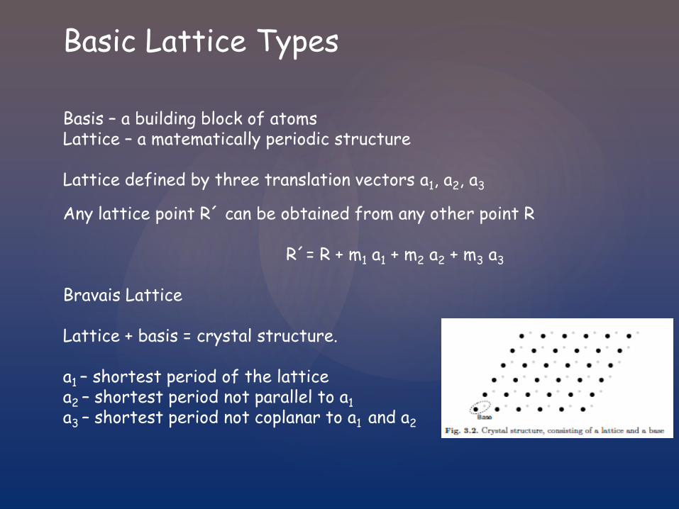
Basic Lattice Types
Basis – a building block of atoms Lattice – a matematically periodic structure Lattice defined by three translation vectors a1, a2, a3 Any lattice point R´ can be obtained from any other point R
R´= R + m1 a1 + m2 a2 + m3 a3 Bravais Lattice Lattice + basis = crystal structure. a1 – shortest period of the lattice a2 – shortest period not parallel to a1 a3 – shortest period not coplanar to a1 and a2
Basic Lattice Types
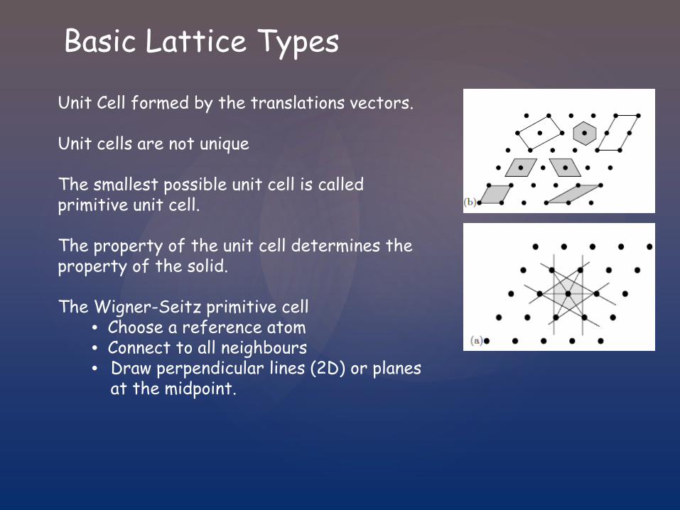
Unit Cell formed by the translations vectors. Unit cells are not unique The smallest possible unit cell is called primitive unit cell. The property of the unit cell determines the property of the solid. The Wigner-Seitz primitive cell
• Choose a reference atom • Connect to all neighbours • Draw perpendicular lines (2D) or planes
at the midpoint.
Basic Lattice Types
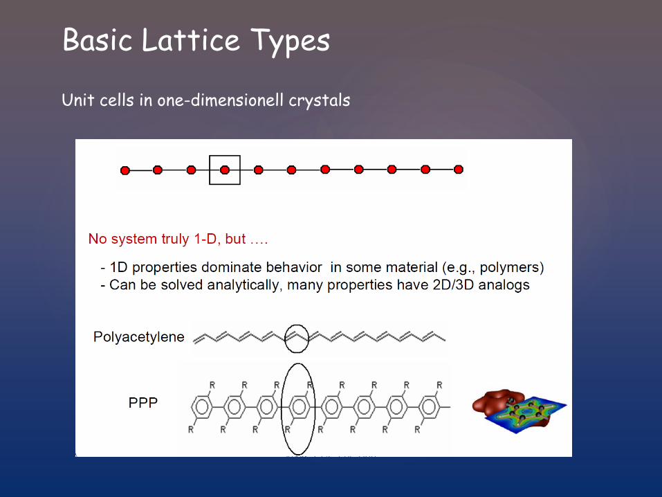
Unit cells in one-dimensionell crystals
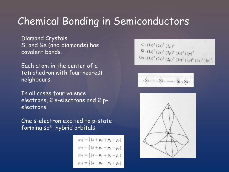
Chemical Bonding in Semiconductors Diamond Crystals Si and Ge (and diamonds) has covalent bonds. Each atom in the center of a tetrahedron with four nearest neighbours. In all cases four valence electrons, 2 s-electrons and 2 p-electrons. One s-electron excited to p-state forming sp3 hybrid orbitals

Basic Lattice Types
14 3D Bravais Lattices sc – simple cubic bcc – body centered cubic fcc – face centered cubic
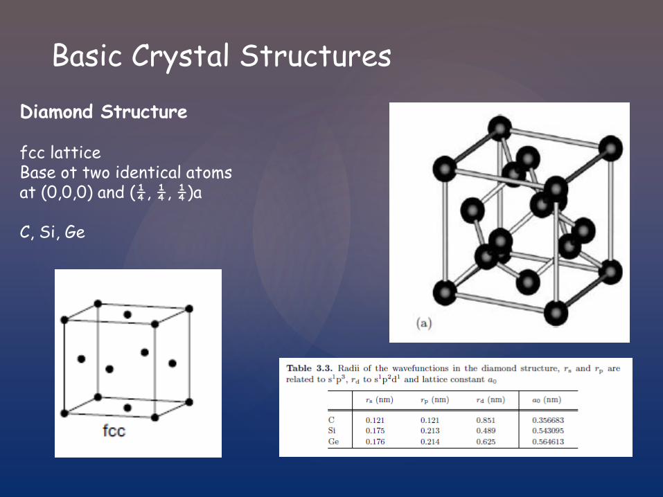
Basic Crystal Structures
Diamond Structure fcc lattice Base ot two identical atoms at (0,0,0) and (¼, ¼, ¼)a C, Si, Ge
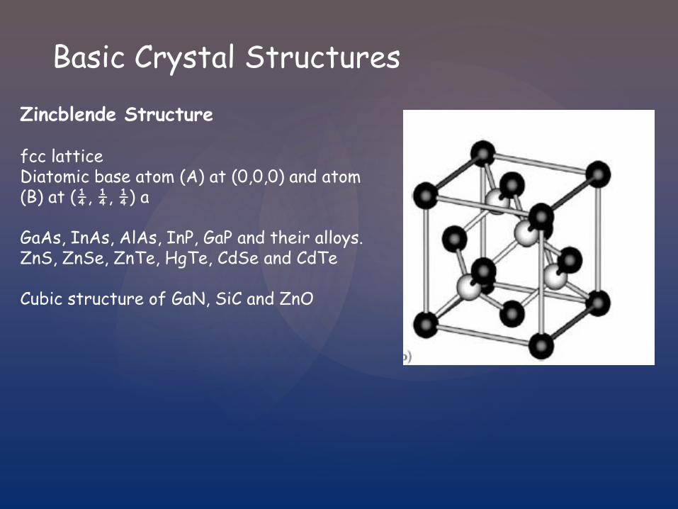
Basic Crystal Structures
Zincblende Structure fcc lattice Diatomic base atom (A) at (0,0,0) and atom (B) at (¼, ¼, ¼) a GaAs, InAs, AlAs, InP, GaP and their alloys. ZnS, ZnSe, ZnTe, HgTe, CdSe and CdTe Cubic structure of GaN, SiC and ZnO

Basic Crystal Structures Wurtzite Structure (Aka hexagonal ZnS) hcp lattice with diatomic base Many semiconductors with high bandgap GaN, AlN, InN, ZnO, SiC, ZnS CdS and CdSe

Basic Crystal Structures
Chalcopyrite Structure (CuFeS2) Tetrahedral structure with triatom base. I-III-VI2 (Mg, Zn, Cd) (S, Ge, Sn) (As, P, Sb) 2
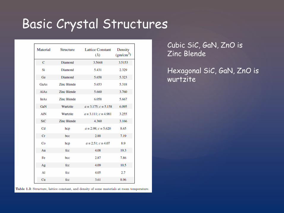
Basic Crystal Structures Cubic SiC, GaN, ZnO is Zinc Blende Hexagonal SiC, GaN, ZnO is wurtzite

Polytypism Stacking sequence not only hcp or fcc But takes different sequences. SiC typical example Each hexagonal atomic layer have three different possible relative positions A, B, and C 3C-SiC : ABC ABC … 4H-SiC : ABCB ABCB … 6H-SiC : ABCACB ABCACB … A Polytypes is a large number of repetition of the same stacking sequence About 45 different observed in SiC Theoretically > 200 Every polytype has different electrical and optical properties
Reciprocal Lattice Reciprocal lattice is important to understand and to study the periodic structure of a crystal.
• X-ray diffraction • phonons • band structure
It is a quasi-Fourier transformation of the direct lattice. R are translations vectors for the direct lattice. G are the corresponding reciprocal lattice vectors. exp( iGR ) = 1 Therefore, for all vectors r and the reciprocal lattice vector G exp( iG(r+R) ) = exp( iGr ) Each Bravais lattice has a certain reciprocal lattice, which also is a Bravais lattice.

Reciprocal Lattice
Reciprocal lattice vectors
b1 = 2π ( a2 x a3) / Va b2 = 2π ( a3 x a1 ) / Va Va = a1 ( a2 x a3 ) volume of unit cell b3 = 2π ( a1 x a2 ) / Va
Any arbitrary set of primitive vectors a1, a2 and a3 of a given crystal lattice gives a set of reciprocal lattice points. G = h b1 + k b2 + l b3 h,k,l are integers Every crystal has two lattices, one direct and one reciprocal. The reciprocal of the reciprocal lattice is again the direct lattice. The reciprocal of a bcc is the fcc, and vice versa. The reciprocal lattice of the Wigner-Zeits unit cell is called Brillouin zone

Brilloun Zone
For fcc
fcc
hcp
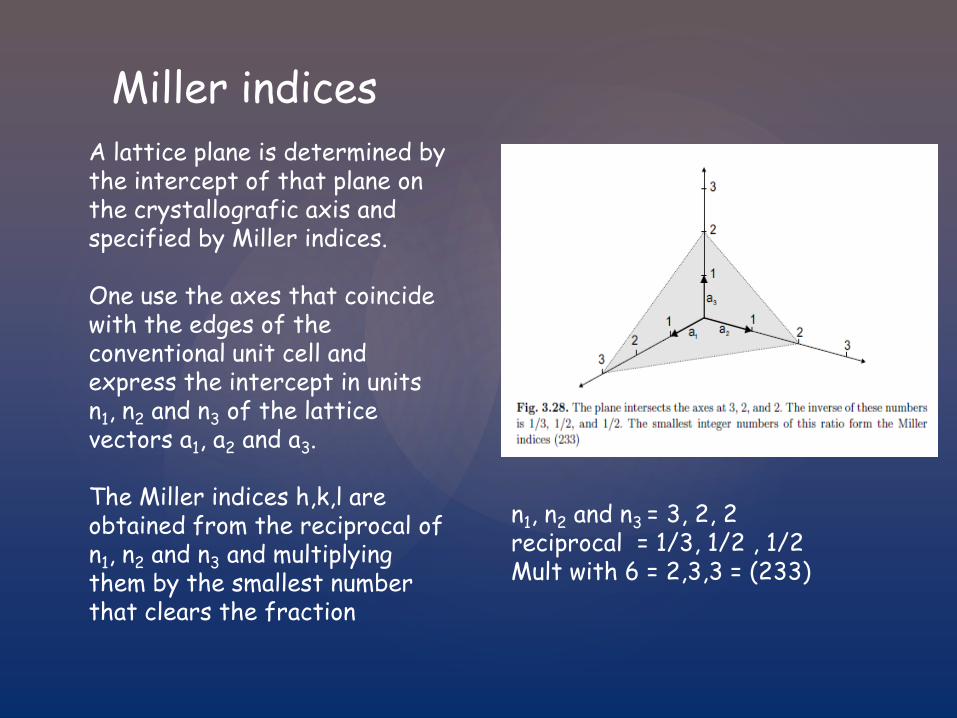
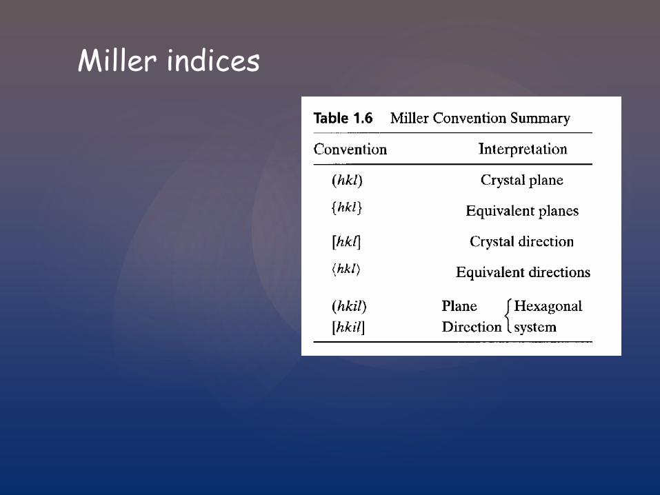
Miller indices
A lattice plane is determined by the intercept of that plane on the crystallografic axis and specified by Miller indices. One use the axes that coincide with the edges of the conventional unit cell and express the intercept in units n1, n2 and n3 of the lattice vectors a1, a2 and a3. The Miller indices h,k,l are obtained from the reciprocal of n1, n2 and n3 and multiplying them by the smallest number that clears the fraction
n1, n2 and n3 = 3, 2, 2 reciprocal = 1/3, 1/2 , 1/2 Mult with 6 = 2,3,3 = (233)

Miller indices Cubic crystals
a1
a2
a3
Miller indices

Miller indices
Hexagonal Lattice In hexagonal lattice four indices (hkil). i = -(h+k) (110) = (11-20)
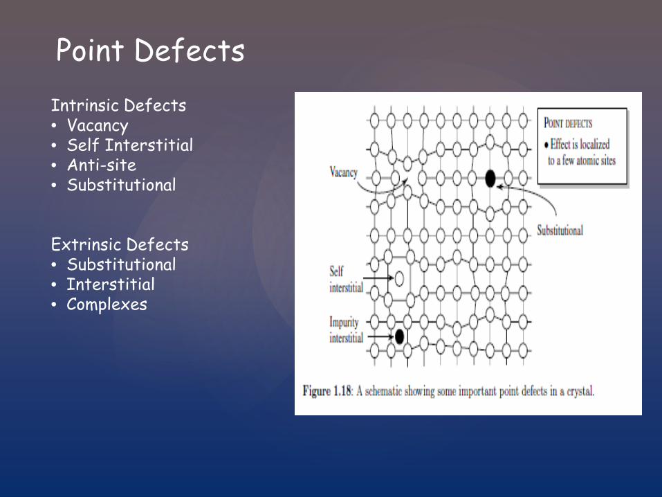
Point Defects Intrinsic Defects • Vacancy • Self Interstitial • Anti-site • Substitutional Extrinsic Defects • Substitutional • Interstitial • Complexes
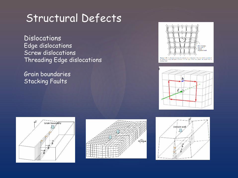
Structural Defects
Dislocations Edge dislocations Screw dislocations Threading Edge dislocations Grain boundaries Stacking Faults
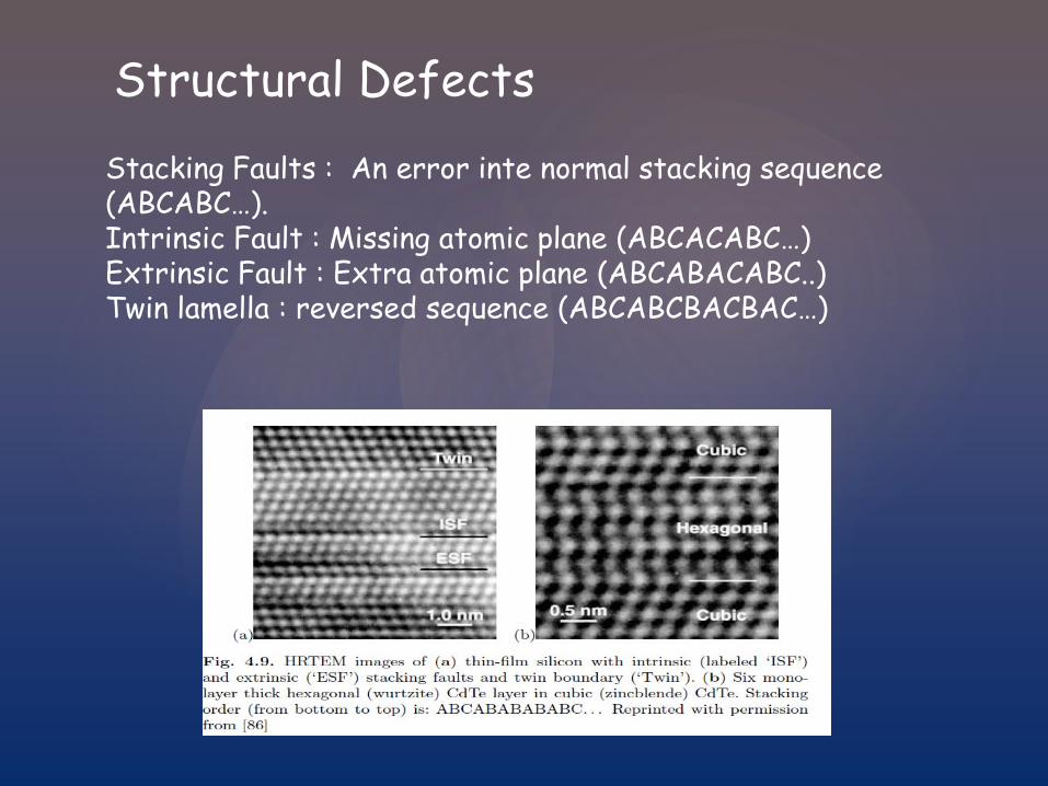
Structural Defects
Stacking Faults : An error inte normal stacking sequence (ABCABC…). Intrinsic Fault : Missing atomic plane (ABCACABC…) Extrinsic Fault : Extra atomic plane (ABCABACABC..) Twin lamella : reversed sequence (ABCABCBACBAC…)

Structural Defects Xray Topography Synchrotron White Beam Xray Topography SWBXT
Reflection Transmission

Structural Defects
Dislocation densities Si 0 – 100 cm-2
SiC 102 – 105 cm-2
GaN 107 cm-2

Polycrystalline Semiconductors
Randomly oriented crystal grains. Used in : Cheap, large area applications.
• Solar cells • Thin film transistors
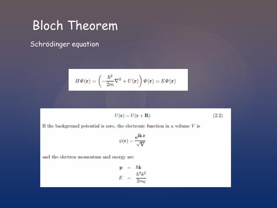
Bloch Theorem Schrödinger equation
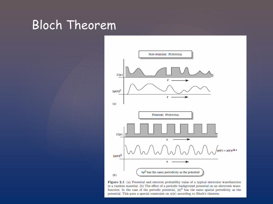
Bloch Theorem
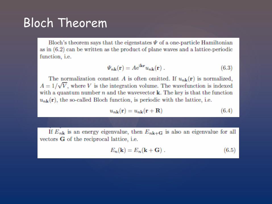
Bloch Theorem

Empty Lattice U(r) = 0
One-dimensional Reduced zone
scc

Kronig Penney Model
Schrödinger Equation En-dimensionell periodic potential Bloch’s teorem Uo ⇒ ∞ b ⇒ 0
Well Barrier
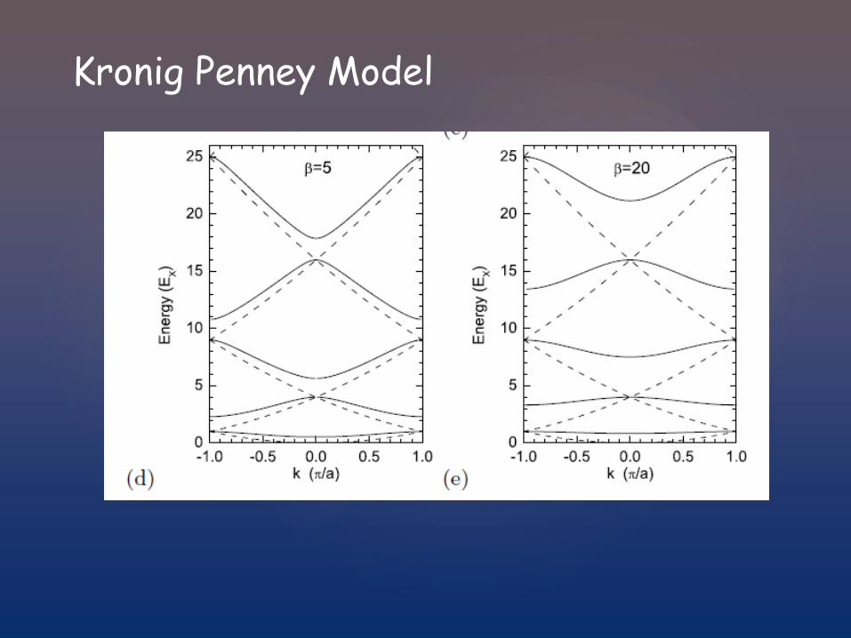
Kronig Penney Model
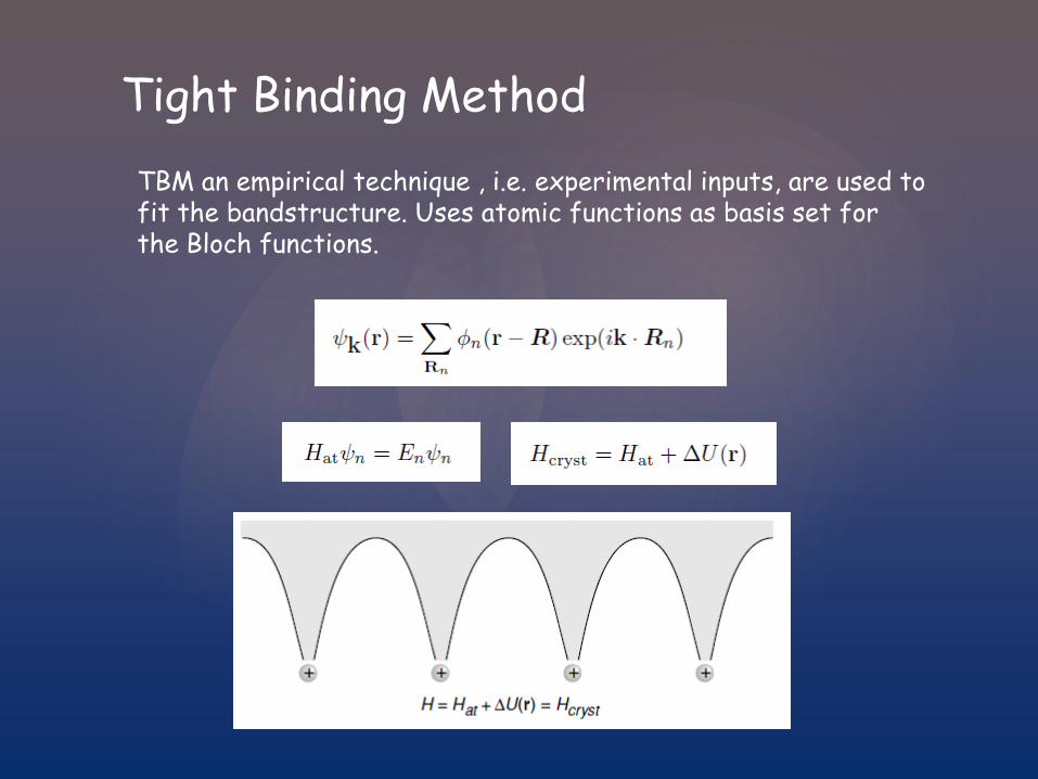
Tight Binding Method TBM an empirical technique , i.e. experimental inputs, are used to fit the bandstructure. Uses atomic functions as basis set for the Bloch functions.
Tight Binding Method
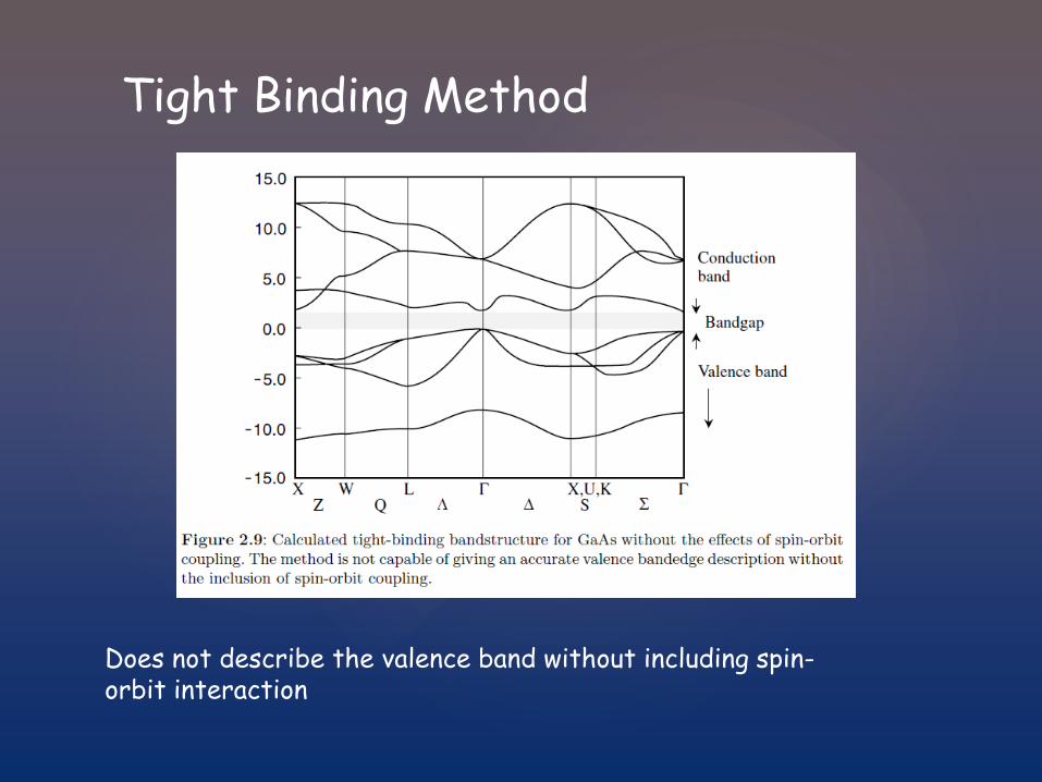
Does not describe the valence band without including spin-orbit interaction

Spin-Orbit Coupling
S : Spin angular momentum L : Orbital angular momentum J : Total angular momentum
Most semiconductor has similar valence bandedge. Without s-o coupling 6-fold degenerate.
S-O coupling 4-fold degenerate 2 HH Heavy Hole 2 LH Light Hole 2 split-off bands
Other Methods
Ortogonalized Plane Wave (OPW) Uses the valence and conduction band states ortogonal to the core states. Simplifies calculations and reduces number plane wave states. Pseudopotential Method The background periodic potential is replace by a new ”pseudopotential” , subtracting the ”core” contribution and constant background perturbation potential. k•p Method Accurate close to bandedges. Used also for low dimensional structures. Starts at bandedges and uses perturbation theory to describe the bands away from high symmetri points.
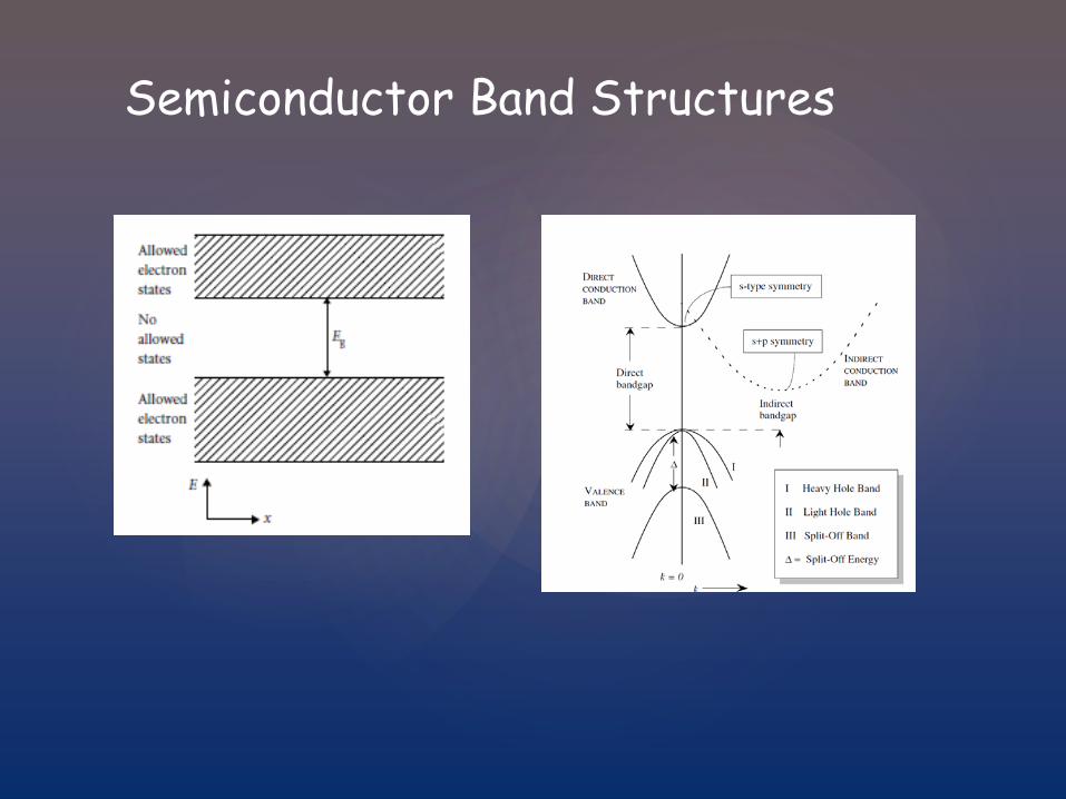
Semiconductor Band Structures
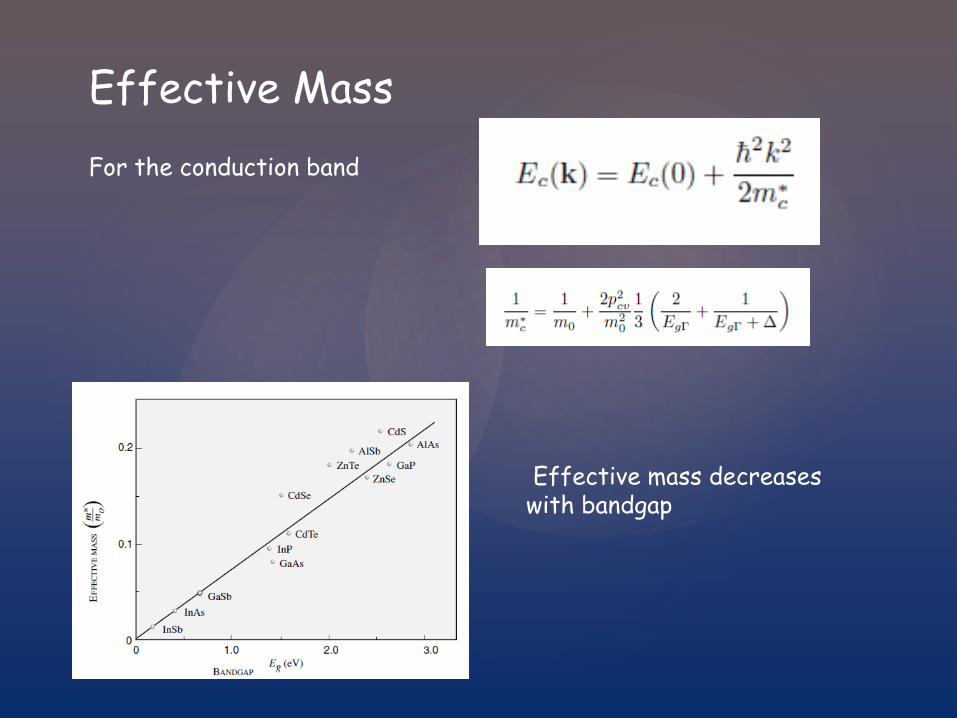
Effective Mass For the conduction band
Effective mass decreases with bandgap
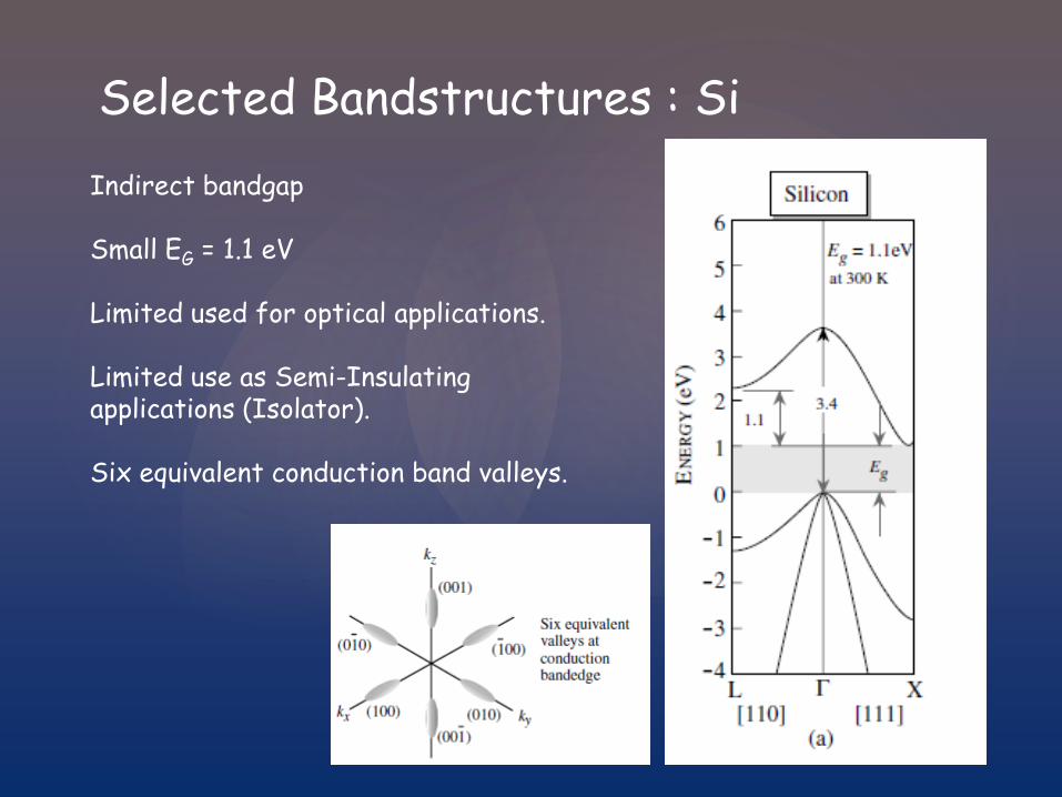
Selected Bandstructures : Si Indirect bandgap Small EG = 1.1 eV Limited used for optical applications. Limited use as Semi-Insulating applications (Isolator). Six equivalent conduction band valleys.
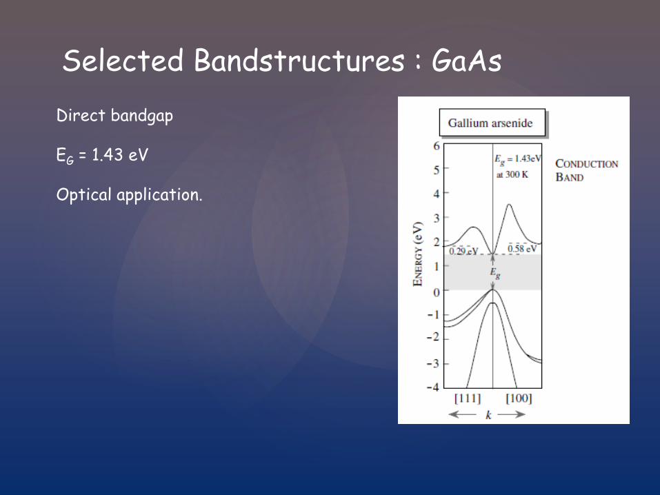
Selected Bandstructures : GaAs Direct bandgap EG = 1.43 eV Optical application.
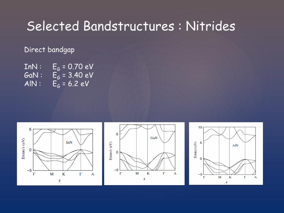
Selected Bandstructures : Nitrides Direct bandgap InN : EG = 0.70 eV GaN : EG = 3.40 eV AlN : EG = 6.2 eV
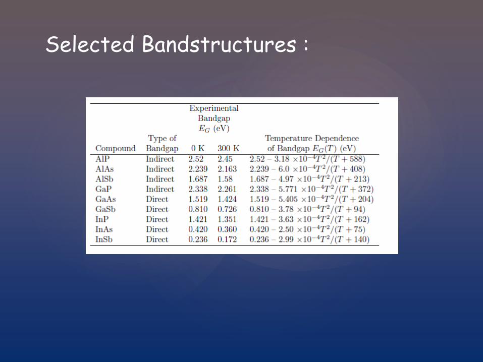
Selected Bandstructures :