Area 1: Semiconductor Physics · Area 1: Semiconductor Physics ... Learn basics of semiconductor...
13
(1) Area 1: Semiconductor Physics Sorin P. Voinigescu
Transcript of Area 1: Semiconductor Physics · Area 1: Semiconductor Physics ... Learn basics of semiconductor...
(1)
Area 1: Semiconductor Physics
Sorin P. Voinigescu
(2)
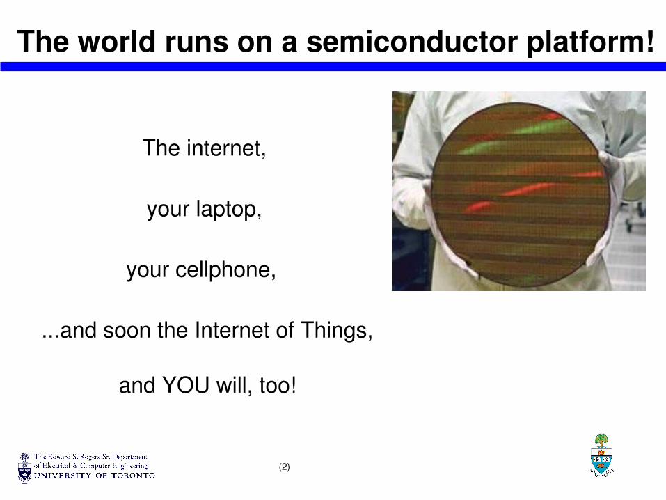
The world runs on a semiconductor platform!
The internet,
your laptop,
your cellphone,
...and soon the Internet of Things,
and YOU will, too!
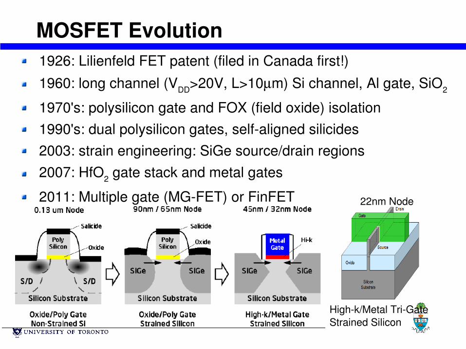
MOSFET Evolution1926: Lilienfeld FET patent (filed in Canada first!)
1960: long channel (VDD>20V, L>10m) Si channel, Al gate, SiO2
1970's: polysilicon gate and FOX (field oxide) isolation1990's: dual polysilicon gates, selfaligned silicides2003: strain engineering: SiGe source/drain regions2007: HfO2 gate stack and metal gates
2011: Multiple gate (MGFET) or FinFET 22nm Node
Highk/Metal TriGateStrained Silicon
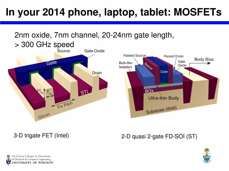
In your 2014 phone, laptop, tablet: MOSFETs
3D trigate FET (Intel) 2D quasi 2gate FDSOI (ST)
2nm oxide, 7nm channel, 2024nm gate length, > 300 GHz speed
(5)
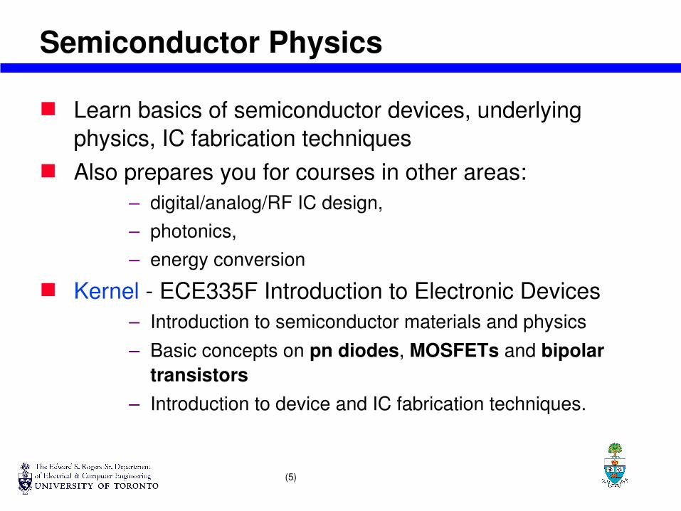
Semiconductor Physics
Learn basics of semiconductor devices, underlying physics, IC fabrication techniques
Also prepares you for courses in other areas:– digital/analog/RF IC design, – photonics, – energy conversion
Kernel ECE335F Introduction to Electronic Devices– Introduction to semiconductor materials and physics– Basic concepts on pn diodes, MOSFETs and bipolar
transistors– Introduction to device and IC fabrication techniques.
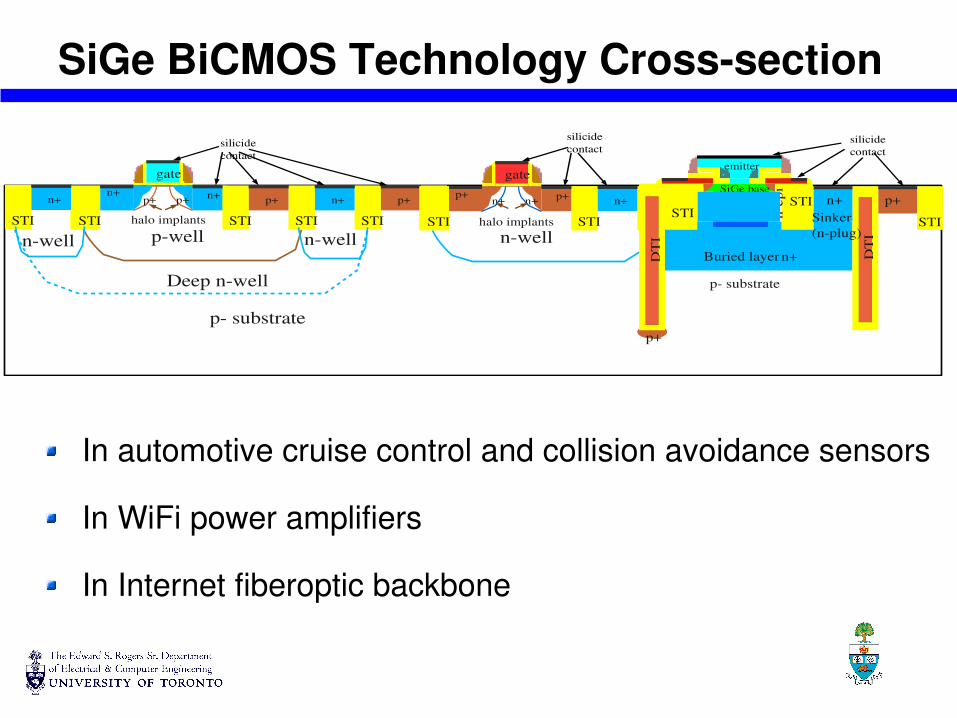
SiGe BiCMOS Technology Crosssection
p+
STI STIpwell
gate
p+ p+
halo implants
n+ n+
STI
p+
STI
n+
Deep nwell
p substrate
STI
p+
silicidecontact
STI STInwell
gate
n+ n+
halo implants
p+ p+
STI
n+
silicidecontact
p+
p+
STI
n+
STI
n+
p substrate
p+
DT
I
DT
I
STI
Buried layer
Sinker(nplug)
nep
i
nep
i
SIC
emitter
SiGe base
silicidecontact
STI
n+
nwellnwell
In automotive cruise control and collision avoidance sensors
In WiFi power amplifiers
In Internet fiberoptic backbone
(7)
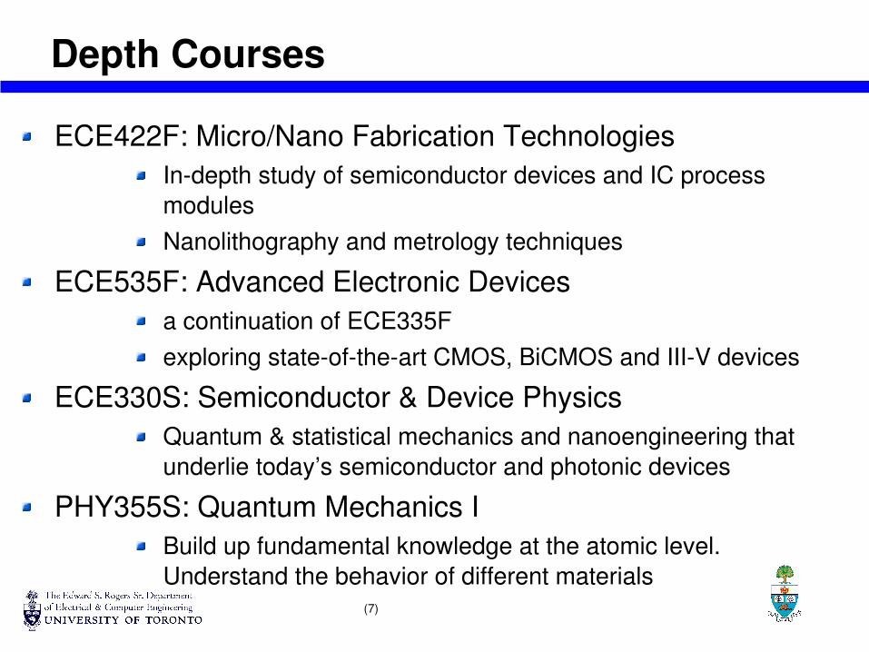
Depth Courses
ECE422F: Micro/Nano Fabrication TechnologiesIndepth study of semiconductor devices and IC process modulesNanolithography and metrology techniques
ECE535F: Advanced Electronic Devicesa continuation of ECE335Fexploring stateoftheart CMOS, BiCMOS and IIIV devices
ECE330S: Semiconductor & Device PhysicsQuantum & statistical mechanics and nanoengineering that underlie today’s semiconductor and photonic devices
PHY355S: Quantum Mechanics IBuild up fundamental knowledge at the atomic level. Understand the behavior of different materials
8
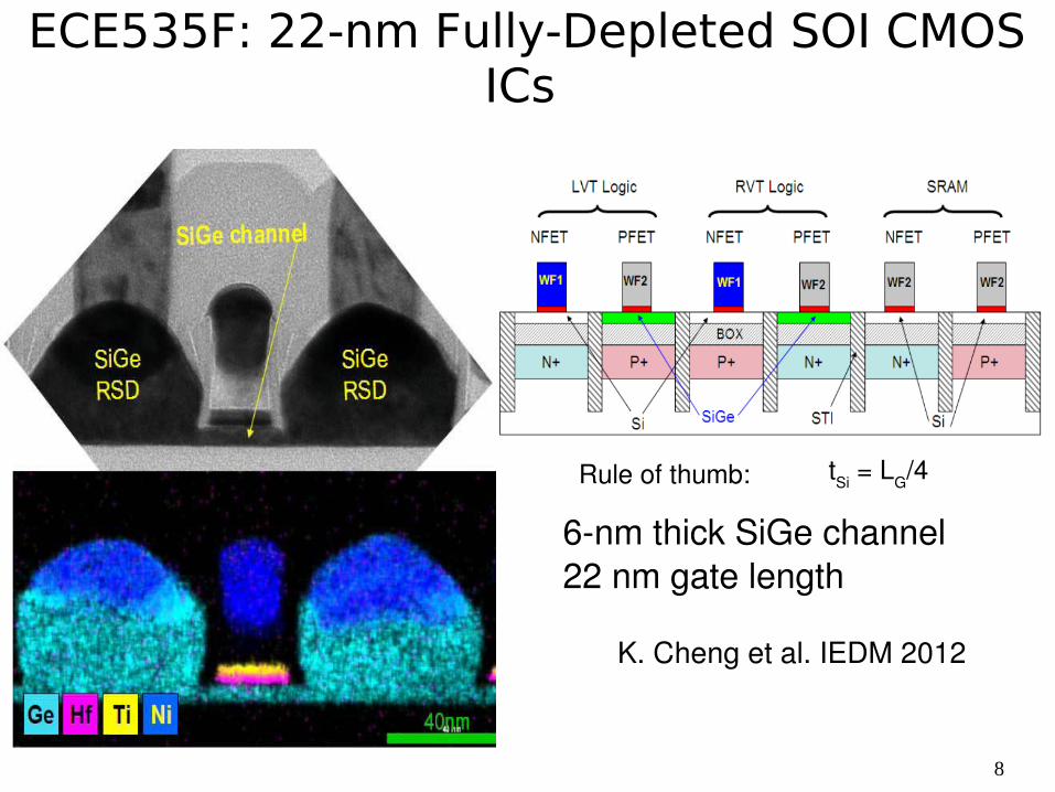
K. Cheng et al. IEDM 2012
ECE535F: 22-nm Fully-Depleted SOI CMOS ICs
6nm thick SiGe channel22 nm gate length
tSi = LG/4Rule of thumb:
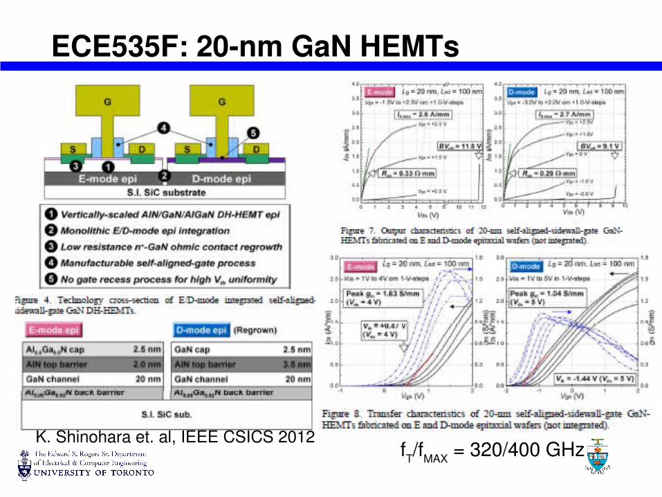
ECE535F: 20nm GaN HEMTs
K. Shinohara et. al, IEEE CSICS 2012fT/fMAX = 320/400 GHz
(10)
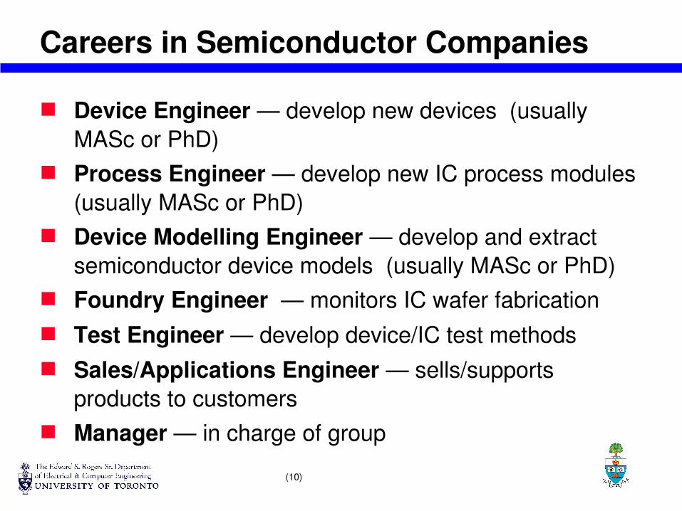
Careers in Semiconductor Companies
Device Engineer — develop new devices (usually MASc or PhD)
Process Engineer — develop new IC process modules (usually MASc or PhD)
Device Modelling Engineer — develop and extract semiconductor device models (usually MASc or PhD)
Foundry Engineer — monitors IC wafer fabrication Test Engineer — develop device/IC test methods Sales/Applications Engineer — sells/supports
products to customers Manager — in charge of group
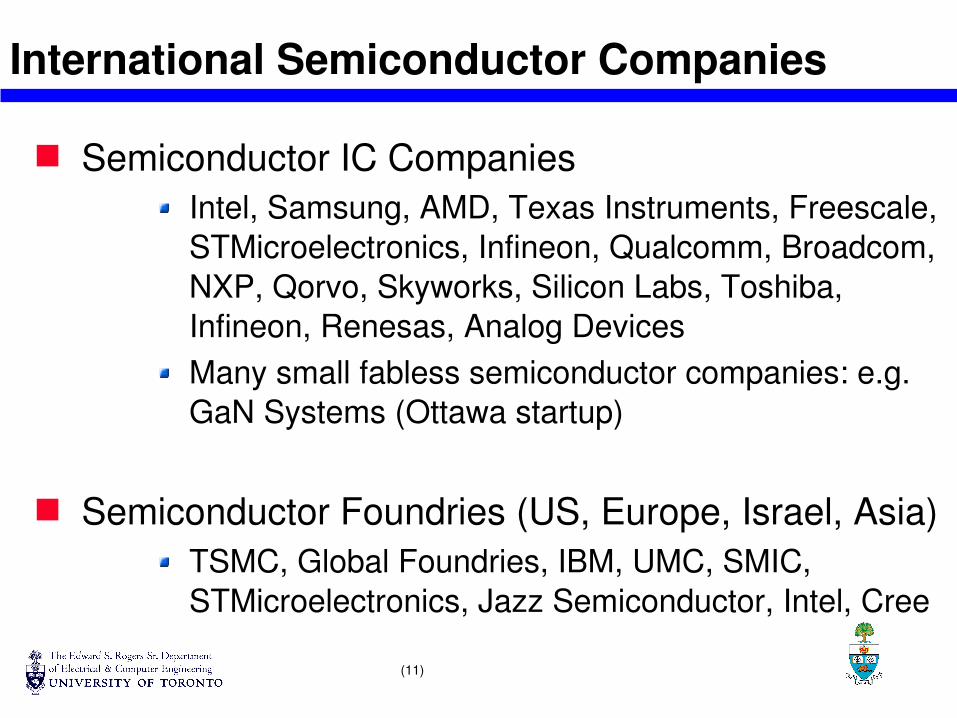
(11)
International Semiconductor Companies
Semiconductor IC CompaniesIntel, Samsung, AMD, Texas Instruments, Freescale, STMicroelectronics, Infineon, Qualcomm, Broadcom, NXP, Qorvo, Skyworks, Silicon Labs, Toshiba, Infineon, Renesas, Analog DevicesMany small fabless semiconductor companies: e.g. GaN Systems (Ottawa startup)
Semiconductor Foundries (US, Europe, Israel, Asia)TSMC, Global Foundries, IBM, UMC, SMIC, STMicroelectronics, Jazz Semiconductor, Intel, Cree
Semiconductor Industry

Questions?