SEMICONDUCTOR PHYSICS -
21
SEMICONDUCTOR PHYSICS Introduction: A semiconductor is a material that has a resistivity value in between that of a conductor and an insulator. The conductivity of a semiconductor material can be varied under an external electric field. Devices made from semiconductor materials are the foundation of modern electronics, including ratio, computers , telephones, and may other devices. Semiconductor devices include the transistor, many kinds of diodes including the light emitting diode, the silicon controlled rectifier, and digital and analog integrated circuits. Solar photovoltaic panels are large semiconductor devices that directly convert light energy into electrical energy. In a metallic conductor, current is carried by the flow of electrons. In semiconductors, current can be carried either by the flow of electrons or by the flow of positively charged holes in the electron structure of the material. Silicon is used to create most semiconductors commercially. So many other materials are used, including germanium, gallium arsenide. A pure semiconductor is often called an intrinsic material and then allowing the melt to solidify into a new and different crystal. This process is called doping. Question: Explain the preparation of semi conducting materials? Answer: Preparation of semiconductor materials: Semiconductors with predeictable, reliable electronic properties are necessary for mass production. The level of chemical purity needed is extremely high because the presence of impurities even in very small proportions can have large effects on the properties of material. High degree of crystalline perfection is also required, since faults in crystal structure ( such as dislocations, twins and stacking faults) interfere with the semi- conducting properties of the material. Crystalline faults are a major cause of defective semiconductor devices. The larger the crystal, the more difficult it is to achieve the necessary perfection. Convert mass production processes use crystal ingots between 100 nm and 300 nm (4-12 inches) in a diameter which are grown as cylinders and sliced into wafers. Because of the required level of chemical purity and the perfection of the crystal structure which are needed to make semiconductor devices, special methods have been developed to produce the initial semiconductor material. A technique for achieving high purity includes growing the crystal using the Czocharalski process. As additional step that can be used to further increase purity is known as zone refining. In zone refining , apart of a solid crystal is melted. The impurities tend to concentrate in the melted region, while the desired materials, recrystallizes leaving the solid material more pure and with fewer crystalline faults. In manufacturing semiconductor devices involving hetero-junctions between different semiconductor materials, the lattice constant, which is the length of the repeating elements of the crystal structure, is important for determining the compatibility of material. Question : Define conduction band and valence band ? Answer: Conduction band: The conduction band in the range of electron energy, higher than that of the valence band, sufficient to make the electrons free to accelerate under the influence of an applied electric field and thus constitutes an electric current. Semiconductors may cross this conduction band when they are excited. Valence band:
Transcript of SEMICONDUCTOR PHYSICS -
SEMICONDUCTOR PHYSICS
Introduction:
A semiconductor is a material that has a resistivity value in between that of a conductor and an insulator.The conductivity of a semiconductor material can be varied under an external electric field. Devices madefrom semiconductor materials are the foundation of modern electronics, including ratio, computers ,telephones, and may other devices. Semiconductor devices include the transistor, many kinds of diodesincluding the light emitting diode, the silicon controlled rectifier, and digital and analog integrated circuits.Solar photovoltaic panels are large semiconductor devices that directly convert light energy into electricalenergy.
In a metallic conductor, current is carried by the flow of electrons. In semiconductors, current can be carriedeither by the flow of electrons or by the flow of positively charged holes in the electron structure of thematerial. Silicon is used to create most semiconductors commercially. So many other materials are used,including germanium, gallium arsenide. A pure semiconductor is often called an intrinsic material and thenallowing the melt to solidify into a new and different crystal. This process is called doping.
Question: Explain the preparation of semi conducting materials?
Answer:
Preparation of semiconductor materials:
Semiconductors with predeictable, reliable electronic properties are necessary for mass production. Thelevel of chemical purity needed is extremely high because the presence of impurities even in very smallproportions can have large effects on the properties of material. High degree of crystalline perfection is alsorequired, since faults in crystal structure ( such as dislocations, twins and stacking faults) interfere with thesemi- conducting properties of the material. Crystalline faults are a major cause of defective semiconductordevices. The larger the crystal, the more difficult it is to achieve the necessary perfection. Convert massproduction processes use crystal ingots between 100 nm and 300 nm (4-12 inches) in a diameter which aregrown as cylinders and sliced into wafers.
Because of the required level of chemical purity and the perfection of the crystal structure which are neededto make semiconductor devices, special methods have been developed to produce the initial semiconductormaterial. A technique for achieving high purity includes growing the crystal using the Czocharalski process.As additional step that can be used to further increase purity is known as zone refining. In zone refining ,apart of a solid crystal is melted. The impurities tend to concentrate in the melted region, while the desiredmaterials, recrystallizes leaving the solid material more pure and with fewer crystalline faults. Inmanufacturing semiconductor devices involving hetero-junctions between different semiconductormaterials, the lattice constant, which is the length of the repeating elements of the crystal structure, isimportant for determining the compatibility of material.
Question : Define conduction band and valence band ?
Answer:
Conduction band:
The conduction band in the range of electron energy, higher than that of the valence band, sufficient to makethe electrons free to accelerate under the influence of an applied electric field and thus constitutes an electriccurrent. Semiconductors may cross this conduction band when they are excited.
Valence band:
The valence band is the highest range of electron energies where electrons are normally present absolutezero. In semiconductors and insulators, there is a band gap above the valence band, followed by conductionband above that. In metals, the conduction band has no energy gap separating it from the valence band .
Semiconductors and insulators owe their high conductivity to the properties of the balance band in thosematerials. It just so happens that the number of electrons is precisely equal to the number of states availableup to the top of the valence band. There are no available states in the band gap. This means that when anelectric field is applied , the electrons can not increase their energy because there are no states available tothe electrons where they would be moving faster than they are already going. There is some conductivity ininsulators, however this is due to thermal excitation of some of the electrons get enough energy to jump theband gap in one go. Once they are in the conduction band, they can conduct electricity, as the hole they leftbehind in the valence band. The hole is an empty state that allows electrons in the valence band somedegree of freedom.
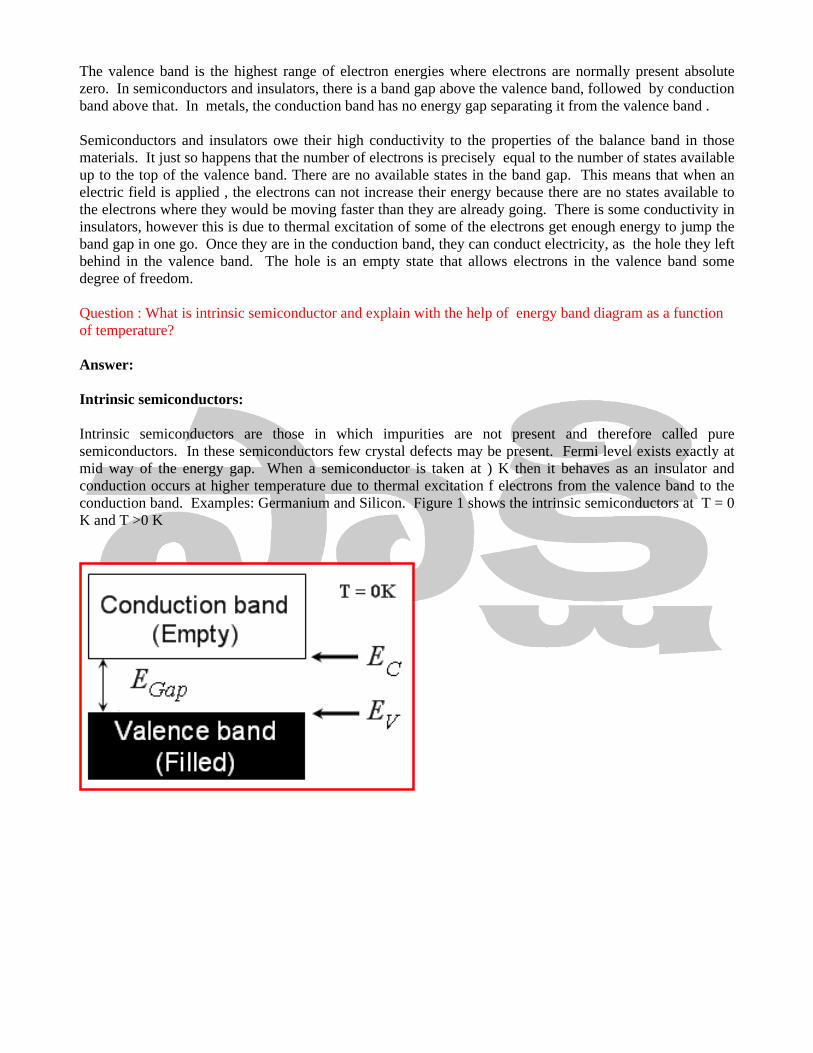
Question : What is intrinsic semiconductor and explain with the help of energy band diagram as a functionof temperature?
Answer:
Intrinsic semiconductors:
Intrinsic semiconductors are those in which impurities are not present and therefore called puresemiconductors. In these semiconductors few crystal defects may be present. Fermi level exists exactly atmid way of the energy gap. When a semiconductor is taken at ) K then it behaves as an insulator andconduction occurs at higher temperature due to thermal excitation f electrons from the valence band to theconduction band. Examples: Germanium and Silicon. Figure 1 shows the intrinsic semiconductors at T = 0K and T >0 K
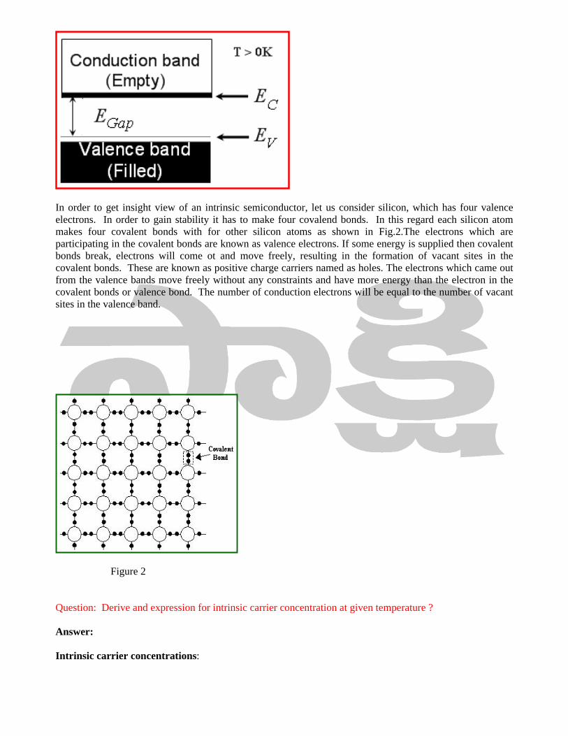
In order to get insight view of an intrinsic semiconductor, let us consider silicon, which has four valenceelectrons. In order to gain stability it has to make four covalend bonds. In this regard each silicon atommakes four covalent bonds with for other silicon atoms as shown in Fig.2.The electrons which areparticipating in the covalent bonds are known as valence electrons. If some energy is supplied then covalentbonds break, electrons will come ot and move freely, resulting in the formation of vacant sites in thecovalent bonds. These are known as positive charge carriers named as holes. The electrons which came outfrom the valence bands move freely without any constraints and have more energy than the electron in thecovalent bonds or valence bond. The number of conduction electrons will be equal to the number of vacantsites in the valence band.
Figure 2
Question: Derive and expression for intrinsic carrier concentration at given temperature ?
Answer:
Intrinsic carrier concentrations:
In intrinsic semidonductors, as the temperature is increased electron-hole pairs will be generated. Hence theelectron concentration, ni, in the conduction band will be equal t the hole concentration, pi in the valenceband.
Let Ei be the Fermi level of the intrinsic semiconductor in equilibrium, then the number of electrons per unitvolume in the conduction band,
−
=TK
EE
h
TKmn
B
ciBei exp
22
2
2
π--------------------(1)
and the number of holes per unit volume in the valence band,
.
−
=TK
EE
h
TKmp
B
ivBhi exp
22
2/3
2
π-----------------(2)
But, in intrinsic semiconductors ni = pi hence,
−
TK
EE
h
TKm
B
ciBe exp2
22/3
2
π=
−
TK
EE
h
TKm
B
ivBh exp2
22/3
2
π
−TK
EEm
B
cie exp2/3 =
−TK
EEm
B
ivh exp2/3
22/3
ln
=−−
e
hByci m
mTKEEE
( )
+−=
e
hvci m
mEEE ln
4
3
2
1
If the effective masses me = mh, then
.2
vci
EEE
+= (since ln1=0) ----------------------(3)
Ei lies midway between Ec and Ev, which happens to be the centre of the band gap any temperature.
If mh>me, Ei linearly increases towards Ec. The material properties Ec, Ev, mh and me determine the value ofEi, which for most semiconductors like Si and Ge lie at the centre of the band gap.
Combining ni and pi, values
2/3
2
24.
=h
KTmpn e
ii
2/3
2
2
h
KTme
−TK
EE ciexp
−TK
EE ivexp
( )
−
=KT
EETmm
h
Kn iv
hei exp2
4 32/33
2 π ( )ii pSincen =
−=KT
EgATn exp32 ---------------- (4)
where
. ( ) 2/33
24 ehmm
h
KA
= π
and Eg = Ec-Ev is the energy gap of the semiconductor.Where A and Eg are constants for a given semiconductor and ni is called the intrinsic concentration whichindicates thermally generated electrons and holes. It is a strong function of temperature T.
Question:
Define Extrinsic semiconductor and how many types of extrinsic semiconductors are available withexamples?
Answer:
Extrinsic semiconductors:
In intrinsic or pure semiconductors, the carrier concentration of both electrons and holes at normaltemperatures very low, hence to get appreciable current density through the semiconductor, a large electricfield should be applied. This problem can overcome by adding suitable impurities into the intrinsicsemiconductors.
The extrinsic semiconductors are those in which impurities of large quantity are present. In general, theimpurities can be either III group elements or V group elements. Based on the impurities present in theextrinsic semiconductors, they are classifies into two categories.
1. n-type semiconductors and2. p-type semiconductors
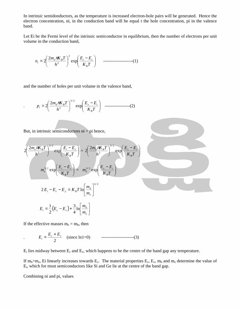
n-type semiconductors:
In order for silicon crystal to conduct electricity, we need to introduce an impurity atom such as Arsenic,Antimony or phosphorus into the crystalline structure. These atoms have five outer electrons in theiroutermost co-valent bond to share with other atoms and are commonly called pentavalent impurities. Thisallows four of the five electrons tobond with its neighboring silicon atoms leaving one free electron to moveabout when electrical voltage is applied. As each impurity atom donates one electron, pentavalent atoms aregenerally known as donors. Antimoney (Sb) is frequently used as pentavalent additive as it has 51 electronsarranged in 5 shells around the nucleus. The resulting semiconductor material has an excess of currentcarrying electrons, each with a negative charge, and is therefore referred to as n-type material with the
electrons called majority carriers and the resultant holes minority carriers. The block diagram of n-typeimpurity doping and corresponding band diagram is shown in figure 1.
\
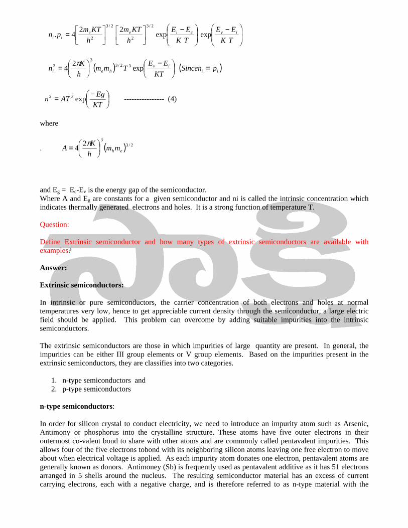
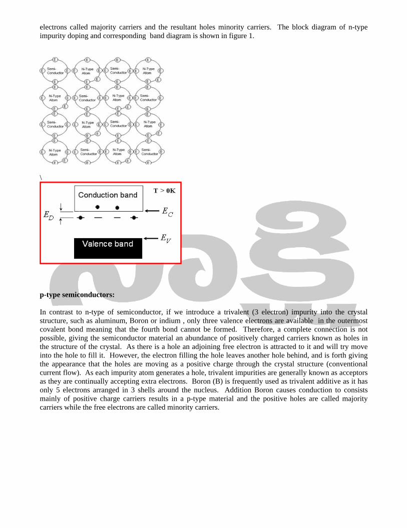
p-type semiconductors:
In contrast to n-type of semiconductor, if we introduce a trivalent (3 electron) impurity into the crystalstructure, such as aluminum, Boron or indium , only three valence electrons are available in the outermostcovalent bond meaning that the fourth bond cannot be formed. Therefore, a complete connection is notpossible, giving the semiconductor material an abundance of positively charged carriers known as holes inthe structure of the crystal. As there is a hole an adjoining free electron is attracted to it and will try moveinto the hole to fill it. However, the electron filling the hole leaves another hole behind, and is forth givingthe appearance that the holes are moving as a positive charge through the crystal structure (conventionalcurrent flow). As each impurity atom generates a hole, trivalent impurities are generally known as acceptorsas they are continually accepting extra electrons. Boron (B) is frequently used as trivalent additive as it hasonly 5 electrons arranged in 3 shells around the nucleus. Addition Boron causes conduction to consistsmainly of positive charge carriers results in a p-type material and the positive holes are called majoritycarriers while the free electrons are called minority carriers.
Question: Estimate electron and hole densities?
Answer:
Electron and hole Densities:
The computation of the elecgtron and hole densities in semi-conductor is the most important application ofFermi-Dirac statists.
Carrier density at a given level in n-type semiconductor:
Consider an extrinsic semiconductor doped with donor atoms give rise to donor levels E d close to theconduction band edge Ec as shown in Fig. Let Nd be the number of impurity of atoms, gives rise to a singleelectron state at Ed. Then the number of electrons in the energy level Ed would be
)()( deded EPEgN = --------------------(1)
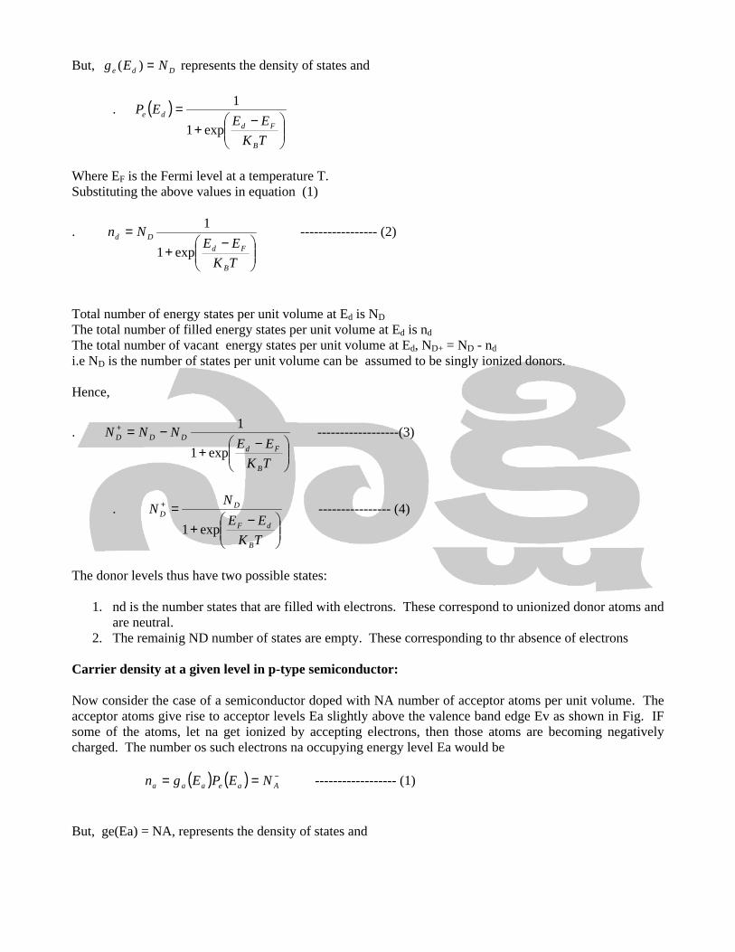
But, Dde NEg =)( represents the density of states and
. ( )
−+
=
TK
EEEP
B
Fd
de
exp1
1
Where EF is the Fermi level at a temperature T.Substituting the above values in equation (1)
.
−+
=
TK
EENn
B
Fd
Dd
exp1
1----------------- (2)
Total number of energy states per unit volume at Ed is ND
The total number of filled energy states per unit volume at Ed is nd
The total number of vacant energy states per unit volume at Ed, ND+ = ND - nd
i.e ND is the number of states per unit volume can be assumed to be singly ionized donors.
Hence,
.
−+
−=+
TK
EENNN
B
Fd
DDD
exp1
1------------------(3)
.
−+
=+
TK
EE
NN
B
dF
DD
exp1
---------------- (4)
The donor levels thus have two possible states:
1. nd is the number states that are filled with electrons. These correspond to unionized donor atoms andare neutral.
2. The remainig ND number of states are empty. These corresponding to thr absence of electrons
Carrier density at a given level in p-type semiconductor:
Now consider the case of a semiconductor doped with NA number of acceptor atoms per unit volume. Theacceptor atoms give rise to acceptor levels Ea slightly above the valence band edge Ev as shown in Fig. IFsome of the atoms, let na get ionized by accepting electrons, then those atoms are becoming negativelycharged. The number os such electrons na occupying energy level Ea would be
( ) ( ) −== Aaeaaa NEPEgn ------------------ (1)
But, ge(Ea) = NA, represents the density of states and
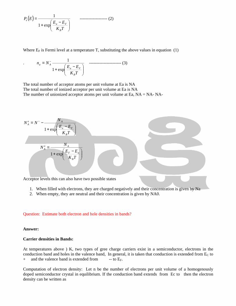
( ) =EPe
−+
TK
EE
B
Faexp1
1------------------- (2)
Where EF is Fermi level at a temperature T, substituting the above values in equation (1)
.
−+
= −
TK
EENn
B
Fa
Aa
exp1
1---------------------- (3)
The total number of acceptor atoms per unit volume at Ea is NAThe total number of ionized acceptor per unit volume at Ea is NAThe number of unionized acceptor atoms per unit volume at Ea, NA = NA- NA-
−+
−= −
TK
EE
NNN
B
Fa
AoA
exp1
−+
=
TK
EE
NN
B
aF
AoA
exp1
Acceptor levels this can also have two possible states
1. When filled with electrons, they are charged negatively and their concentration is given by Na2. When empty, they are neutral and their concentration is given by NA0.
Question: Estimate both electron and hole densities in bands?
Answer:
Carrier densities in Bands:
At temperatures above ) K, two types of gree charge carriers exist in a semiconductor, electrons in theconduction band and holes in the valence band, In general, it is taken that conduction is extended from EC to+ and the valence band is extended from -- to EF.
Computation of electron density: Let n be the number of electrons per unit volume of a homogenouslydoped semiconductor crystal in equilibrium. If the conduction band extends from Ec to then the electrondensity can be written as
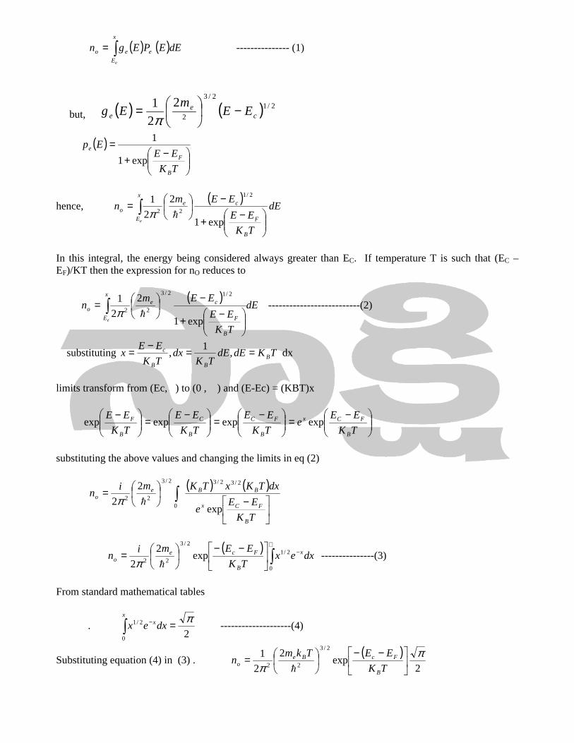
( ) ( )dEEPEgnx
E
eeo
e
∫= --------------- (1)
but, ( ) ( ) 2/12/3
2
2
2
1c
ee EE
mEg −
=π
( )
−+
=
TK
EEEp
B
F
e
exp1
1
hence,( )
∫
−+
−
=x
E
B
F
ceo
e
TK
EE
EEmn
exp1
2
2
1 2/1
22�π
dE
In this integral, the energy being considered always greater than EC. If temperature T is such that (EC –EF)/KT then the expression for nO reduces to
( )dE
TK
EE
EEmn
x
E
B
F
ceo
e
∫
−+
−
=exp1
2
2
1 2/12/3
22�π
--------------------------(2)
substituting TKdEdETK
dxTK
EEx B
BB
c ==−
= ,1
, dx
limits transform from (Ec, ) to (0 , ) and (E-Ec) = (KBT)x
−=
−=
−=
−TK
EEe
TK
EE
TK
EE
TK
EE
B
FCx
B
FC
B
C
B
F expexpexpexp
substituting the above values and changing the limits in eq (2)
( ) ( )
−
= ∫
TK
EEe
dxTKxTKmin
B
FCx
BBeo
exp
2
2
2/32/3
0
2/3
22�π
( )∫∝
−
−−
=0
2/1
2/3
22exp
2
2dxex
TK
EEmin x
B
Fceo
�π---------------(3)
From standard mathematical tables
. ∫ =−x
xdxex0
2/1
2
π--------------------(4)
Substituting equation (4) in (3) .( )
2exp
2
2
12/3
22
ππ
−−
=TK
EETkmn
B
FcBeo
�
( )
−−
=TK
EETkmn
B
FcBeo exp
2
4
12/3
22π
π �
i.e( )
−−
=TK
EETkmn
B
FcBeo exp
2
4
12/3
2π�
( )
−−
=TK
EE
h
Tkm
B
FcBe exp2
4
82/3
2
π
( )
−−
=TK
EE
h
Tkmn
B
FcBeo exp
22
2/3
2
( )
−−=
TK
EENn
B
Fcoo exp ---------------(5)
where2/3
2
22
=h
KTmN e
c
π--------------(6)
Which is called the effective electron density in the conduction band.
Computation of hole density:
Let p be the number of holes per unit volume of a homogenously doped semiconductor crystal inequilibrium. If the valence band extends from - to EV, the hole density, P0 in a homogenous dopedsemiconductors can be written as
. dEEpEgp hh
E
x
o )()(∫−
= ------------------- (1)
But, ( )
−+
=−
=
TK
EEEPEE
mEg
B
F
hvh
h
exp1
1)(,
2
2
1)( 2/1
2/3
22�π
Hence, .( )
dE
TK
EE
EEmp
vE
x
B
F
vho ∫
−
−+
−⋅
=exp1
2
2
1 2/12/3
22�π
In this integral, the energy E being considered always lesser than EV. If the temperature is such that EF –EV5KBT
( ) dEEETK
EEmp v
E
x B
Fho
v2/1
2/3
22exp
2
2
1 −
−
= ∫− �π
------------------- (2)
Substituting,
TK
dEdxx
TK
EE
BB
v −==−
, dE = -KBTdx
limits transform from [ EF- ]
exp( ) ( ) ( )
−
−−=
−TK
EE
TK
EE
TK
EE
B
Fv
B
Fv
B
F expexp
Substituting the above values and changing the limits in equation (2)
. ( ) ( ) dETK
EEdxeTKx
mp
B
FvxE
x
x
Bh
o
v
−−−
= −
−∫ ∫ exp
2
2
12/3
0
2/12/3
22�π
dxexTK
EETKmp
xx
B
FvBho ∫
−
−
=0
2/122
exp2
2
1
�π-------------- (3)
from standard integrals
. ∫ =−x
xdxex0
2/1
2
π
Substituting equation eq (3) in eq(2)
−
=TK
EE
h
TKmp
B
FvBho exp
22
2
π
−=
TK
EENp
B
Fvvo exp --------------- (4)
Where2/3
2
22
=h
TKmN Bh
v
π------------------ (5)
Question: Define drift current and obtain an expression for conductivity?
Answer: Drift current and conductivity:
In the presence of electric field, the drift velocity dhde VV & of carriers superpose on the thermal velocities
thte VV & . But the flow of charge carriers result in an electric currents in the semiconductor crystal known
as the drift currents. Let an electric field E be applied in the positive X-direction creating drift currents
pdnd JJ & of electrons and holes respectively.
When electric field is removed , the carriers moving with a uniform velocity in the negative X-direction dueto the application of electric field E in the positive X-direction. Suppose AB, a small rectangular boxelement of length and unit sides of the square end faces a and B in the semiconductor as shown in Fig.1
{ } { }
××=
Particleseach
onChargeParticlesofDensityParticlesofDensity
ABboxthe
inchargeTotalQ
( ) qnQ de −××××= 11υ
Thus, qQ −= n dev ------------------(1)
Where n is the number of electrons per unit volume. The entering charge into the box through the face Awill cross the face B in unit time. Thus, the drift current density J due to the free electrons at the face B willbe
J=Areatime
ech
×arg
----------------------(2)
From eq (1) and (2), the current density of electrons,
qJ nd −= n dev
similarly the current density of holes,qJ pd = p dhv ------------------ (3)
But, the drift velocities in terms of mobilities are−=dev nµ E -------------(4)
=dhv pµ E -------------(5)
Hence, substituting equations eq (4) and (5) in equation (2)
nJ nd = q nm E
AndpqJ pd = pµ E
Even though electrons and holes move in opposite direction, the effective charge flow is same for both andhence they get added up. Hence the total current density die to both electrons and holes will be
( )EJ
JJJ
d
pdndd
pn pqnq µµ +=
+=----------------------(6)
But, according to Ohm’s law, the current density,
σ=dJ E -----------------------(7)
On comparing the equations (5) and (6), the conductivity
n=σ q pn +µ q pµ
pn σσσ +=
Where nn =σ q nµ and pp =σ q pµ , the electrical conductivities due to electrons and holes
respectively,
In a strong n-type semiconductor n0>>p0, Hence σn >>σp and σ~σn
But, the electric field at a point is, the negative potential gradient, and thus, gradient of any of the energylevels EC, EV or EF, Thus,
x
VE
∂∂−=
dx
E
qE c∂
= 1
dx
E
qv∂
= 1
qE
1=dx
Ei∂
Therefore,
=ndJdx
E
qE in ∂
=σ
dx
E
qcn ∂
=σ
dx
E
qvn ∂
=σ
Question: Give short notes on diffusion currents?
Answer:
Diffusion currents: A directed movement of charge carriers constitute an electric current. Diffusion takesplace die to the existence of a non-uniform concentration of carriers. In fact, Fick’s first law states that thediffusion flux F i.e, the particle current is proportional to and in a direction opposite to the concentrationgradient of the particles. Mathematically it can be written as
Diffusion Currents
x
NF
∂∂−∝
x
NDF
∂∂−= ---------------(1)
Where D is the diffusion constant.
If n and p are the electron and hole concentrations, then the flux densities of electrons and holes Je and Jn canbe written as
x
NDJ ne ∂
∂−= -------------------(2)
x
pDJ ph ∂
∂−= ------------------(3)
Where Dn and Dp are diffusion constants of the electrons and holes respectively,
Then diffusion current densities become,
nJ diff =x
nqDn ∂
∂+
pJ diff =x
nqDn ∂
∂+
Question: Give an account of continuity equation?
Answer: The continuity equation:
Consider unit value of a semiconductor crystal having free carriers n and p per unit volume. If theequilibrium is upset by the creation of electrons at a point and the flow of electrons away from the point willbe
Jdivdt
dn
dt
n.−=∂
-----------------(1)
This equation is known as the continuity equation for free electron. At any point with in the crystal, the netrate of increase of carriers is equal to the difference between the number of carriers created there and thenumber of carriers flowing out.
Here (dn/dt) represents the rate of increase of electrons, (dn/dt) represents the number of electrons createdand divJe reprents the net out flow of electrons.
If the flow of electrons assumed only in the x-direction, the equation of continuity deduces to
x
j
dt
dn
dt
n e
∂∂
−=∂----------------(2)
Similarly, for holes the continuity equation,
x
j
dt
dp
dt
p h
∂∂
−=∂---------------(3)
As the net rate of recombination process of electrons and holes is given by +R and their creation rate by –R.Then the equation can be written as
x
jR
dt
n e
∂∂
−−=∂
and
x
jR
dt
p h
∂∂
−−=∂
But for an intrinsic semiconductorp
nR
τ∂=+ , Hence,
x
jn
dt
n e
p ∂∂
−∂−=∂τ
--------------------(4)
andx
jp
dt
p h
p ∂∂
−∂−=∂τ
----------------------(5)
The current densities due to electrons and holes,
en qJJ −= and hp qJJ = ------------(6)
Since, q is electronic charge, Jp number of electrons crossing the unit area per sec, Je is the number of holescrossing the unit area per second.
Hence substituting equation (6) in equations (4) and (5) the rate of increase if carriers become
x
J
q
n
t
n h
p ∂∂
+∂=∂∂ 1
τ-------------(7)
x
J
q
p
t
p p
p ∂∂
−∂−=∂∂ 1
τ-----------------(8)
and
Finally, let n0, and p0 represent equilibrium concentrations in homogeneous n-type semiconductor and n∂and p∂ the excess carrier concentrations. The actual concentrations n and p can be written as
dnnn += 0 and dppp += 0 -------------(9)
Since equilibrium concentrations n0 and p0 do not change with time, differentiating the equations (9)
t
n
t
n
∂∂∂=
∂∂ )(
------------(10)
and
t
p
t
p
∂∂∂=
∂∂ )(
----------(11)
Substituting the equations (10 ) and (11) in the equations ((7) and (8) respectively
x
Jnn
tn
n ∂∂
+=∂∂
τδδ )( --------------(12)
x
Jpp
tp
p ∂∂
+=∂∂
τδδ )( -------------(13)
These are the continuity equations for electrons and holes respectively.
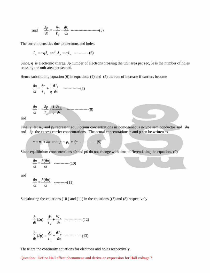
Question: Define Hall effect phenomena and derive an expression for Hall voltage ?
Answer:Hall effect:
When a magnetic field is applied perpendicular to a current carrying conductor or semiconductor, avoltage is developed across the specimen in a direction perpendicular to both the current and the magneticfield. This phenomenon is called the Hall effect and the voltage so developed is called Hall voltage.
As shown in figure 1 , consider a uniform thick metal strip placed with its length parallel to X-axis. Let acurrent I is passed in the conductor along X-axis and a magnetic field B is established along X-axis. Due tothe magnetic field, the charge carriers experience a force F D perpendicular to X-Z plane (i.e along Y-axis)The direction of this force is given by Fleming left hand rule. IF the charge carriers are electrons then theywill experience a force in the negative direction of Y. Hence, they will be accumulated on the back surfaceof the strip. Due to this fact the back surface will be charged negatively while the front surface will becharged positively. Thus, a transverse potential difference is created/ This emf is known as Hall emf. Ifthe charge carriers are positively charged particles like protons of holes, the sign of emf is reversed. Thus,the nature of charge carriers can be found by determining the sign of Hall emf which can be measured by apotentiometer. Experiments showed that the charge carriers in metals are electrons while the charge carriersin p-type semiconductors are holes.
Magnetic deflecting force
( )BvqF dp ×= --------------(1)
Hall electric deflecting force
qFn = HE --------------(2)
When an equilibrium is reached, the magnetic deflecting forces on the charge carriers are balanced by theelectric forces due to electric field.
Hence, the net force on the charge carriers become zero and from equation (1) and (2)
( ) qBvq d +× 0=nE
or( )BvE dH ×−=
In terms of magnitude BvE dH =
Where Vd is drift velocity of electrons
The relation between current density and drift velocity is
nq
Jvd = ------------(3)
Where n is the number of charge carriers per unit volume.
Substituting equation (3) in equation (4), the Hall emf
JBnq
jEH
= --------------(4)
If VH is the Hall voltage in equilibrium, the Hall electric field,
=d
VE H
H -----(5)
Where d is width of metal strip.
Thus measuring the current I in the slab, the current density can be calculated by using the formula (i/A)where A is the area of cross section of the slab. The magnetic field can be measured by a Gauss-meter. SOon substituting the values of EH, J and B in equations (4), the value of (1/nq) can be calculated.
Hall coefficient RH is defined asJB
ER H
H = ---------(6)
From equation (4)
nqJB
EH 1=
nqRH
1=
The Hall coefficient is negative when the charge carriers are electrons and poitive when the charge carriersare holes.
Question: Write short notes on direct and indirect band gap semiconductors?
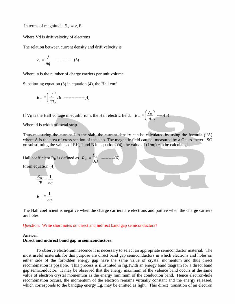
Answer:Direct and indirect band gap in semiconductors:
To observe electroluminescence it is necessary to select an appropriate semiconductor material. Themost useful materials for this purpose are direct band gap semiconductors in which electrons and holes oneither side of the forbidden energy gap have the same value of crystal momentum and thus directrecombination is possible. This process is illustrated in fig.1with an energy band diagram for a direct bandgap semiconductor. It may be observed that the energy maximum of the valence band occurs at the samevalue of electron crystal momentum as the energy minimum of the conduction band. Hence electron-holerecombination occurs, the momentum of the electron remains virtually constant and the energy released,which corresponds to the bandgap energy Eg, may be emitted as light. This direct transition of an electron
across the energy gap provides an efficient mechanism of photon emission and the average timetime theminority carrier remains in agree state before recombination. Some of the examples of direct band gapsemiconductors GaAs, Ge, InSb, GaSb etc.
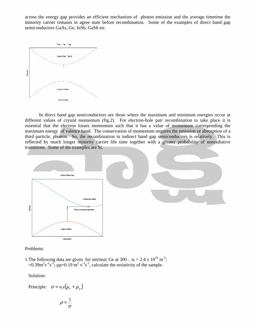
In direct band gap semiconductors are those where the maximum and minimum energies occur atdifferent values of crystal momentum (fig.2). For electron-hole pair recombination to take place it isessential that the electron losses momentum such that it has a value of momentum corresponding themaximum energy of valence band. The conservation of momentum requires the emission or absorption of athird particle, phonon. So, the recombination in indirect band gap semiconductors is relatively. This isreflected by much longer minority carrier life time together with a greater probability of nonradiativetransitions. Some of the examples are Si.
Problems:
1.The following data are given for intrinsic Ge at 300 . ni = 2.4 x 10¹⁹ m-3;=0.39m2v-1s-1; µp=0.19 m2 v-1s-1, calculate the resistivity of the sample.
Solution:
Principle: ( )peien µµσ +=
σρ 1=
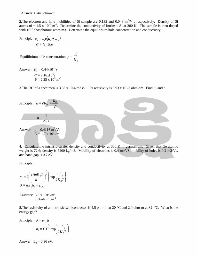
Answer: 0.448 ohm-cm
2.The electron and hole mobilities of Si sample are 0.135 and 0.048 m2/V-s respectively. Density of Siatoms ni = 1.5 x 10¹⁶ m-3. Determine the conductivity of Intrinsic Si at 300 K. The sample is then dopedwith 1023 phosphorous atom/m3. Determine the equilibrium hole concentration and conductivity.
Principle: ( )peii en µµσ +=eN nD µσ =
Equilibrium hole concentrationD
i
N
np
2
=
Answer: sxi31044.0 −=σsx 31016.2=σ
P = 2.25 x 10⁹ m-3
3.The RH of a specimen is 3.66 x 10⁻⁴ m3 c-1. Its resistivity is 8.93 x 10 -3 ohm-cm. Find µ and n.
Principle :ρ
σµ HH
RR ==
eRn
H
1=
Answer: µ = 0.4116 m2/VsN = 1.7 x 10²²/m3
4. Calculate the intrinsic carrier density and conductivity at 300 K in germanium. Given that Ge atomicweight is 72.6; density is 5400 kg/m3. Mobility of electrons is 0.4 mr/VS, mobility of holes is 0.2 m2/Vs,and band gap is 0.7 eV,
Principle:
−
=TK
E
h
TmKn
B
gBi 2
exp2
22
3
2
π
( )peien µµσ +=
Answers: 3.5 x 10¹⁹/m3
3.36ohm-1cm-1
5.The resistivity of an intrinsic semiconductor is 4.5 ohm-m at 20 °C and 2.0 ohm-m at 32 °C. What is theenergy gap?
Principle: µσ ien=
−=
TK
ECTn
B
gi 2
exp2
3
Answer: Eg = 0.96 eV.
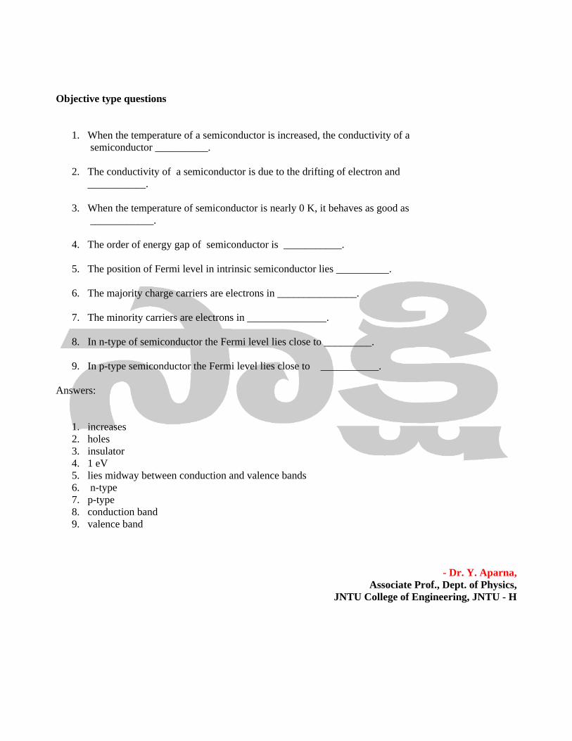
Objective type questions
1. When the temperature of a semiconductor is increased, the conductivity of asemiconductor __________.
2. The conductivity of a semiconductor is due to the drifting of electron and___________.
3. When the temperature of semiconductor is nearly 0 K, it behaves as good as____________.
4. The order of energy gap of semiconductor is ___________.
5. The position of Fermi level in intrinsic semiconductor lies __________.
6. The majority charge carriers are electrons in _______________.
7. The minority carriers are electrons in _______________.
8. In n-type of semiconductor the Fermi level lies close to _________.
9. In p-type semiconductor the Fermi level lies close to ___________.
Answers:
1. increases2. holes3. insulator4. 1 eV5. lies midway between conduction and valence bands6. n-type7. p-type8. conduction band9. valence band
- Dr. Y. Aparna,Associate Prof., Dept. of Physics,
JNTU College of Engineering, JNTU - H