Semiconductor Devices - 2014€¦ · Semiconductor Devices - 2014 Lecture Course Part of SS Module...
18
Semiconductor Devices - 2014 Lecture Course Part of SS Module PY4P03 Dr. P. Stamenov School of Physics and CRANN, Trinity College, Dublin 2, Ireland Hilary Term, TCD 31 th of Feb ‘14
Transcript of Semiconductor Devices - 2014€¦ · Semiconductor Devices - 2014 Lecture Course Part of SS Module...

Semiconductor Devices - 2014
Lecture Course Part of
SS Module PY4P03
Dr. P. Stamenov
School of Physics and CRANN, Trinity College, Dublin 2, Ireland
Hilary Term, TCD 31th of Feb ‘14

Overview of JFETs and MOSFETs
• Realistic fabrication (process flow example) • The FET Family Tree • FET Structures • JFET Modelling • MOSFET Modelling
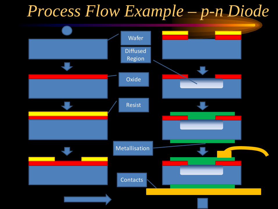
Oxide
Resist
Diffused Region
Metallisation
Contacts
Wafer
Process Flow Example – p-n Diode

Unipolar FETs’ Family Free
FET
JFET
MESFET
MOSFET
Si JFET
GaAs JFET
Si MESFET GaAs MESFET
InP MESFET
Si MOSFET
GaAs MOSFET
Single Channel V- Groove Multichannel
Single Gate Multiple Gate Interdigitals NMOS, PMOS CMOS HMOS DMOS, DIMOS VMOS SOS, SOI
Diffused Grown Heterojunction
Remarks on FETs • Essentially unipolar devices – the current flow (either holes or
electrons) between two electrodes (source and drain) is controlled by the potential difference to a third electrode (gate).
• Close (closer) to ohmic behaviour. Linear or square law. Lower total harmonic distortion and intermodulation distortion.
• Much higher input impedance. Lower input currents. Simpler matching to microwave circuits.
• Negative temperature coefficient. Self-limiting, with a much lower probability for a thermal runaway or breakdown.
• No minority carrier storage effects – higher switching speeds and higher cutoff frequencies.
• Conceptually simpler, with close to equilibrium carrier concentrations, virtually no carrier injection or extraction.
• Could have been the first ones to be realized...
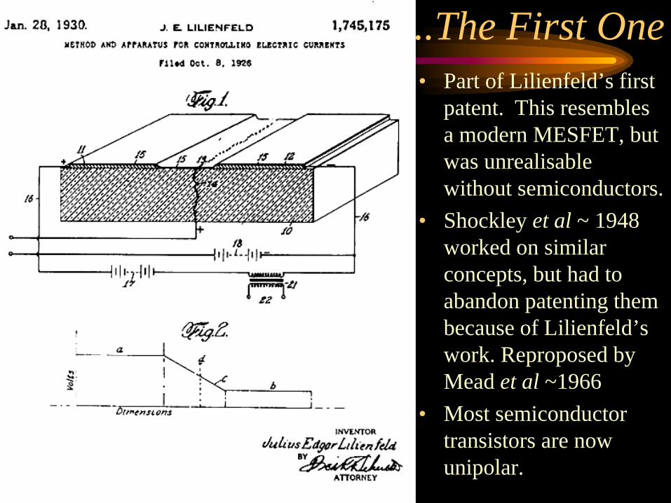
...The First One • Part of Lilienfeld’s first
patent. This resembles a modern MESFET, but was unrealisable without semiconductors.
• Shockley et al ~ 1948 worked on similar concepts, but had to abandon patenting them because of Lilienfeld’s work. Reproposed by Mead et al ~1966
• Most semiconductor transistors are now unipolar.
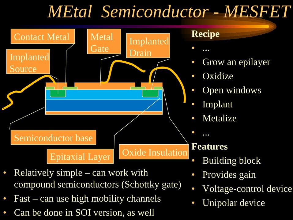
MEtal Semiconductor - MESFET
Semiconductor base
Contact Metal
Oxide Insulation
Implanted Drain
Epitaxial Layer
Metal Gate
Implanted Source
Recipe • ... • Grow an epilayer • Oxidize • Open windows • Implant • Metalize • ... Features • Building block • Provides gain • Voltage-control device • Unipolar device
• Relatively simple – can work with compound semiconductors (Schottky gate)
• Fast – can use high mobility channels • Can be done in SOI version, as well
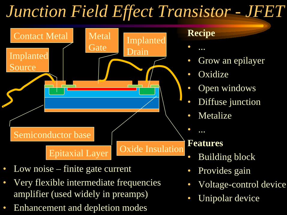
Junction Field Effect Transistor - JFET
Semiconductor base
Contact Metal
Oxide Insulation
Implanted Drain
Epitaxial Layer
Metal Gate
Implanted Source
Recipe • ... • Grow an epilayer • Oxidize • Open windows • Diffuse junction • Metalize • ... Features • Building block • Provides gain • Voltage-control device • Unipolar device
• Low noise – finite gate current • Very flexible intermediate frequencies
amplifier (used widely in preamps) • Enhancement and depletion modes
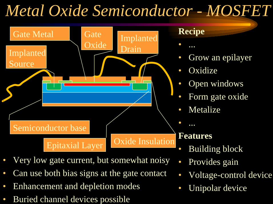
Metal Oxide Semiconductor - MOSFET
Semiconductor base
Gate Metal
Oxide Insulation
Implanted Drain
Epitaxial Layer
Gate Oxide
Implanted Source
Recipe • ... • Grow an epilayer • Oxidize • Open windows • Form gate oxide • Metalize • ... Features • Building block • Provides gain • Voltage-control device • Unipolar device
• Very low gate current, but somewhat noisy • Can use both bias signs at the gate contact • Enhancement and depletion modes • Buried channel devices possible
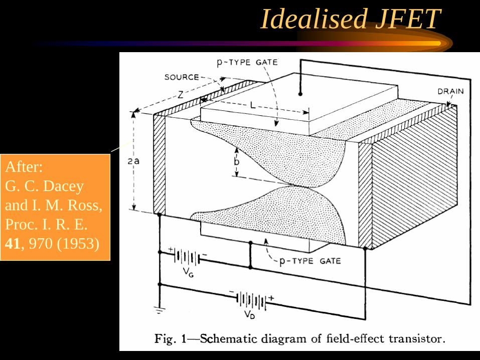
Idealised JFET
After: G. C. Dacey and I. M. Ross, Proc. I. R. E. 41, 970 (1953)
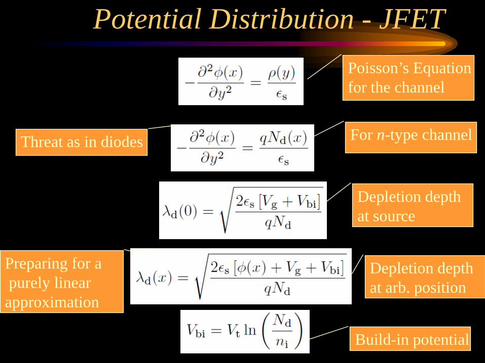
Potential Distribution - JFET Poisson’s Equation for the channel
For n-type channel
Depletion depth at source
Depletion depth at arb. position
Build-in potential
Threat as in diodes
Preparing for a purely linear approximation
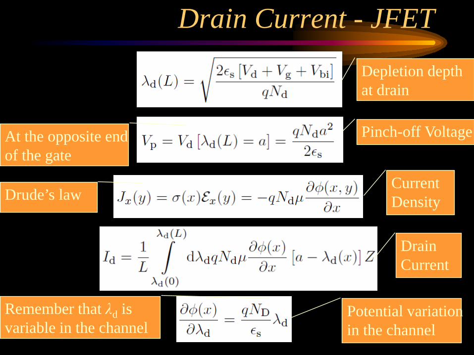
Drain Current - JFET
Depletion depth at drain
Pinch-off Voltage
Current Density
Drain Current
Potential variation in the channel
At the opposite end of the gate
Drude’s law
Remember that λd is variable in the channel
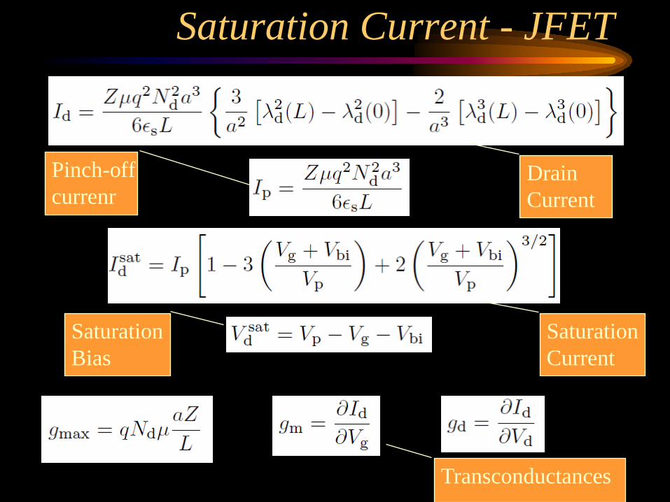
Saturation Current - JFET
Drain Current
Pinch-off currenr
Saturation Current
Saturation Bias
Transconductances

Transconductance and Drain Current
Drain Conductance
Gate Transconductance
Threshold Voltage
Approximate Drain Current Expression. REMEMBER!

The MOSFET
After: S. M. Sze, Physics of Semiconductor Devices, 2nd edition
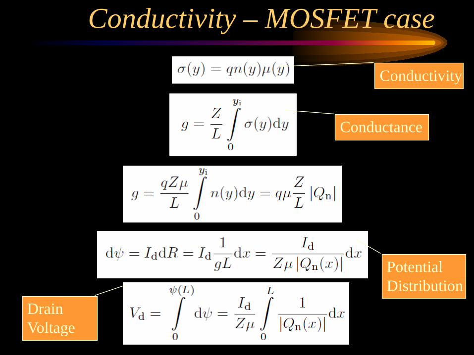
Conductivity – MOSFET case
Conductivity
Conductance
Potential Distribution
Drain Voltage
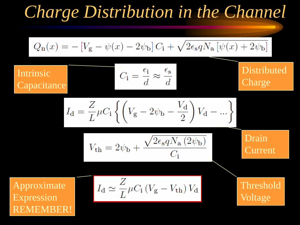
Charge Distribution in the Channel
Distributed Charge
Intrinsic Capacitance
Drain Current
Threshold Voltage
Approximate Expression REMEMBER!
Thanks and Acknowledgements
Thank You Very Much for Your Attention!