
Semiconductor Devices - 2014 Devices - 2014 Lecture Course Part of ... The Tunnel Diode – IV...
14
Semiconductor Devices - 2014 Lecture Course Part of SS Module PY4P03 Dr. P. Stamenov School of Physics and CRANN, Trinity College, Dublin 2, Ireland Hilary Term, TCD 14 th of Feb ‘14
Transcript of Semiconductor Devices - 2014 Devices - 2014 Lecture Course Part of ... The Tunnel Diode – IV...
Semiconductor Devices - 2014
Lecture Course Part of
SS Module PY4P03
Dr. P. Stamenov
School of Physics and CRANN, Trinity College, Dublin 2, Ireland
Hilary Term, TCD 14th of Feb ‘14
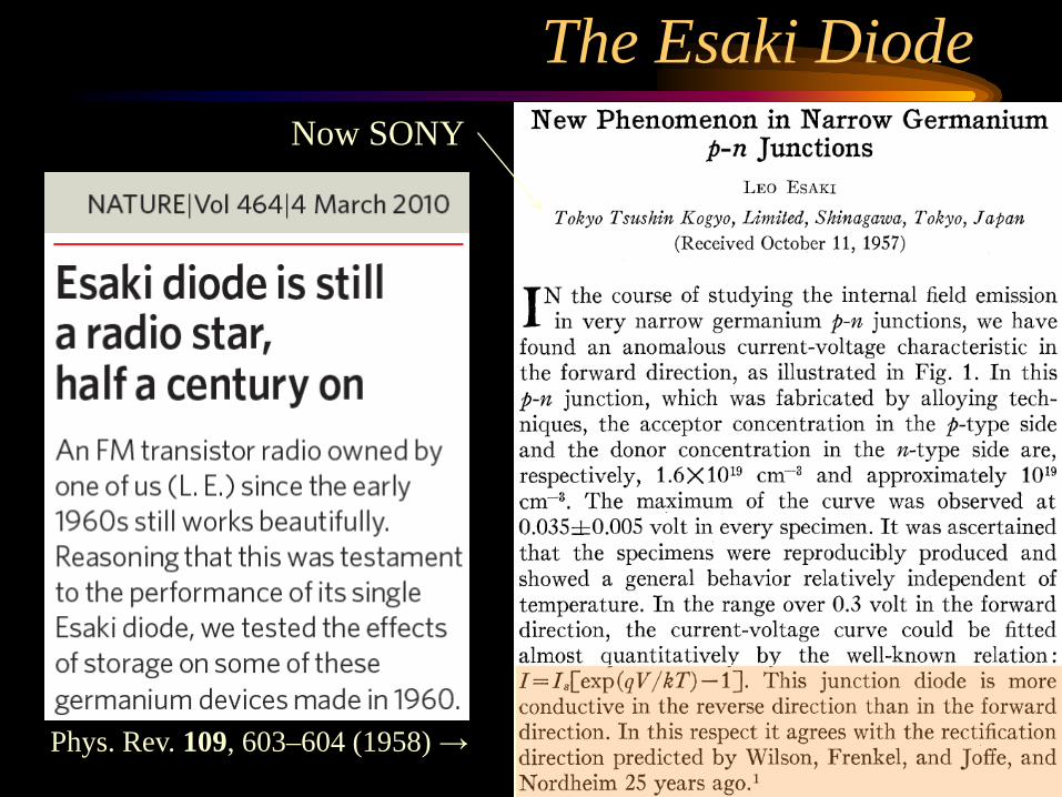
The Esaki Diode
Phys. Rev. 109, 603–604 (1958) →
Now SONY
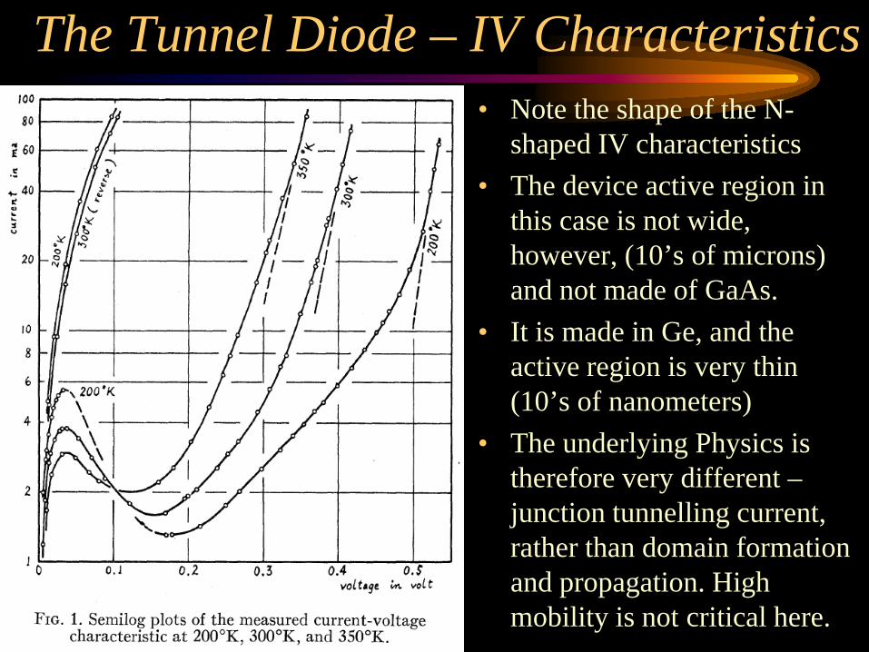
The Tunnel Diode – IV Characteristics • Note the shape of the N-
shaped IV characteristics • The device active region in
this case is not wide, however, (10’s of microns) and not made of GaAs.
• It is made in Ge, and the active region is very thin (10’s of nanometers)
• The underlying Physics is therefore very different – junction tunnelling current, rather than domain formation and propagation. High mobility is not critical here.
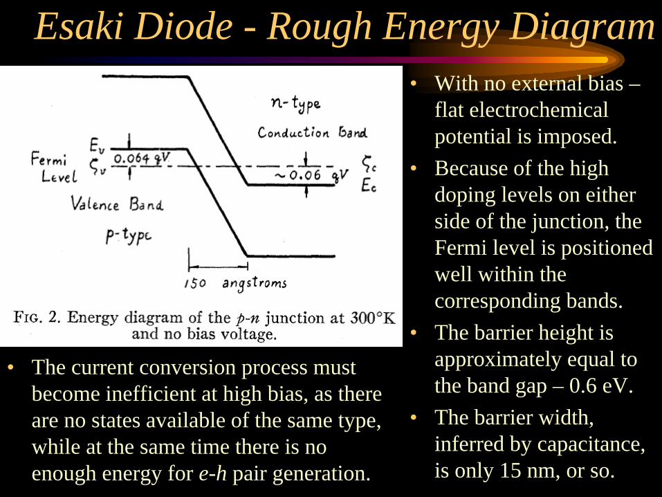
Esaki Diode - Rough Energy Diagram • With no external bias –
flat electrochemical potential is imposed.
• Because of the high doping levels on either side of the junction, the Fermi level is positioned well within the corresponding bands.
• The barrier height is approximately equal to the band gap – 0.6 eV.
• The barrier width, inferred by capacitance, is only 15 nm, or so.
• The current conversion process must become inefficient at high bias, as there are no states available of the same type, while at the same time there is no enough energy for e-h pair generation.
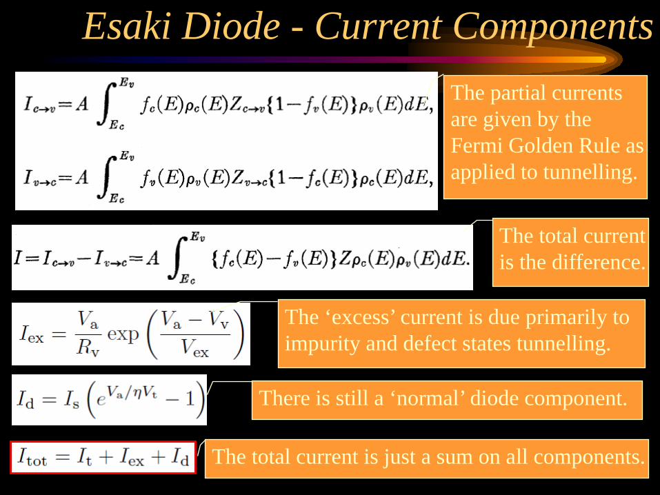
Esaki Diode - Current Components The partial currents are given by the Fermi Golden Rule as applied to tunnelling.
The total current is the difference.
The ‘excess’ current is due primarily to impurity and defect states tunnelling.
There is still a ‘normal’ diode component.
The total current is just a sum on all components.
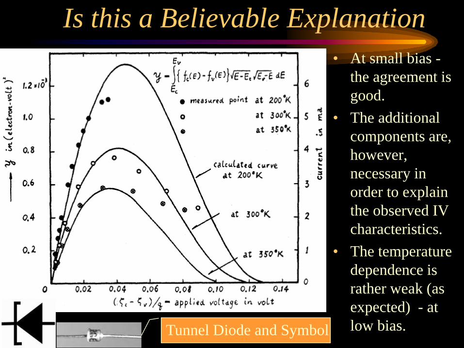
Is this a Believable Explanation • At small bias -
the agreement is good.
• The additional components are, however, necessary in order to explain the observed IV characteristics.
• The temperature dependence is rather weak (as expected) - at low bias. Tunnel Diode and Symbol
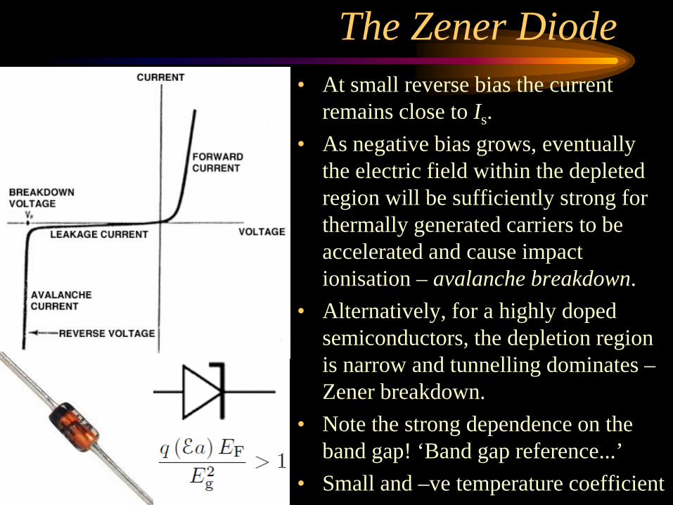
The Zener Diode • At small reverse bias the current
remains close to Is. • As negative bias grows, eventually
the electric field within the depleted region will be sufficiently strong for thermally generated carriers to be accelerated and cause impact ionisation – avalanche breakdown.
• Alternatively, for a highly doped semiconductors, the depletion region is narrow and tunnelling dominates – Zener breakdown.
• Note the strong dependence on the band gap! ‘Band gap reference...’
• Small and –ve temperature coefficient
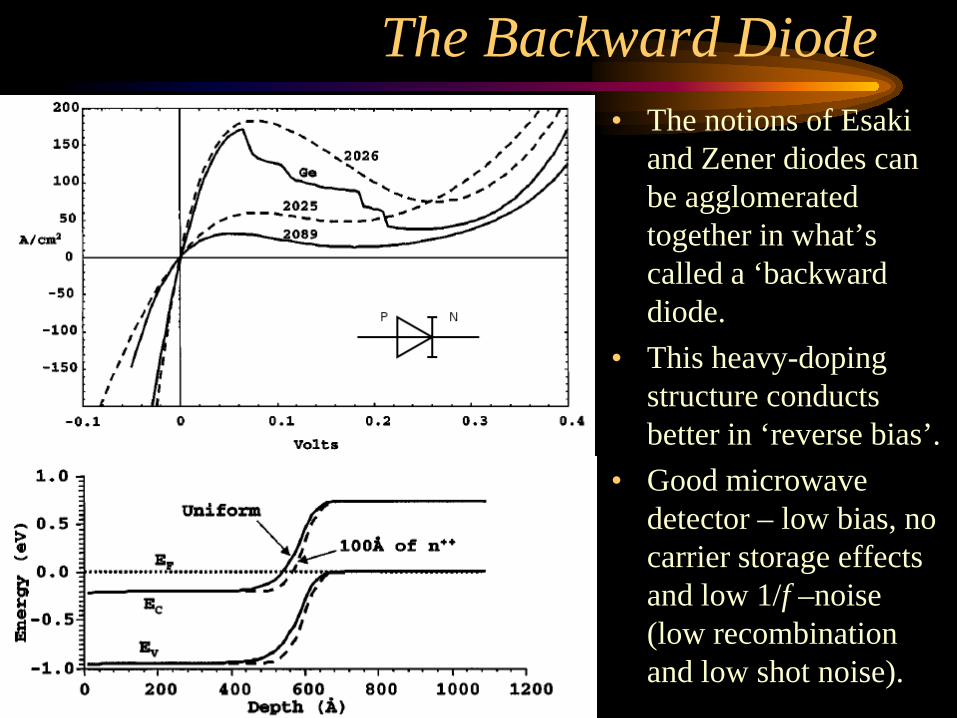
The Backward Diode • The notions of Esaki
and Zener diodes can be agglomerated together in what’s called a ‘backward diode.
• This heavy-doping structure conducts better in ‘reverse bias’.
• Good microwave detector – low bias, no carrier storage effects and low 1/f –noise (low recombination and low shot noise).
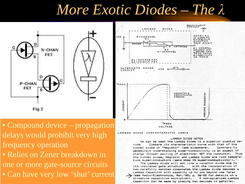
More Exotic Diodes – The λ
• Compound device – propagation delays would prohibit very high frequency operation • Relies on Zener breakdown in one or more gate-source circuits • Can have very low ‘shut’ current
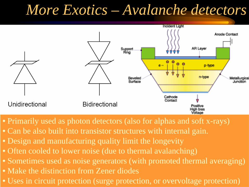
More Exotics – Avalanche detectors
• Primarily used as photon detectors (also for alphas and soft x-rays) • Can be also built into transistor structures with internal gain. • Design and manufacturing quality limit the longevity • Often cooled to lower noise (due to thermal avalanching) • Sometimes used as noise generators (with promoted thermal averaging) • Make the distinction from Zener diodes • Uses in circuit protection (surge protection, or overvoltage protection)
Heteroepitaxy and Heterostructures • There are now many types of both unipolar and bipolar devices with
two or more different compound semiconductors in the same device. • There are methods for obtaining very high frequency responses with
these structures. These will be discussed later. • These devices are usually made by heteroepitaxial techniques, in
which the epilayer-substrate crystal lattices must be matched up, as in homoepitaxy.
• For lattice-matched epitaxy, e.g. AlxGa1-xAs on GaAs, the lattice constants are the same to within 0.13% for any value of x between 0 and 1 – case (i) on next slide.
• But in a significantly mismatched case, and to achieve new device possibilities, the epilayer should be strained (+ve or –ve), by the substrate to 'force' a match (strained-layer epitaxy, with pseudomorphic layers) – case (ii) – whereas misfit dislocations, relieving the strain, degrade device performance – case (iii).
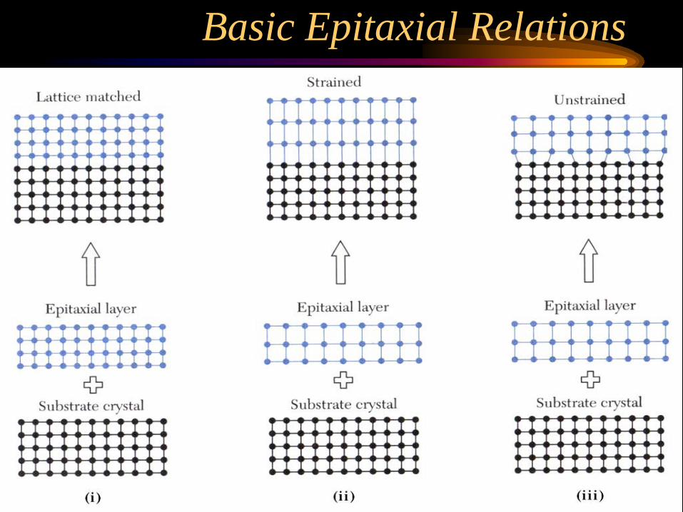
Basic Epitaxial Relations
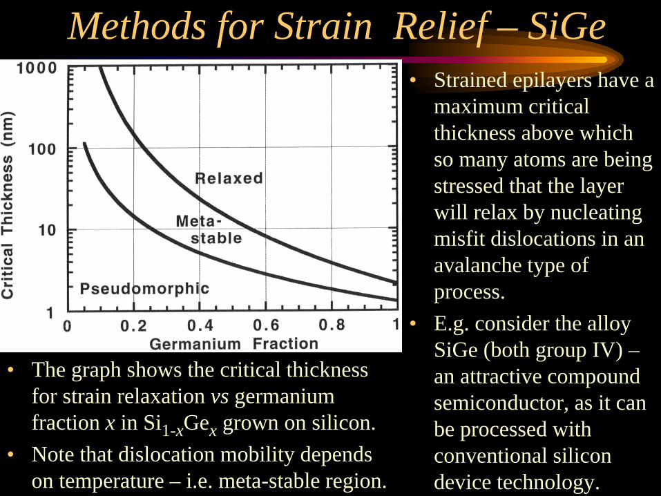
Methods for Strain Relief – SiGe • Strained epilayers have a
maximum critical thickness above which so many atoms are being stressed that the layer will relax by nucleating misfit dislocations in an avalanche type of process.
• E.g. consider the alloy SiGe (both group IV) – an attractive compound semiconductor, as it can be processed with conventional silicon device technology.
• The graph shows the critical thickness for strain relaxation vs germanium fraction x in Si1-xGex grown on silicon.
• Note that dislocation mobility depends on temperature – i.e. meta-stable region.
Thanks and Acknowledgements
Thank You Very Much for Your Attention!