diode - University of California, Berkeleyicbook.eecs.berkeley.edu/.../files/diode.pdf · ·...
22
1 CHAPTER 1 THE DIODE 1.1 The Diode 1.1.1 A First Glance at the Device 1.1.2 Static Behavior 1.1.3 Dynamic, or Transient, Behavior 1.1.4 The Actual Diode—Secondary Effects A Short Treatise on Diodes 1.1.5 The SPICE Diode Model diode.fm Page 1 Friday, April 4, 2003 8:49 AM
Transcript of diode - University of California, Berkeleyicbook.eecs.berkeley.edu/.../files/diode.pdf · ·...

1
C H A P T E R
1
T H E D I O D E
1.1 The Diode
1.1.1 A First Glance at the Device
1.1.2 Static Behavior
1.1.3 Dynamic, or Transient, Behavior
1.1.4 The Actual Diode—Secondary Effects
A Short Treatise on Diodes
1.1.5 The SPICE Diode Model
diode.fm Page 1 Friday, April 4, 2003 8:49 AM

2 THE DIODE Chapter 1
1.1 The Diode
Although diodes rarely occur directly in the schematic diagrams of present-day digitalgates, they are still omnipresent. For instance, each MOS transistor implicitly contains anumber of reverse-biased diodes. Diodes are used to protect the input devices of an ICagainst static charges. Also, a number of bipolar gates use diodes as a means to adjustvoltage levels. Therefore, a brief review of the basic properties and device equations of thediode is appropriate.
1.1.1 A First Glance at the Device
The pn-junction diode is the simplest of the semiconductor devices. Figure 1.1a shows across-section of a typical pn-junction. It consists of two homogeneous regions of p- and n-type material, separated by a region of transition from one type of doping to another,which is assumed thin. Such a device is called a step or abrupt junction. The p-type mate-rial is doped with acceptor impurities (such as boron), which results in the presence ofholes as the dominant or majority carriers. Similarly, the doping of silicon with donorimpurities (such as phosphorus or arsenic) creates an n-type material, where electrons arethe majority carriers. Aluminum contacts provide access to the p- and n-terminals of thedevice. The circuit symbol of the diode, as used in schematic diagrams, is introduced inFigure 1.1c.
n
p
Figure 1.1 Abrupt pn-junction diode and its schematic symbol.
p
n
B ASiO2
Al
A
B
AlA
B
(a) Cross-section of pn-junction in an IC process
(c) Diode symbol(b) One-dimensional representation
diode.fm Page 2 Friday, April 4, 2003 8:49 AM
Section 1.1 The Diode 3
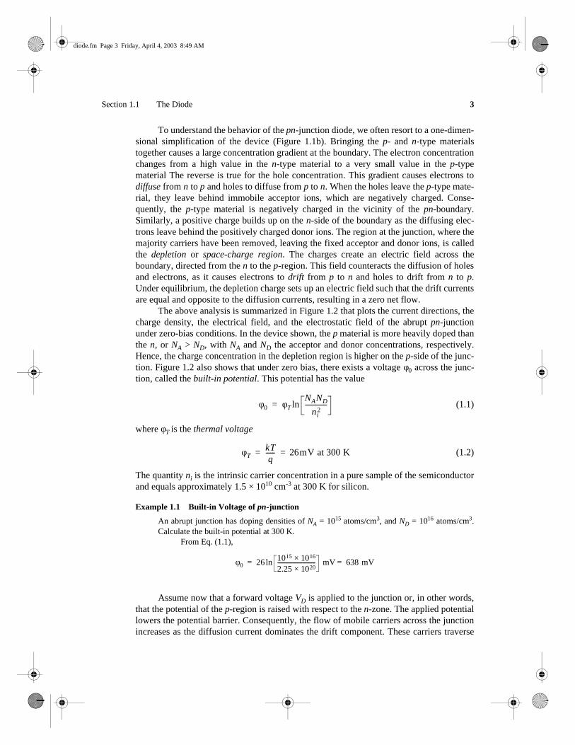
To understand the behavior of the pn-junction diode, we often resort to a one-dimen-sional simplification of the device (Figure 1.1b). Bringing the p- and n-type materialstogether causes a large concentration gradient at the boundary. The electron concentrationchanges from a high value in the n-type material to a very small value in the p-typematerial The reverse is true for the hole concentration. This gradient causes electrons todiffuse from n to p and holes to diffuse from p to n. When the holes leave the p-type mate-rial, they leave behind immobile acceptor ions, which are negatively charged. Conse-quently, the p-type material is negatively charged in the vicinity of the pn-boundary.Similarly, a positive charge builds up on the n-side of the boundary as the diffusing elec-trons leave behind the positively charged donor ions. The region at the junction, where themajority carriers have been removed, leaving the fixed acceptor and donor ions, is calledthe depletion or space-charge region. The charges create an electric field across theboundary, directed from the n to the p-region. This field counteracts the diffusion of holesand electrons, as it causes electrons to drift from p to n and holes to drift from n to p.Under equilibrium, the depletion charge sets up an electric field such that the drift currentsare equal and opposite to the diffusion currents, resulting in a zero net flow.
The above analysis is summarized in Figure 1.2 that plots the current directions, thecharge density, the electrical field, and the electrostatic field of the abrupt pn-junctionunder zero-bias conditions. In the device shown, the p material is more heavily doped thanthe n, or NA > ND, with NA and ND the acceptor and donor concentrations, respectively.Hence, the charge concentration in the depletion region is higher on the p-side of the junc-tion. Figure 1.2 also shows that under zero bias, there exists a voltage φ0 across the junc-tion, called the built-in potential. This potential has the value
(1.1)
where φT is the thermal voltage
(1.2)
The quantity ni is the intrinsic carrier concentration in a pure sample of the semiconductorand equals approximately 1.5 × 1010 cm-3 at 300 K for silicon.
Example 1.1 Built-in Voltage of pn-junction
An abrupt junction has doping densities of NA = 1015 atoms/cm3, and ND = 1016 atoms/cm3.Calculate the built-in potential at 300 K.
From Eq. (1.1),
Assume now that a forward voltage VD is applied to the junction or, in other words,that the potential of the p-region is raised with respect to the n-zone. The applied potentiallowers the potential barrier. Consequently, the flow of mobile carriers across the junctionincreases as the diffusion current dominates the drift component. These carriers traverse
φ0 φTNAND
ni2
--------------ln=
φTkTq
------ 26mV at 300 K= =
φ0 26 1015 1016×2.25 1020×---------------------------ln mV 638 mV= =
diode.fm Page 3 Friday, April 4, 2003 8:49 AM

4 THE DIODE Chapter 1
the depletion region and are injected into the neutral n- and p-regions, where they becomeminority carriers. Under the assumption that no voltage gradient exists over the neutralregions, which is approximately the case for most modern devices, these minority carrierswill diffuse through the region as a result of the concentration gradient until they getrecombined with a majority carrier. The net result is a current flowing through the diodefrom the p-region to the n-region. The most important property of this current is its expo-nential dependence upon the applied bias voltage.
On the other hand, when a reverse voltage VD is applied to the junction or when thepotential of the p-region is lowered with respect to the n-region, the potential barrier israised. This results in a reduction in the diffusion current, and the drift current becomesdominant. A current flows from the n-region to the p-region. Since the number of minoritycarriers in the neutral regions (electrons in the p-zone, holes in the n-region) is very small,this drift current component is virtually ignorable. It is fair to state that in the reverse-biasmode the diode operates as a nonconducting, or blocking, device. The diode thus acts as aone-way conductor. This is illustrated in Figure 1.3, which plots the diode current ID as a
Hole diffusion
Electron diffusion
p n
Hole drift
Electron drift
Chargedensity
Distance
x+
-
Electrical
xfield
x
Potential V
E
ρ
W2-W1 φ0
Figure 1.2 The abrupt pn-junction under equilibrium bias.
(a) Current flow
(b) Charge density
(c) Electric field
(d) Electrostatic potential
diode.fm Page 4 Friday, April 4, 2003 8:49 AM

Section 1.1 The Diode 5
function of the bias voltage VD. The exponential behavior for positive-bias voltages isshown in Figure 1.3b, where the current is plotted on a logarithmic scale. The currentincreases by a factor of 10 for every extra 60 mV (= 2.3 φT) of forward bias. At small volt-age levels (VD < 0.15 V), a deviation from the exponential dependence can be observed,which is due to the recombination of holes and electrons in the depletion region as dis-cussed in more detail later in the chapter.
After this intuitive introduction, we present analytical expressions for the behaviorof the pn-junction. A distinction is made between the static (or steady-state) and thedynamic (or transient) behavior of the device.
1.1.2 Static Behavior
From earlier encounters with semiconductor devices [e.g., Sedra87], the reader is mostprobably familiar with the ideal diode equation, which relates the current through thediode ID to the diode bias voltage VD
(1.3)
IS represents a constant value, called the saturation current of the diode. Under reverse-bias conditions, where VD << 0, ID ≈ −IS and equals the reverse-bias leakage current. φT isthe thermal voltage of Eq. (1.2) and is equal to 26 mV at room temperature. The remainderof this section presents a physical background for this equation.
Forward Bias
When a positive voltage is applied to the junction, mobile carriers drift through the deple-tion region and are injected into the neutral regions, where they become excess minoritycarriers and diffuse in the direction of the terminal connections. It is the distribution ofthese excess minority carriers that dictates the static behavior of the pn-diode. Figure 1.4shows the minority carrier concentrations in the neutral region near a pn-junction for the
Figure 1.3 Diode current as a function of the bias voltage VD.
0.0 0.2 0.4 0.6 0.810–15
10–10
10–5
100
I D (A
)
–1.0 –0.5 0.0 0.5 1.0
VD (V)
–0.5
0.5
1.5
2.5I D
(m
A)
VD (V)
(a) On a linear scale (b) On a logarithmic scale (forward bias only)
2.3 φT V / decade
Deviation due to recombination
current
ID IS eVD φT⁄ 1–( )=
diode.fm Page 5 Friday, April 4, 2003 8:49 AM

6 THE DIODE Chapter 1
forward-bias condition. Observe that the majority carrier concentrations have to proceedalong the same line, because charge neutrality dictates that any local increase in the elec-tron (hole) concentration is matched by a similar increase in the hole (electron) density.While the fractional increase of the minority carrier concentration is substantial, it islargely ignorable for the majority carriers.
Figure 1.4 shows a linear decay in the minority carrier concentrations when movingaway from the junction. At the metal contacts (which can be assumed to be infinitesources or sinks of holes or electrons), the minority carrier concentrations are at their equi-librium values (np0 and pn0), independent of the applied bias. The linear decay model isvalid under the assumption that the width of the n- or p-regions is sufficiently small so thatinjected minority carriers diffuse to the metal contact before recombining with majoritycarriers. This operation condition is called the short-base diode model and is valid formost contemporary semiconductor diodes.
The gradient in the minority concentrations causes a diffusion current in the neutral(also called bulk) regions that is proportional to that gradient. The constant of proportion-ality is called the diffusion coefficient (Dp and Dn for holes and electrons, respectively).Based on these observations, an expression for the diode current can be derived. In thisderivation, we initially consider the n-region only. Similar expressions can be derived forthe p-region.
(1.4)
with
(1.5)
where pn(x) represents the hole concentration in the n-region as a function of the positionx, AD is the junction area, and q is the electron (hole) charge. Combining the two equationsresults in an expression of the diode current as a function of the minority carrier concen-
Figure 1.4 Minority carrier concentrations in the neutral region near an abrupt pn-junction underforward-bias conditions.
x
pn0
np0
–W1 W20
p n(W
2)
n-regionp-region Wn–Wp
pn(x)
np(x)
Met
al c
onta
ct to
n-r
egio
n
Met
al c
onta
ct to
p-r
egio
n
Minority carrier concentration
ID p, xddpn∼ qADDp xd
dpn–=
pn x( )pn W2( ) pn0–
Wn W2–------------------------------- x–
pn W2( )Wn pn0W2–Wn W2–
-----------------------------------------------+=
diode.fm Page 6 Friday, April 4, 2003 8:49 AM

Section 1.1 The Diode 7
tration at the boundary of the depletion region. The latter is determined by the law of thejunction, which states that the concentration at the edge of the depletion region is an expo-nential function of the applied bias voltage
(1.6)
with pn0 the hole concentration in the n-region under equilibrium conditions. For NA >> ni,the equilibrium minority hole concentration (in the n-region) is obtained from the follow-ing expression
(1.7)
and, similarly, for the p-region
(1.8)
Combining Equations (1.4), (1.5) and (1.6) yields the diode current,
(1.9)
Repeating the same analysis for the p-region and summing the p and n current-con-tributions produces the ideal diode current expression of Eq. (1.3). It also yields an expres-sion for the saturation current IS
(1.10)
Keep in mind that the above equation is based on a number of assumptions, whichmight not be valid for all actual devices. First of all, it is assumed that the length of theneutral regions is short enough that recombination does not occur (short-base diodemodel). For this to be valid, the widths of the p- and n-regions must be substantiallysmaller than a material constant called the diffusion length (denoted as Lp and Ln for holesand electrons, respectively). If this is not the case, the diode becomes of the long-basetype. Minority carriers diffusing through the neutral region gradually recombine withmajority carriers. This affects the minority-carrier concentration as illustrated in Figure1.5. Instead of a linear decay, the concentration drops in an exponential fashion. In onediffusion length, the excess minority concentration drops to 1/e (= 0.37) of its originalvalue. After a few diffusion lengths, virtually all injected carriers have recombined, andthe minority carrier concentration reaches its thermal equilibrium value. The current equa-tion remains essentially unchanged. The only modification is that the Wn and Wp parame-ters in the saturation current (Eq. (1.10)) are replaced by the diffusion lengths Lp and Ln.
Other assumptions are that the resistance of the neutral regions is negligible, andthat the minority carrier injection levels are substantially lower than the majority concen-tration levels (low-injection condition). Later in the chapter we discuss how violatingthese conditions affects the device operation.
Eq. (1.10) clearly shows that the diode current is the composite result of a hole andan electron current. In most practical diodes, one of the sides has a substantially lighterdoping level and hence produces a larger number of minority carriers. The corresponding
pn W2( ) pn0eVD φT⁄=
pn0 ni2 ND⁄≈
np0 ni2 NA⁄≈
IDp qADDppn0
Wn W2–-------------------- eVD φT⁄ 1–( )=
IS qADDppn0
Wn W2–--------------------
Dnnp0
Wp W1–--------------------+
=
diode.fm Page 7 Friday, April 4, 2003 8:49 AM

8 THE DIODE Chapter 1
current component dominates the overall value. For instance, in the example of Figure 1.2,the p-region has a heavier doping than the n-region. Consequently, pn0 >> np0, and the holecurrent dominates.
Problem 1.1 Diode Current
For a diode with the following properties, compute the saturation current IS. Also, solve VDfor ID = 0.1 mA, assuming that φT = 26 mV.
AD = 9 µm2, ND = 5 × 1015 cm−3, NA= 2.5 × 1016 cm−3, φ0 = 0.795 V, Dn = 25 cm2/sec, Dp = 10 cm2/sec, Wn = 5 µm and Wp = 0.7 µm, W2 = 0.15 µm and W1= 0.03 µm. ni = 1.5 × 1010 cm−3 and q = 1.6 × 10⁻¹⁹ C. Also, Ln = 5 µm and Lp = 31 µm.
Reverse Bias
When applying a reverse-bias voltage to the junction, the ideal diode equation predicts thatthe diode current ID approaches −IS for |VD| >> φT. This is readily understood when analyz-ing the minority carrier concentration distribution under reverse-bias conditions, as shownin Figure 1.6.1 From the law of the junction (which is equally valid under reverse-bias con-
1 It is worth observing that all equations derived for the forward-bias apply just as well under reverse-biasconditions.
Figure 1.5 Minority carrier concentrations in the n-region near a pn-junction.
x
x
pn0
pn0
Lp
Wn
pn(x)
pn(x)
Wn
(a) Short-base diode: Wn << Lp
(b) Long-base diode: Wn >> Lp
diode.fm Page 8 Friday, April 4, 2003 8:49 AM

Section 1.1 The Diode 9
ditions), it can be derived that the concentration of minority carriers at the depletion-regionboundaries is small and actually approaches 0 when sufficient reverse bias is applied. Atthe metallic contacts, the concentration is restored to the thermal equilibrium value.
The resulting gradient causes a diffusion of minority carriers towards the junction.Once they reach the depletion region they are swept across the junction by the electricfield of the depletion region (which is actually increased by the reversed bias) and trans-ported to their majority zone (holes to the p-region, electrons to the n-region). This reversecurrent is restricted by two factors: the limited availability of minority carriers (pn0, np0)and the fact that the concentration gradient does not change much once the reverse-biasvoltage is sufficiently large (which typically means > 4 φT), as is obvious when taking thederivative of Eq. (1.6) as well as from Figure 1.6.
It is worth mentioning that in actual devices, the reverse currents are substantiallylarger than the saturation current IS. This is due to the thermal generation of hole and elec-tron pairs in the depletion region. The electric field present sweeps these carriers out of theregion, causing an additional current component. For typical silicon junctions, the satura-tion current is nominally in the range of 10−17 A/µm2, while the actual reverse currents areapproximately three orders of magnitude higher. Actual device measurements are, there-fore, necessary to determine realistic values for the reverse diode leakage currents.
Models for Manual Analysis
The derived current-voltage equations can be summarized in a set of simple models thatare useful in the manual analysis of diode circuits. A first model, shown in Figure 1.7a, isbased on the ideal diode equation Eq. (1.3). While this model yields accurate results, it hasthe disadvantage of being strongly nonlinear. This prohibits a fast, first-order analysis ofthe dc-operation conditions of a network. An often-used, simplified model is derived byinspecting the diode current plot of Figure 1.3. For a “fully conducting” diode, the voltagedrop over the diode VD lies in a narrow range, approximately between 0.6 and 0.8 V. To afirst degree, it is reasonable to assume that a conducting diode has a fixed voltage dropVDon over it. Although the value of VDon depends upon IS, a value of 0.7 V is typically
Figure 1.6 Minority carrier concentration in the neutral regions near the pn-junction under reverse-bias conditions.
x
pn0
np0
–W1 W20 n-regionp-region Wn–Wp
pn(x)
np(x) Met
al c
onta
ct to
n-r
egio
n
Met
al c
onta
ct to
p-r
egio
n
Minority carrier concentration
diode.fm Page 9 Friday, April 4, 2003 8:49 AM

10 THE DIODE Chapter 1
assumed. This gives rise to the model of Figure 1.7b, where a conducting diode is replacedby a fixed voltage source.
Example 1.2 Analysis of Diode Network
Consider the simple network of Figure 1.8 and assume that VS = 3 V, RS = 10 kΩ and IS = 0.5× 10⁻¹⁶ A. The diode current and voltage are related by the following network equation
VS − RSID = VD
Inserting the ideal diode equation and (painfully) solving the nonlinear equation using eithernumerical or iterative techniques yields the following solution: ID = 0.224 mA, and VD =0.757 V. The simplified model with VDon = 0.7 V produces similar results (VD = 0.7 V, ID =0.23 A) with far less effort. It hence makes considerable sense to use this model when deter-mining a first-order solution of a diode network.
1.1.3 Dynamic, or Transient, Behavior
So far, we have mostly been concerned with the static, or steady-state, characteristics ofthe diode. Just as important in the design of digital circuits is the response of the device tochanges in its bias conditions. The transient, or dynamic, response determines the maxi-mum speed at which the device can be operated. Because the operation mode of the diodeis a function of the amount of charge present in both the neutral and the space-chargeregions, its dynamic behavior is strongly determined by how fast charge can be movedaround. An accurate model of the charge distribution in a diode is, therefore, essential andwill be presented first.
VD
ID = IS(eVD/φT – 1)+
–
VD
+
–
+
–VDon
ID
(a) Ideal diode model (b) First-order diode model
Figure 1.7 Diode models.
+
–
VS VD
RSID
Figure 1.8 A simple diode circuit.
diode.fm Page 10 Friday, April 4, 2003 8:49 AM
Section 1.1 The Diode 11
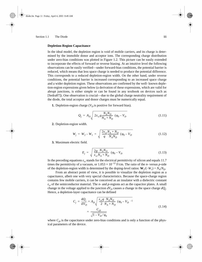
Depletion-Region Capacitance
In the ideal model, the depletion region is void of mobile carriers, and its charge is deter-mined by the immobile donor and acceptor ions. The corresponding charge distributionunder zero-bias conditions was plotted in Figure 1.2. This picture can be easily extendedto incorporate the effects of forward or reverse biasing. At an intuitive level the followingobservations can be easily verified—under forward-bias conditions, the potential barrier isreduced, which means that less space charge is needed to produce the potential difference.This corresponds to a reduced depletion-region width. On the other hand, under reverseconditions, the potential barrier is increased corresponding to an increased space chargeand a wider depletion region. These observations are confirmed by the well- known deple-tion-region expressions given below (a derivation of these expressions, which are valid forabrupt junctions, is either simple or can be found in any textbook on devices such as[Sedra87]). One observation is crucial—due to the global charge neutrality requirement ofthe diode, the total acceptor and donor charges must be numerically equal.
1. Depletion-region charge (VD is positive for forward bias).
(1.11)
2. Depletion-region width.
(1.12)
3. Maximum electric field.
(1.13)
In the preceding equations εsi stands for the electrical permittivity of silicon and equals 11.7times the permittivity of a vacuum, or 1.053 × 10⁻¹² F/cm. The ratio of the n- versus p-sideof the depletion-region width is determined by the doping-level ratios: W2/(−W1) = NA/ND.
From an abstract point of view, it is possible to visualize the depletion region as acapacitance, albeit one with very special characteristics. Because the space-charge regioncontains few mobile carriers, it can be conceived as an insulator with a dielectric constantεsi of the semiconductor material. The n- and p-regions act as the capacitor plates. A smallchange in the voltage applied to the junction dVD causes a change in the space charge dQj.Hence, a depletion-layer capacitance can be defined
(1.14)
where Cj0 is the capacitance under zero-bias conditions and is only a function of the phys-ical parameters of the device.
Qj AD 2εsiqNAND
NA ND+--------------------
φ0 VD–( )=
Wj W2 W1–2εsi
q---------
NA ND+NAND
-------------------- φ0 VD–( )= =
Ej2qεsi------
NAND
NA ND+--------------------
φ0 VD–( )=
Cj VDddQj AD
εsiq2
---------NAND
NA ND+--------------------
φ0 VD–( ) 1–==
Cj0
1 VD φ0⁄–-----------------------------=
diode.fm Page 11 Friday, April 4, 2003 8:49 AM

12 THE DIODE Chapter 1
(1.15)
Notice that the same capacitance value is obtained when using the standard parallel-platecapacitor equation Cj = εsi AD/Wj (with Wj given in Eq. (1.12)) Typically, the AD factor isomitted, and Cj and Cj0 are expressed as a capacitance/unit area.
The resulting junction capacitance is plotted in the function of the bias voltage inFigure 1.9 for a typical silicon diode found in MOS circuits. A strong nonlinear depen-dence can be observed. Note also that the capacitance decreases with an increasing reversebias: a reverse bias of 5 V reduces the capacitance by more than a factor of two.
Example 1.3 Junction Capacitance
Consider the following silicon junction diode: Cj0 = 0.5 fF/µm2, AD = 12 µm2 and φ0 = 0.64 V.A reverse bias of −5 V results in a junction capacitance of 0.17 fF/µm2, or, for the total diode,a capacitance of 2.02 fF.
Equation (1.14) is only valid under the condition that the pn-junction is an abruptjunction, where the transition from n to p material is instantaneous. This is often not thecase in actual integrated-circuit pn-junctions, where the transition from n to p material canbe gradual. In those cases, a linear distribution of the impurities across the junction is abetter approximation than the step function of the abrupt junction. An analysis of thelinearly-graded junction shows that the junction capacitance equation of Eq. (1.14) stillholds, but with a variation in order of the denominator. A more generic expression for thejunction capacitance can hence be provided,
(1.16)
Cj0 ADεsiq
2---------
NAND
NA ND+--------------------
φ01–=
Figure 1.9 Junction capacitance (in fF/µm2) as a function of the applied bias voltage.
-4.0 -2.0 0.0
VD (V)
0.0
0.5
1.0
1.5
2.0
Cj (
fF)
Abrupt junction
Linear junction
Cj0
m = 0.5
m = 0.33
CjCj0
1 VD φ0⁄–( )m---------------------------------=
diode.fm Page 12 Friday, April 4, 2003 8:49 AM
Section 1.1 The Diode 13
where m is called the grading coefficient and equals 1/2 for the abrupt junction and 1/3 forthe linear or graded junction. Both cases are illustrated in Figure 1.9.
The reader should be aware that the junction capacitance is actually a small-signalparameter whose value varies over bias points. In digital circuits, operating voltages tendto move rapidly over wide ranges. Under those circumstances, it is more attractive toreplace the voltage-dependent, nonlinear capacitance Cj by an equivalent, linear capaci-tance Ceq. Ceq is defined such that, for a given voltage swing from voltages Vhigh to Vlow,the same amount of charge is transferred as would be predicted by the nonlinear model
(1.17)
Combining Eq. (1.11) (extended to accommodate the grading coefficient m) and Eq.(1.17) yields the value of Keq.
(1.18)
Example 1.4 Average Junction Capacitance
The diode of Example 1.3 is switched between 0 and −5 V. Compute the average junctioncapacitance (m = 0.5).
For the defined voltage range and for φ0 = 0.64 V, Keq evaluates to 0.502. The averagecapacitance hence equals 0.25 fF/µm2.
Diffusion Capacitance
Under forward bias, the pn-junction exhibits a capacitive effect much larger than just thejunction capacitance. This extra capacitive effect is due to the excess minority carriercharge stored at the boundaries of the depletion region.
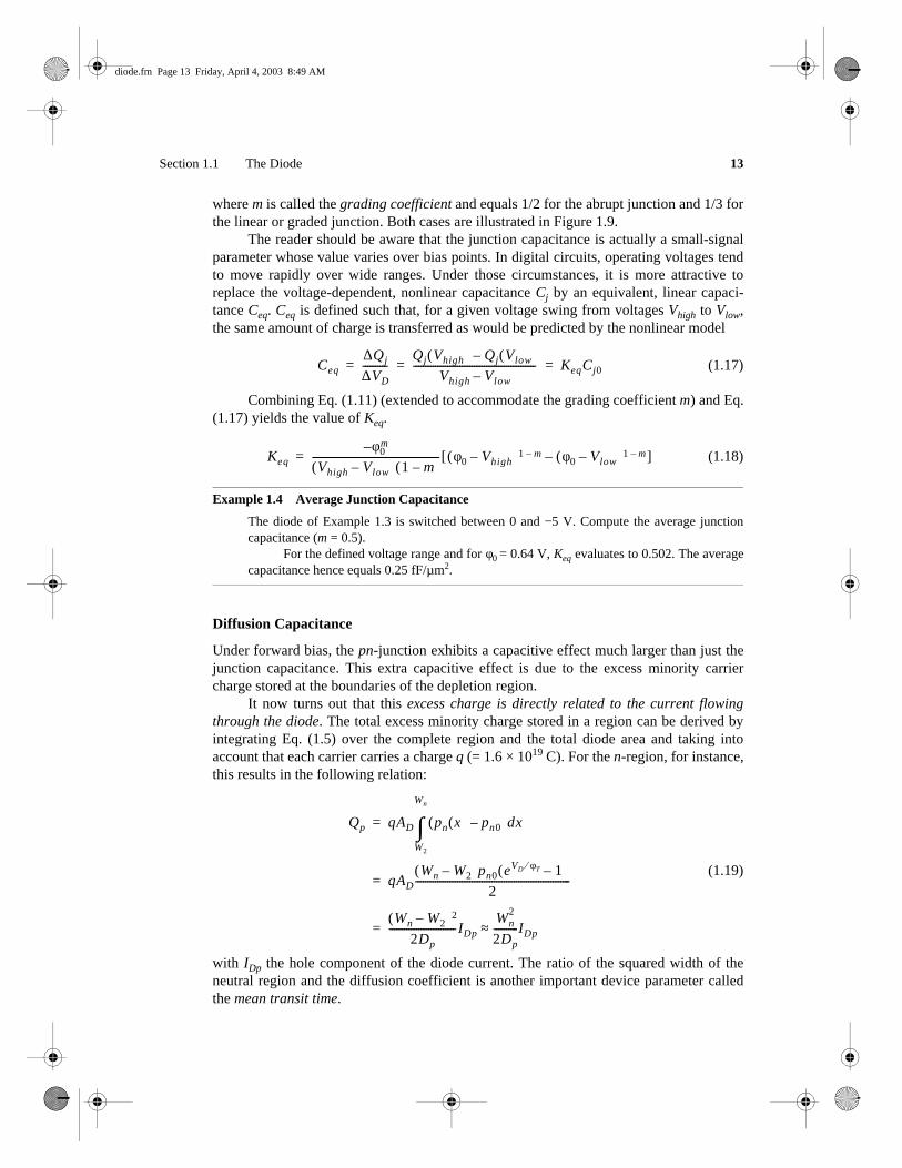
It now turns out that this excess charge is directly related to the current flowingthrough the diode. The total excess minority charge stored in a region can be derived byintegrating Eq. (1.5) over the complete region and the total diode area and taking intoaccount that each carrier carries a charge q (= 1.6 × 10¹⁹ C). For the n-region, for instance,this results in the following relation:
(1.19)
with IDp the hole component of the diode current. The ratio of the squared width of theneutral region and the diffusion coefficient is another important device parameter calledthe mean transit time.
Ceq∆Qj
∆VD----------
Qj Vhigh( ) Qj Vlow( )–Vhigh Vlow–
-------------------------------------------------- KeqCj0= = =
Keqφ0
m–Vhigh Vlow–( ) 1 m–( )
---------------------------------------------------- φ0 Vhigh–( )1 m– φ0 Vlow–( )1 m––[ ]=
Qp qAD pn x( ) pn0–( )dx
W2
Wn
∫=
qADWn W2–( )pn0 eVD φT⁄ 1 )–(
2---------------------------------------------------------------=
Wn W2–( )2
2Dp---------------------------IDp
Wn2
2Dp----------IDp≈=
diode.fm Page 13 Friday, April 4, 2003 8:49 AM

14 THE DIODE Chapter 1
(1.20)
The total diode current can now be expressed as a function of the excess minority carriercharge
(1.21)
This equation simply states that, in the steady state, the current ID is inversely pro-portional to the time it takes a carrier to transport from the junction to the metallic contact.
Example 1.5 Mean Transit Times
For the diode of Problem 1.1, the mean transit times evaluate to the following values:
τTp = (5 µm − 0.15 µm)2/ (2 × 10 cm2/sec) = 11.7 nsec
τTn = (0.7 µm − 0.03 µm)2/ (2 × 25 cm2/sec) = 0.09 nsec
Similar expressions can be derived for the long-base diode. In that case, the transittime is replaced by the excess minority carrier lifetime parameter, which indicates themean time it takes for an injected minority carrier to recombine with a majority carrier.
(1.22)
In silicon, typical values of Lp and Ln range from 1 to 100 µm, and the corresponding val-ues of the lifetime are in the range of 1 to 10,000 nsec.
Under transient conditions, a change in current translates into a change in the excessminority carrier charge. In correspondence with the approach used for the depletionregion, we model the effect of this charge by an equivalent capacitance called the diffusioncapacitance Cd. The value of Cd
is easily derived
(1.23)
which shows a linear dependence upon ID (as could be expected). For reverse bias, it is fairto assume that Cd is ignorable. Observe, once again, that Cd is a small-signal capacitanceand is only valid around a given bias voltage.
Similar to the junction capacitance, an average diffusion capacitance can be definedfor a voltage range of interest.
τTpWn
2
2Dp---------- sec=
and
τTnWp
2
2Dn---------- sec=
IDQp
τTp-------
Qn
τTn-------+
QD
τT-------= =
τp Lp2 Dp⁄ sec=
and
τn Ln2 Dn⁄ sec=
Cd VDddQD τT VDd
dID τTID
φT----------≈= =
diode.fm Page 14 Friday, April 4, 2003 8:49 AM

Section 1.1 The Diode 15
(1.24)
Example 1.6 Diffusion Capacitance
For IS = 0.5 × 10⁻¹⁶A, τT = 1 nsec, and φT = 26 mV, Cd evaluates to a capacitance of 6.5 pF fora forward bias of 0.75V.
Diode Switching Time: A Case Study
The presented models can now be employed to determine the time it takes to switch adiode between two different states. Consider the circuit of Figure 1.10a. Before time 0, thevoltage source Vsrc provides a strong forward bias for the diode (V1 >> VD,on). At time t =0, the voltage source switches to a negative voltage, such that the diode goes into reversebias. At time t = T, the voltage source is reversed again, turning on the diode. We simplifythe analysis by replacing the voltage source and its resistance by the Norton equivalentcircuit (Figure 1.10b). It is assumed that the source resistance Rsrc is large enough so thatvirtually all current flows through the diode in forward-bias conditions.
To determine how fast the circuit will move to a new steady state, we analyze theequivalent circuit of Figure 1.10c, where the diode is replaced by a nonlinear currentsource (representing the ideal diode equation) and two capacitances, representing the spacecharge (Cj) and the excess minority carrier charge (Cd), respectively. Once again, observethat Cj and Cd are small signal-capacitances. To be applicable to large-signal analysis,averaged capacitance values must be used. The model for the reverse-bias operation modeis obtained by simply eliminating the current source ID and the diffusion capacitance CD.
CD∆QD
∆VD----------- τT
ID Vhigh( ) ID Vlow( )–( )Vhigh Vlow–
------------------------------------------------------ φTCd high( ) Cd low( )–( )
Vhigh Vlow–----------------------------------------------= = =
IDCdRsrc
Isrc
(b) Norton equivalent circuit
RsrcIsrc
Cj
VDVD
(c) Equivalent circuit for transient analysis
Figure 1.10 Diode switching time.
Vsrc
t = 0
V1
V2
VD
Rsrc
t = T
ID
t = 0
I1
I2 t = T
(a) Diode switched by voltage source
diode.fm Page 15 Friday, April 4, 2003 8:49 AM

16 THE DIODE Chapter 1
Deriving the transient response of this network seems simple, as it requires the“mere” solution of the following differential equation:
o (1.25)
Unfortunately, this equation is heavily nonlinear again, and finding an analyticalsolution is a daunting task, which is easily solved by a computer but hard to performmanually. Observe that Cd and Cj are nonlinear functions of VD as well. Some simplifica-tions are hence at hand. A glimpse of how to tackle this is offered by an inspection of asimulated response, shown in Figure 1.11.
The turn-off transient, for instance, clearly displays two operation intervals:
1. Initially, the reverse current I2 is used to remove the excess minority carrier chargefrom the neutral regions. During that time, the diode remains on, and the voltageover the diode is approximately constant. This is easily understood: a linear drop involtage requires an exponential drop in current (and equivalently in excess charge).The constant voltage means that the space charge remains approximately constant aswell. The effect of Cj can be ignored during this interval.
2. Once the diode has been turned off (ID ≈ 0), the circuit evolves towards steady state.While building a reverse bias over the diode, the space charge changes. In thisregion, the junction capacitance Cj dominates the performance.
The reader should be aware that the partitioning of the transient into two intervals is some-what artificial and that both intervals overlap. For instance, in the later phases of the diodeturn-off, not all excess charge is removed, yet the voltage over the diode starts to drop,changing the space charge. It is fair to assume that the impact of the space charge is domi-nant at that time, as the excess charge has been reduced to minuscule amounts (once again,this is a consequence of the exponential relationship between excess charge and diodevoltage). The assumption is therefore very reasonable.
Based on these observations, we can derive the duration of both intervals. We firstaddress the turn-off transient.
Isrc ID t( ) Cd Cj+( )td
dVD+ IS eVD t( ) φT⁄ 1–( ) Cd Cj+( )td
dVD+= =
Figure 1.11 Simulated transient response of diode. Time
VD
ON OFF ON
Space charge
Excess charge
diode.fm Page 16 Friday, April 4, 2003 8:49 AM
Section 1.1 The Diode 17
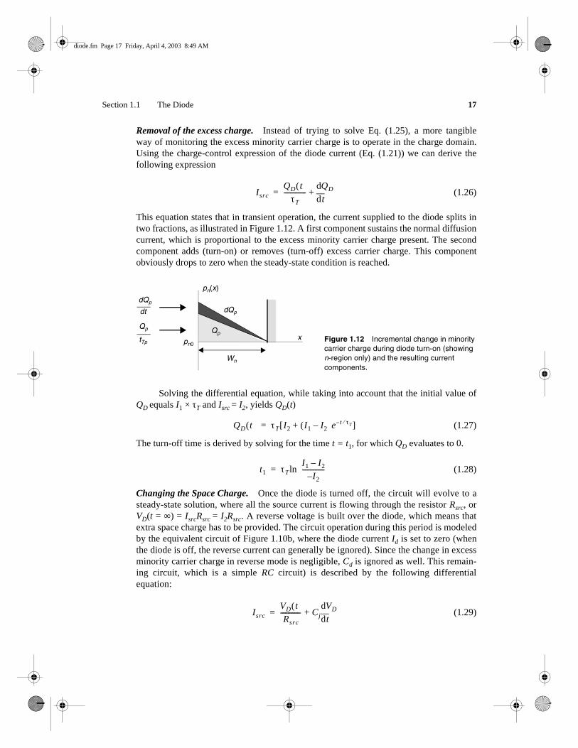
Removal of the excess charge. Instead of trying to solve Eq. (1.25), a more tangibleway of monitoring the excess minority carrier charge is to operate in the charge domain.Using the charge-control expression of the diode current (Eq. (1.21)) we can derive thefollowing expression
(1.26)
This equation states that in transient operation, the current supplied to the diode splits intwo fractions, as illustrated in Figure 1.12. A first component sustains the normal diffusioncurrent, which is proportional to the excess minority carrier charge present. The secondcomponent adds (turn-on) or removes (turn-off) excess carrier charge. This componentobviously drops to zero when the steady-state condition is reached.
Solving the differential equation, while taking into account that the initial value ofQD equals I1 × τT and Isrc = I2, yields QD(t)
(1.27)
The turn-off time is derived by solving for the time t = t1, for which QD evaluates to 0.
(1.28)
Changing the Space Charge. Once the diode is turned off, the circuit will evolve to asteady-state solution, where all the source current is flowing through the resistor Rsrc, orVD(t = ∞) = IsrcRsrc = I2Rsrc. A reverse voltage is built over the diode, which means thatextra space charge has to be provided. The circuit operation during this period is modeledby the equivalent circuit of Figure 1.10b, where the diode current Id is set to zero (whenthe diode is off, the reverse current can generally be ignored). Since the change in excessminority carrier charge in reverse mode is negligible, Cd is ignored as well. This remain-ing circuit, which is a simple RC circuit) is described by the following differentialequation:
(1.29)
IsrcQD t( )
τT--------------
tddQD+=
xpn0
Wn
pn(x)
Qp
dQp
Qp
tTp
dQp
dt
Figure 1.12 Incremental change in minority carrier charge during diode turn-on (showing n-region only) and the resulting current components.
QD t( ) τT I2 I1 I2–( )e t τT⁄–+[ ]=
t1 τTlnI1 I2–
I2–--------------
=
IsrcVD t( )Rsrc
------------- Cj tddVD+=
diode.fm Page 17 Friday, April 4, 2003 8:49 AM

18 THE DIODE Chapter 1
where Cj is the average junction capacitance over the voltage region of interest. Assumingthat the value of VD at time t = t1 equals 0, the solution of this equation is the well-knownexponential expression2
(1.30)
The diode voltage reaches its final value in an asymptotic fashion. For such a wave-form, the 90% point is often used to determine the end of the transition (as the 100% pointwould take infinitely long). It is easily determined that this 90% point is reached after 2.3time-constants RsrcCj.
Turn-on Transient. Similar considerations hold for the turn-on transient, as is illus-trated in Figure 1.11. Before the diode can be turned on, it is necessary to change the spacecharge first. The transient waveform for the diode voltage is easily derived (using a similarapproach as above, and assuming that the transient starts at time t = 0):
(1.31)
Solving this equation for VD = 0 (the time the diode starts to turn on) yields
(1.32)
The build-up of the space-charge is still described by the differential equation (1.26). Withthe proper initial condition (QD(t = t3) = 0), solving this equation shows that the excesscharge increases in an exponential fashion and asymptotically approaches its final value
(1.33)
It takes approximately 2.2 time constants τT for QD to reach 90% of its final value.The procedures used above are representative of the analysis and derivation tech-
niques to be used in the chapters to come—using a number of approximations and linear-izations, a simple, tractable model is constructed of a complex, nonlinear circuit. Althoughinaccurate, this model fosters insight into the circuit operation and identifies the dominantparameters. The first-order solution obtained from this analysis can then be further opti-mized, or fine-tuned, using computer-aided tools.
Example 1.7 Diode Transient Response
Consider the diode circuit of Figure 1.10 for the following parameters: Rsrc = 50 kΩ,I1 = 1 mA, I2 = −0.1 mA. The following parameters are used for the diode: IS = 2 × 10⁻¹⁶A,Cj0 = 0.2 pF, τT = 5 nsec, and φ0 = 0.65.
2 One can argue that the junction capacitance starts to dominate at the point where VD = φ0 and that thisshould be the starting point of the second interval. Adopting this assumption does not affect the final result in amajor way.
VD t( ) I2Rsrc 1 et t1–
RsrcCj---------------–
–
=
VD t( ) Rsrc I1 I2 I1–( )et
RsrcCj---------------–
–
=
t3 RsrcCjI1 I2–
I1--------------
ln=
QD t( ) I1τT 1 et t3–
τT-----------–
–=
diode.fm Page 18 Friday, April 4, 2003 8:49 AM

Section 1.1 The Diode 19
The steady-state voltages over the diode are easily derived,
VD (diode on) = φT ln (ID/IS) = 0.75 V
VD (diode off) = I2Rsrc = −0.1 mA × 50 kΩ = −5 V.
Using the expressions derived above, we can further estimate the lengths of the variousintervals in the turn-off and turn-on transients:
Finding an approximation of (t2 − t1) requires first of all a value for the average junc-tion capacitance Cj, which can be obtained with the aid of Eq. (1.18),
assuming a voltage swing from 0 to −5V. Using this information we can easily derive the90% transition point
This yields a total turn-off time of 23.2 nsec. For the turn-on, we obtain the followingdelays
and
which translates into a turn-on time of approximately 11.5 nsec. The faster response is due tolarger current (1 mA) available for turning on the device (versus the 0.1 mA for turn-off).
A SPICE simulation of the same circuit produces a transient response similar to the oneshown in Figure 1.11 and the following numerical results: t1 (0 voltage crossing) = 13.2 nsec,t2 (−4.5 V or 90% of the final value) = 23.6 nsec and t3 (0 voltage crossing) = 0.57 nsec.Determining the correct value of t4 is hard as there no direct way to derive the value of QD(and its 90% point) from the simulation results.
The obtained numbers are in perfect agreement with the simulated ones. The closenessof the match is, however, partially due to good luck. While building the estimation model, wemade a number of approximations and simplifications, which obviously cause deviationsfrom the actual result. The art of approximation is to keep the errors within reasonablebounds.
1.1.4 The Actual Diode—Secondary Effects
In practice, the diode current is less than what is predicted by the ideal diode equation. Notall applied bias voltage appears directly across the junction, as there is always some volt-age drop over the neutral regions. Fortunately, the resistivity of the neutral zones is gener-ally small (between 1 and 100 Ω, depending upon the doping levels) and the voltage drop
t1 5 nsec ln1 0.1+0.1
----------------× 12 nsec= =
Cj KeqCj0 0.51 0.2× 0.102 pF= = =
t2 t1– 2.2 50kΩ 0.102pF×× 11.2 nsec= =
t3 50 kΩ 0.102 pF·× ln1 0.1+1
----------------× 0.49 nsec= =
t4 t3– 2.2 5 nsec× 11 nsec= =
diode.fm Page 19 Friday, April 4, 2003 8:49 AM

20 THE DIODE Chapter 1
only becomes significant for large currents (>1 mA). This effect can be modeled by add-ing a resistor in series with the n- and p-region diode contacts.
In the discussion above, it was assumed that under sufficient reverse bias, thereverse current reaches a constant value, which is essentially zero. When the reverse biasexceeds a certain level, called the breakdown voltage, the reverse current shows a dra-matic increase as shown in Figure 1.13. In the diodes found in typical MOS and bipolar
processes, this increase is caused by the avalanche breakdown. The increasing reversebias causes the magnitude of the electrical field across the junction to increase. Conse-quently, carriers crossing the depletion region are accelerated to high velocity. At a criticalfield Ecrit , the carriers reach a high enough energy level that electron-hole pairs are createdon collision with immobile silicon atoms. These carriers create, in turn, more carriersbefore leaving the depletion region. The value of Ecri t is approximately 2 × 10⁵ V/cm forimpurity concentrations of the order of 1016 cm−3. While avalanche breakdown in itself isnot destructive and its effects disappear after the reverse bias is removed, maintaining adiode for a long time in avalanche conditions is not recommended as the high current lev-els (and the associated power dissipation) might cause permanent damage to the structure.Observe that avalanche breakdown is not the only breakdown mechanism encountered indiodes. For highly doped diodes, another mechanism, called Zener breakdown, can occur.Discussion of this phenomenon is beyond the scope of this text.
Finally, it is worth mentioning that the diode current is affected by the operatingtemperature in a dual way:
1. The thermal voltage φT, which appears in the exponent of the current equation, islinearly dependent upon the temperature. An increase in φT causes the current todrop.
2. The saturation current IS is also temperature-dependent, as the thermal equilibriumcarrier concentrations increase with increasing temperature. Theoretically, the satu-ration current approximately doubles every 5 °C. Experimentally, the reverse cur-rent has been measured to double every 8 °C.
This dual dependence has a significant impact on the operation of a digital circuit. First ofall, current levels (and hence power consumption) can increase substantially. For instance,for a forward bias of 0.7 V at 300 K, the current increases approximately 6%/°C, and dou-
Figure 1.13 I-V characteristic of junction diode, showing breakdown under reverse-bias conditions (Breakdown voltage = 20 V).
–25.0 –15.0 –5.0 5.0
VD (V)
–0.1
I D (A
)
0.1
0
0
diode.fm Page 20 Friday, April 4, 2003 8:49 AM

Section 1.1 The Diode 21
bles every 12 °C. Secondly, integrated circuits rely heavily on reverse-biased diodes asisolators. Increasing the temperature causes the leakage current to increase and decreasesthe isolation quality.
1.1.5 The SPICE Diode Model
In the preceding sections, we have presented a model for manual analysis of a diode cir-cuit. For more complex circuits, or when a more accurate modeling of the diode that takesinto account second-order effects is required, manual circuit evaluation becomes intracta-ble, and computer-aided simulation is necessary. While different circuit simulators havebeen developed over the last decades, the SPICE program, developed at the University ofCalifornia at Berkeley, is definitely the most successful [Nagel75]. Simulating an inte-grated circuit containing active devices requires a mathematical model for those devices(which is called the SPICE model in the rest of the text). The accuracy of the simulationdepends directly upon the quality of this model. For instance, one cannot expect to see theresult of a second-order effect in the simulation if this effect is not present in the devicemodel. Creating accurate and computation-efficient SPICE models has been a long pro-cess and is by no means finished. Every major semiconductor company has developedtheir own proprietary models, which it claims have either better accuracy or computationalefficiency and robustness.
The standard SPICE model for a diode is simple, as shown in Figure 1.14. Thesteady-state characteristic of the diode is modeled by the nonlinear current source ID,which is a modified version of the ideal diode equation
(1.34)
The extra parameter n is called the emission coefficient. It equals 1 for most com-mon diodes but can be somewhat higher than 1 for others. The resistor Rs models theseries resistance contributed by the neutral regions on both sides of the junction. Forhigher current levels, this resistance causes the internal diode VD to differ from the exter-nally applied voltage, hence causing the current to be lower than what would be expectedfrom the ideal diode equation.
Figure 1.14 SPICE diode model.
ID
RS
CD
+
–
VD
ID IS eVD nφT⁄ 1–( )=
diode.fm Page 21 Friday, April 4, 2003 8:49 AM
22 THE DIODE Chapter 1
The dynamic behavior of the diode is modeled by the nonlinear capacitance CD,which combines the two different charge-storage effects in the diode: the excess minoritycarrier charge and the space charge.
(1.35)
We can verify that this equation is, aside from the introduction of the emission coefficient,nothing else than a combination of Eq. (1.23) and Eq. (1.16). The parameter τT is calledthe transit time and represents, depending upon the diode type, the excess minority carrierlifetime (τn, τp) for long-base diodes, or the mean transit time τT for short-base diodes.
A listing of the parameters used in the diode model is given in Table 1.1. Besides theparameter name, symbol, and SPICE name, the table contains also the default value usedby SPICE in case the parameter is left undefined. Observe that this table is by no meanscomplete. Other parameters are available to govern second-order effects such as break-down, high-level injection, and noise. To be concise, we chose to limit the listing to theparameters of direct interest to this text. For a complete description of the device models(as well as the usage of SPICE), we refer to the numerous textbooks devoted to SPICE(e.g., [Banhzaf92], [Thorpe92]).
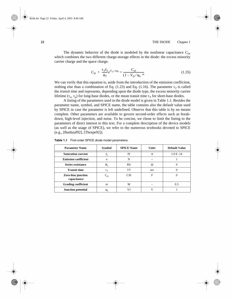
Table 1.1 First-order SPICE diode model parameters.
Parameter Name Symbol SPICE Name Units Default Value
Saturation current IS IS A 1.0 E−14
Emission coefficient n N – 1
Series resistance RS RS Ω 0
Transit time τT TT sec 0
Zero-bias junction capacitance
Cj0 CJ0 F 0
Grading coefficient m M – 0.5
Junction potential φ0 VJ V 1
CDτTIS
φT---------eVD nφT⁄ Cj0
1 VD φ0⁄–( )m---------------------------------+=
diode.fm Page 22 Friday, April 4, 2003 8:49 AM