rial Circuits
57
Combinational Logic Implementation: Multi-Level Networks
-
Upload
mod-ali-radi -
Category
Documents
-
view
226 -
download
0
Transcript of rial Circuits
8/2/2019 rial Circuits
http://slidepdf.com/reader/full/rial-circuits 1/57
Combinational Logic Implementation: Multi-Level Networks
8/2/2019 rial Circuits
http://slidepdf.com/reader/full/rial-circuits 2/57
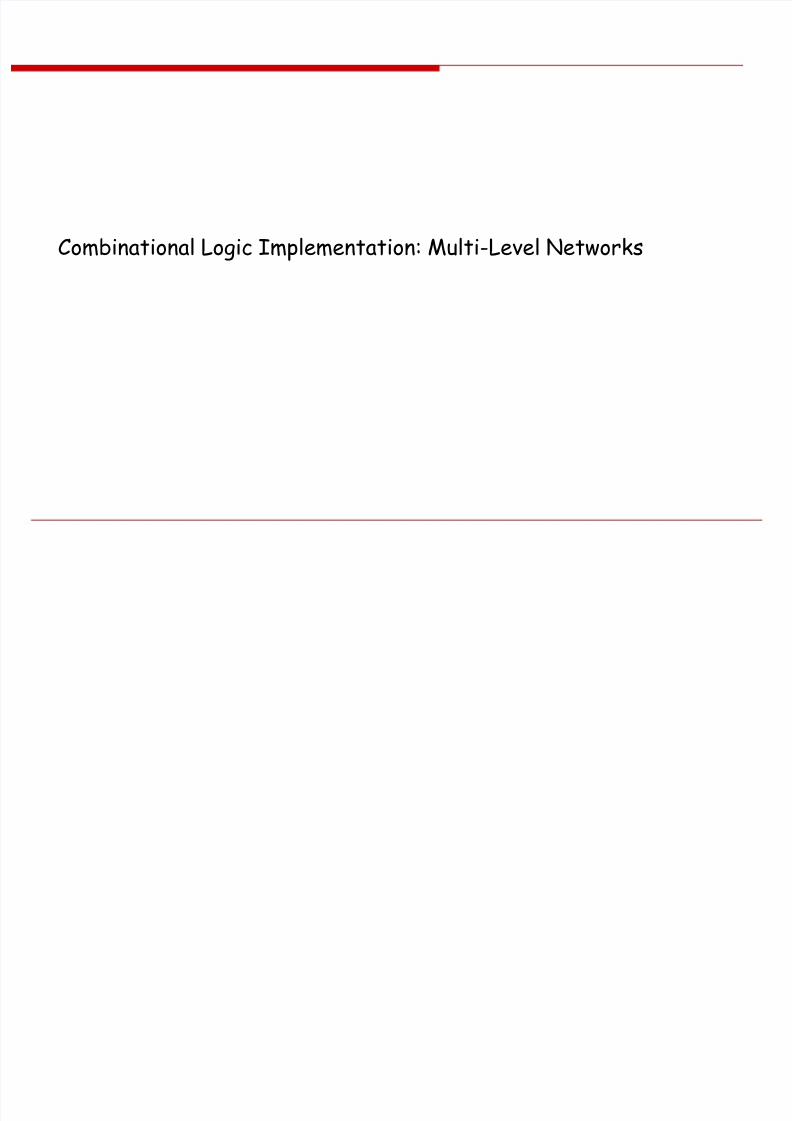
Implementations of Two-level Logic
Sum-of-products
AND gates to form product terms(minterms)
OR gate to form sum
Product-of-sums
OR gates to form sum terms(maxterms)
AND gates to form product

8/2/2019 rial Circuits
http://slidepdf.com/reader/full/rial-circuits 3/57
Two-level Logic using NAND Gates
Replace minterm AND gates with NAND gates
Place compensating inversion at inputs of OR gate
8/2/2019 rial Circuits
http://slidepdf.com/reader/full/rial-circuits 4/57
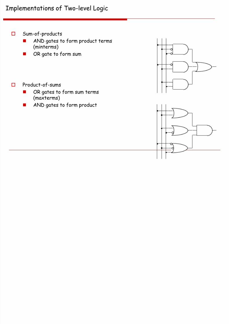
Two-level Logic using NAND Gates (cont’d)
OR gate with inverted inputs is a NAND gate
de Morgan's: A' + B' = (A • B)' Two-level NAND-NAND network
Inverted inputs are not counted
In a typical circuit, inversion is done once and signal distributed

8/2/2019 rial Circuits
http://slidepdf.com/reader/full/rial-circuits 5/57
Two-level Logic using NOR Gates
Replace maxterm OR gates with NOR gates
Place compensating inversion at inputs of AND gate
8/2/2019 rial Circuits
http://slidepdf.com/reader/full/rial-circuits 6/57
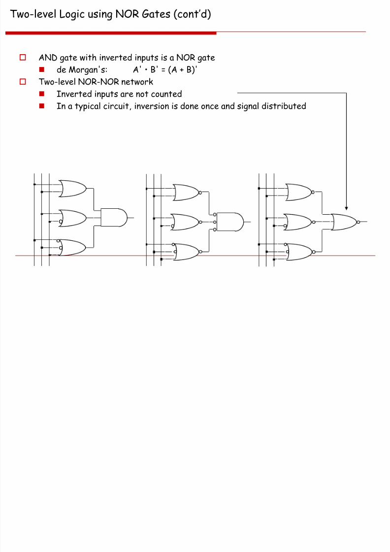
Two-level Logic using NOR Gates (cont’d)
AND gate with inverted inputs is a NOR gate
de Morgan's: A' • B' = (A + B)' Two-level NOR-NOR network
Inverted inputs are not counted
In a typical circuit, inversion is done once and signal distributed

8/2/2019 rial Circuits
http://slidepdf.com/reader/full/rial-circuits 7/57
OR
NAND NAND
OR AND
NOR NOR
AND
Two-level Logic using NAND and NOR Gates
NAND-NAND and NOR-NOR networks
de Morgan's law: (A + B)' = A' • B'(A • B)' = A' + B'
written differently: A + B = (A' • B')’(A • B) = (A' + B')'
In other words –– OR is the same as NAND with complemented inputs AND is the same as NOR with complemented inputs
NAND is the same as OR with complemented inputs NOR is the same as AND with complemented inputs

8/2/2019 rial Circuits
http://slidepdf.com/reader/full/rial-circuits 8/57
A
B
C
D
Z
A
B
C
D
Z
NAND
NAND
NAND
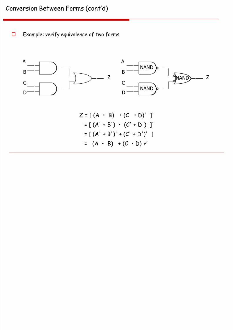
Conversion Between Forms
Convert from networks of ANDs and ORs to networks of NANDs and NORs
Introduce appropriate inversions ("bubbles") Each introduced "bubble" must be matched by a corresponding "bubble"
Conservation of inversions
Do not alter logic function
Example: AND/OR to NAND/NAND
8/2/2019 rial Circuits
http://slidepdf.com/reader/full/rial-circuits 9/57
Z = [ (A • B)' • (C • D)' ]'
= [ (A' + B') • (C' + D') ]'
= [ (A' + B')' + (C' + D')' ]
= (A • B) + (C • D)
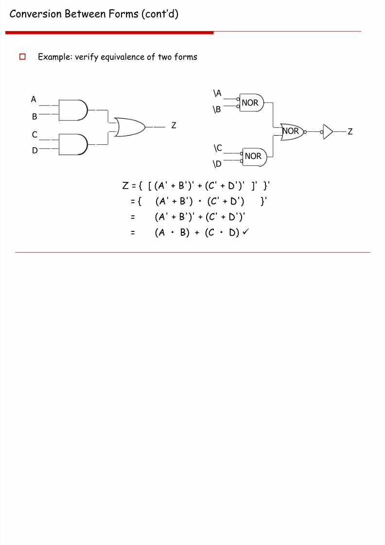
Conversion Between Forms (cont’d)
Example: verify equivalence of two forms
A
B
C
D
Z
A
B
C
D
Z
NAND
NAND
NAND
8/2/2019 rial Circuits
http://slidepdf.com/reader/full/rial-circuits 10/57
Z = { [ (A' + B')' + (C' + D')' ]' }'
= { (A' + B') • (C' + D') }'
= (A' + B')' + (C' + D')'
= (A • B) + (C • D)
Conversion Between Forms (cont’d)
Example: verify equivalence of two forms
A
B
C
D
Z
NOR
NOR
NOR
\A
\B
\C
\D
Z
8/2/2019 rial Circuits
http://slidepdf.com/reader/full/rial-circuits 11/57
A BC
DE
FG
X
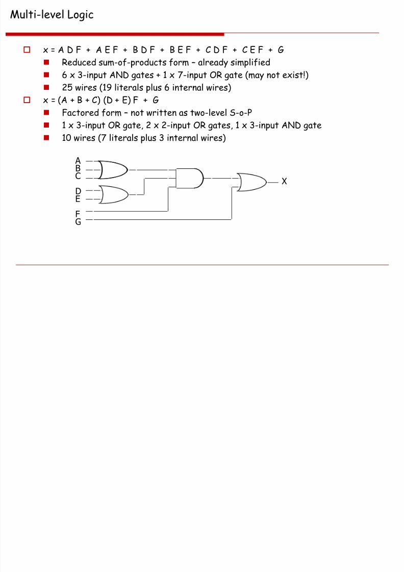
Multi-level Logic
x = A D F + A E F + B D F + B E F + C D F + C E F + G
Reduced sum-of-products form – already simplified
6 x 3-input AND gates + 1 x 7-input OR gate (may not exist!)
25 wires (19 literals plus 6 internal wires)
x = (A + B + C) (D + E) F + G
Factored form – not written as two-level S-o-P
1 x 3-input OR gate, 2 x 2-input OR gates, 1 x 3-input AND gate
10 wires (7 literals plus 3 internal wires)
8/2/2019 rial Circuits
http://slidepdf.com/reader/full/rial-circuits 12/57
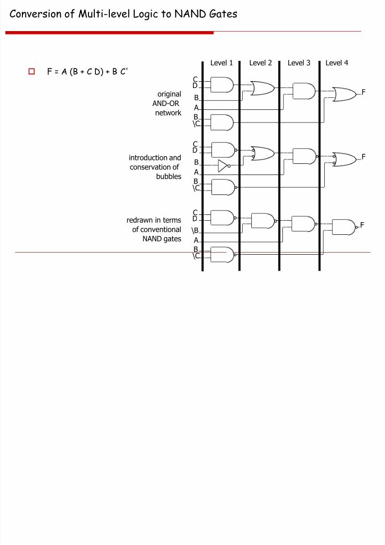
Level 1 Level 2 Level 3 Level 4
original
AND-OR
network A
CD
B
B\C
F
introduction and
conservation of
bubblesA
CD
B
B\C
F
redrawn in terms
of conventional
NAND gates A
CD
\B
B\C
F
Conversion of Multi-level Logic to NAND Gates
F = A (B + C D) + B C'
8/2/2019 rial Circuits
http://slidepdf.com/reader/full/rial-circuits 13/57
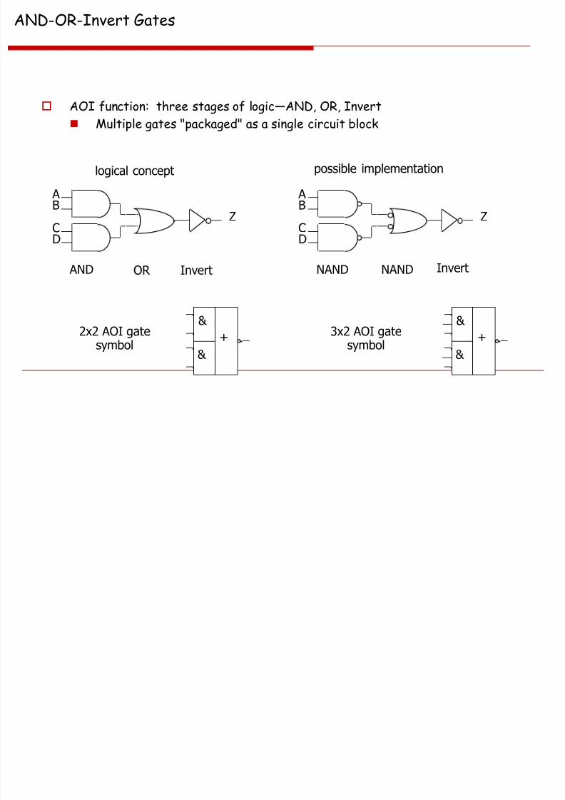
&
&
+2x2 AOI gatesymbol
&
&
+3x2 AOI gatesymbol
NAND NAND Invert
possible implementation
A B
CD
Z
AND OR Invert
logical concept
A B
CD
Z
AND-OR-Invert Gates
AOI function: three stages of logic—AND, OR, Invert
Multiple gates "packaged" as a single circuit block

8/2/2019 rial Circuits
http://slidepdf.com/reader/full/rial-circuits 14/57
14
Combinational Logic: Analysis and Design

8/2/2019 rial Circuits
http://slidepdf.com/reader/full/rial-circuits 15/57
15
Combinational Circuits
consists of logic gates with outputs that are
determined entirely by the present value of the inputs(no memory) Combinatorial circuits might be 2-level logic (SOP,POS) or
multi-level
o1
o2
om
i1i2i3 Comb. Logic
Two important procedure
Analysis – Given circuit schematic, explain itsbehavior
Design – Given the specifications, build it

8/2/2019 rial Circuits
http://slidepdf.com/reader/full/rial-circuits 16/57
16
Analysis Procedure
1. Label all logic gate outputs and primary inputs
2. Starting from primary inputs, represent outputs in terms of their input variables
3. Repeat 2, till you reach output
4. Represent primary output(s) in terms of primary inputs
F2 = AB +AC +BCT1 = A +B +C
T2 = ABC
T3 = F2’T1
F1 = T2 +T3
Simplify the F 1
8/2/2019 rial Circuits
http://slidepdf.com/reader/full/rial-circuits 17/57
17
Design Procedure
1. From Specifications, determine the required number of inputs
and outputs
2. Assign a variable to each input and output
3. Derive a truth Table that defines the required relationship
between inputs and outputs
4. Perform logic minimization
5. Draw the logic diagram
8/2/2019 rial Circuits
http://slidepdf.com/reader/full/rial-circuits 18/57
18
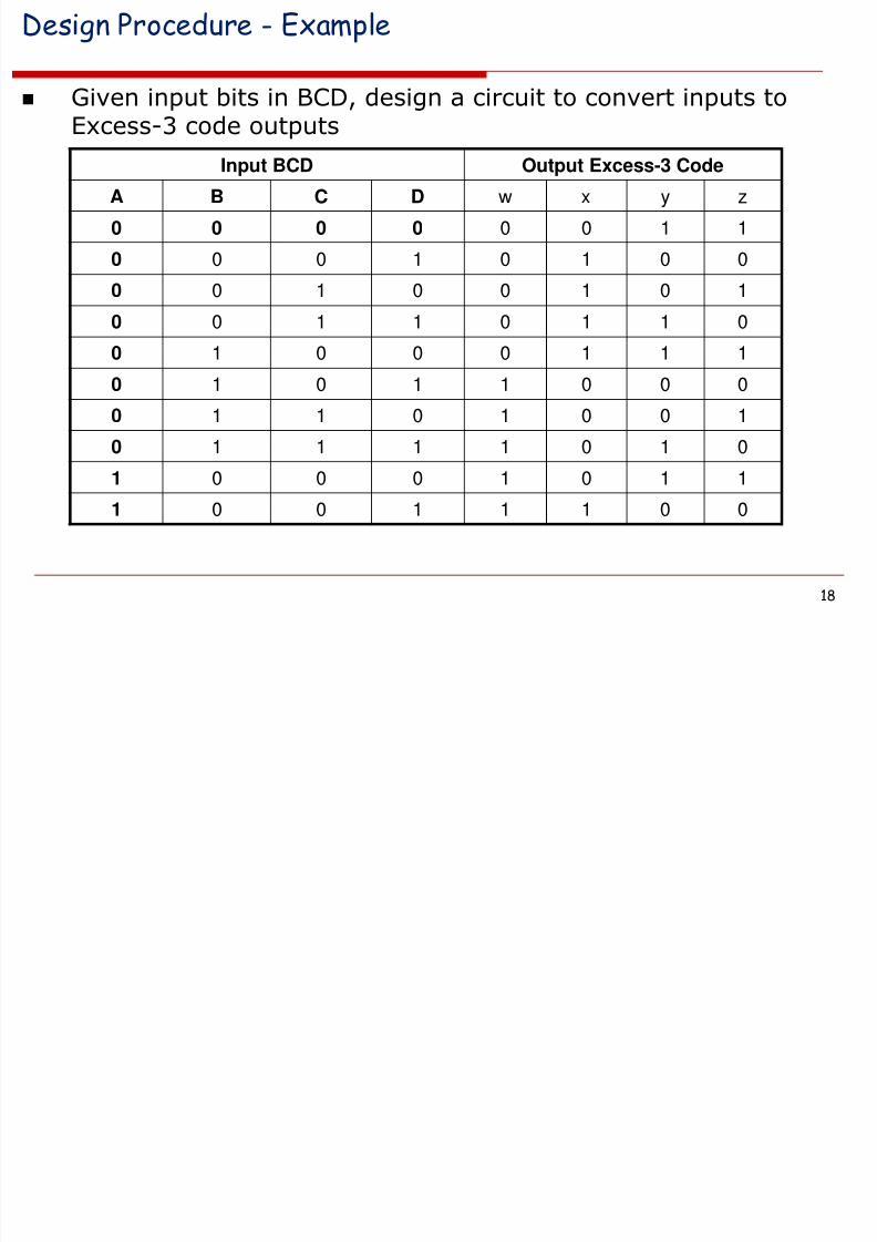
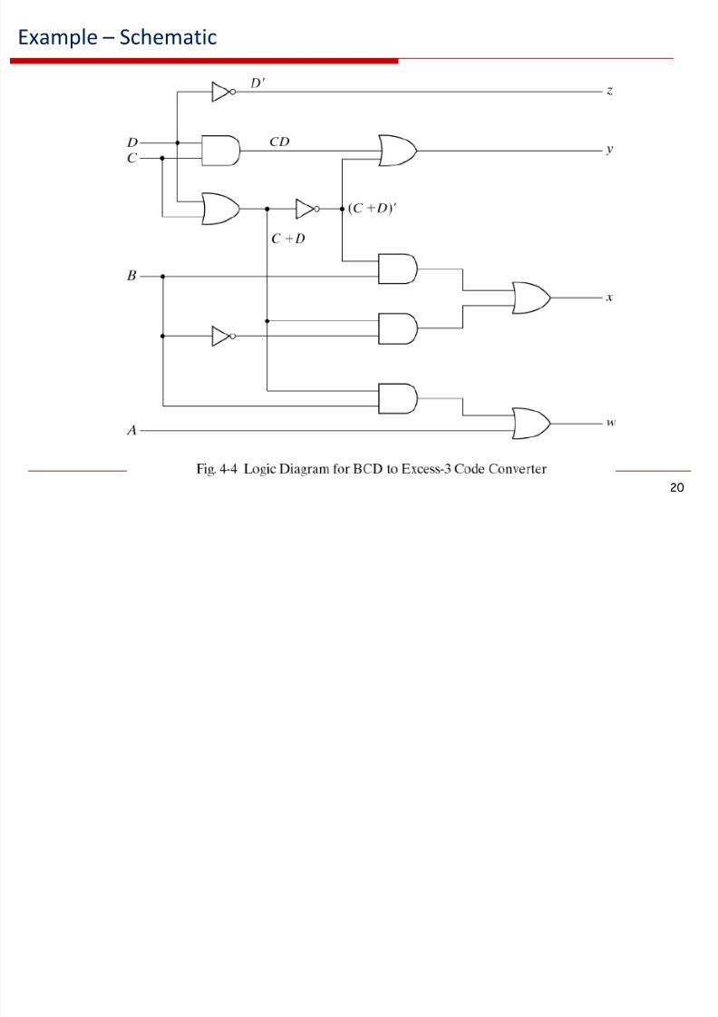
Design Procedure - Example
Given input bits in BCD, design a circuit to convert inputs toExcess-3 code outputs
Input BCD Output Excess-3 Code
A B C D w x y z
0 0 0 0 0 0 1 1
0 0 0 1 0 1 0 0
0 0 1 0 0 1 0 1
0 0 1 1 0 1 1 0
0 1 0 0 0 1 1 1
0 1 0 1 1 0 0 0
0 1 1 0 1 0 0 1
0 1 1 1 1 0 1 01 0 0 0 1 0 1 1
1 0 0 1 1 1 0 0
E l

8/2/2019 rial Circuits
http://slidepdf.com/reader/full/rial-circuits 19/57
19
Example – K maps
z = D’
y = CD +C’D’
= CD + (C +D)’
x = B’C +B’D +BC’D’
= B’(C +D) +B(C+D)’
w = A +BC +BD
= A +B(C+D)
8/2/2019 rial Circuits
http://slidepdf.com/reader/full/rial-circuits 20/57
20
Example – Schematic
8/2/2019 rial Circuits
http://slidepdf.com/reader/full/rial-circuits 21/57
21
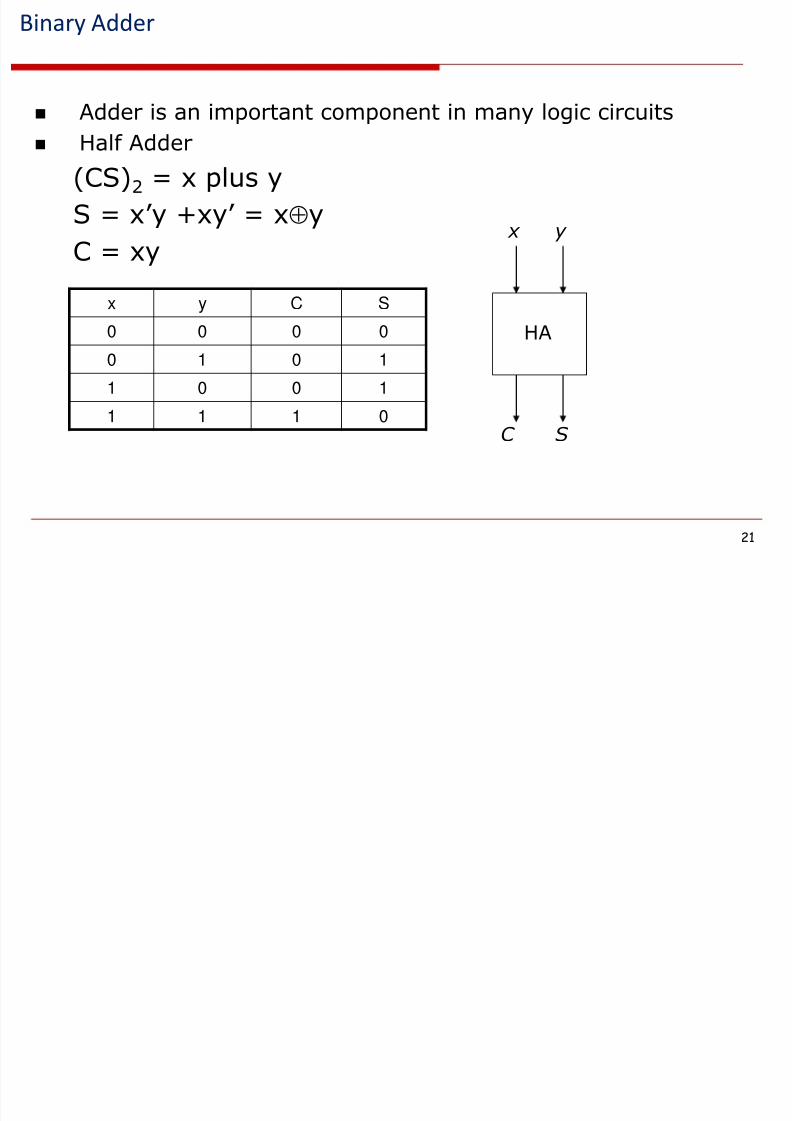
Binary Adder
Adder is an important component in many logic circuits
Half Adder
(CS)2 = x plus y
S = x’y +xy’ = xy
C = xy
x y C S
0 0 0 0
0 1 0 1
1 0 0 1
1 1 1 0
x y
C S
HA
ll dd
8/2/2019 rial Circuits
http://slidepdf.com/reader/full/rial-circuits 22/57
22
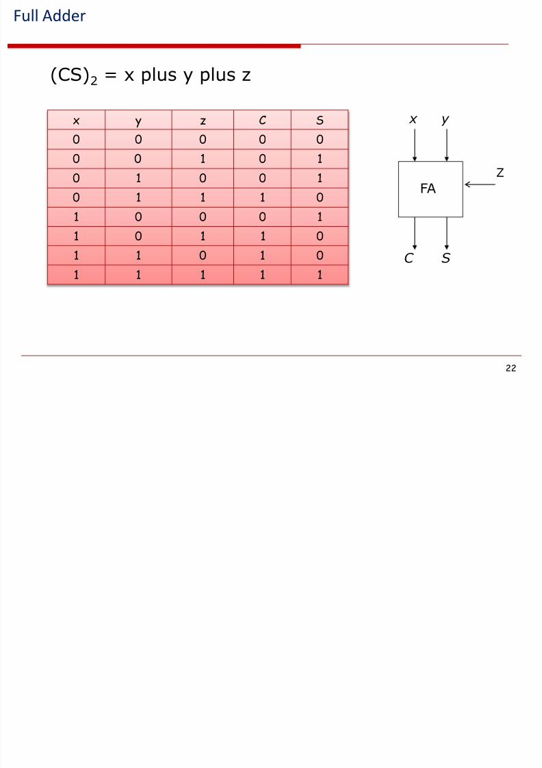
Full Adder
x y z C S
0 0 0 0 0
0 0 1 0 1
0 1 0 0 1
0 1 1 1 0
1 0 0 0 1
1 0 1 1 0
1 1 0 1 0
1 1 1 1 1
(CS)2 = x plus y plus z
x y
C S
FA
Z

8/2/2019 rial Circuits
http://slidepdf.com/reader/full/rial-circuits 23/57
23
Full Adder – K Maps & Schematics
0 1
0100
01
0
1
yz
x
0
1
1
0
11 10
S
x
x
y
y
z
z
x´
y
x
x
x´
y´
y´
y
z
z´
z´
0 0
0100
10
0
1
yz
x
1
1
0
1
11 10
S = x’y’z +x’yz’ + xy’z’ + xyz = xyz
C = xy +xz +yz
SC
8/2/2019 rial Circuits
http://slidepdf.com/reader/full/rial-circuits 24/57
24
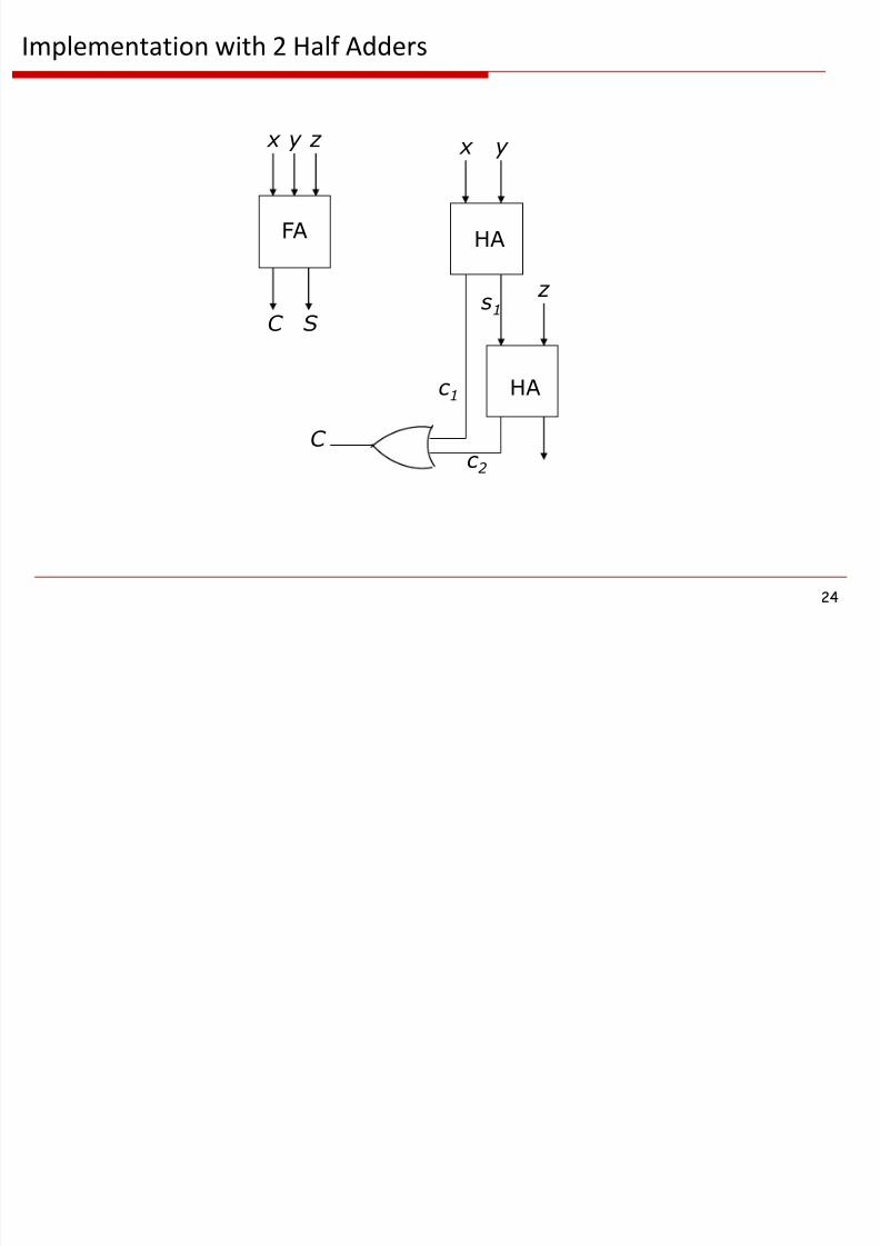
Implementation with 2 Half Adders
x y z
SC
FA
c 2
y x
HA
z
C
HA
s1
c 1
8/2/2019 rial Circuits
http://slidepdf.com/reader/full/rial-circuits 25/57
25
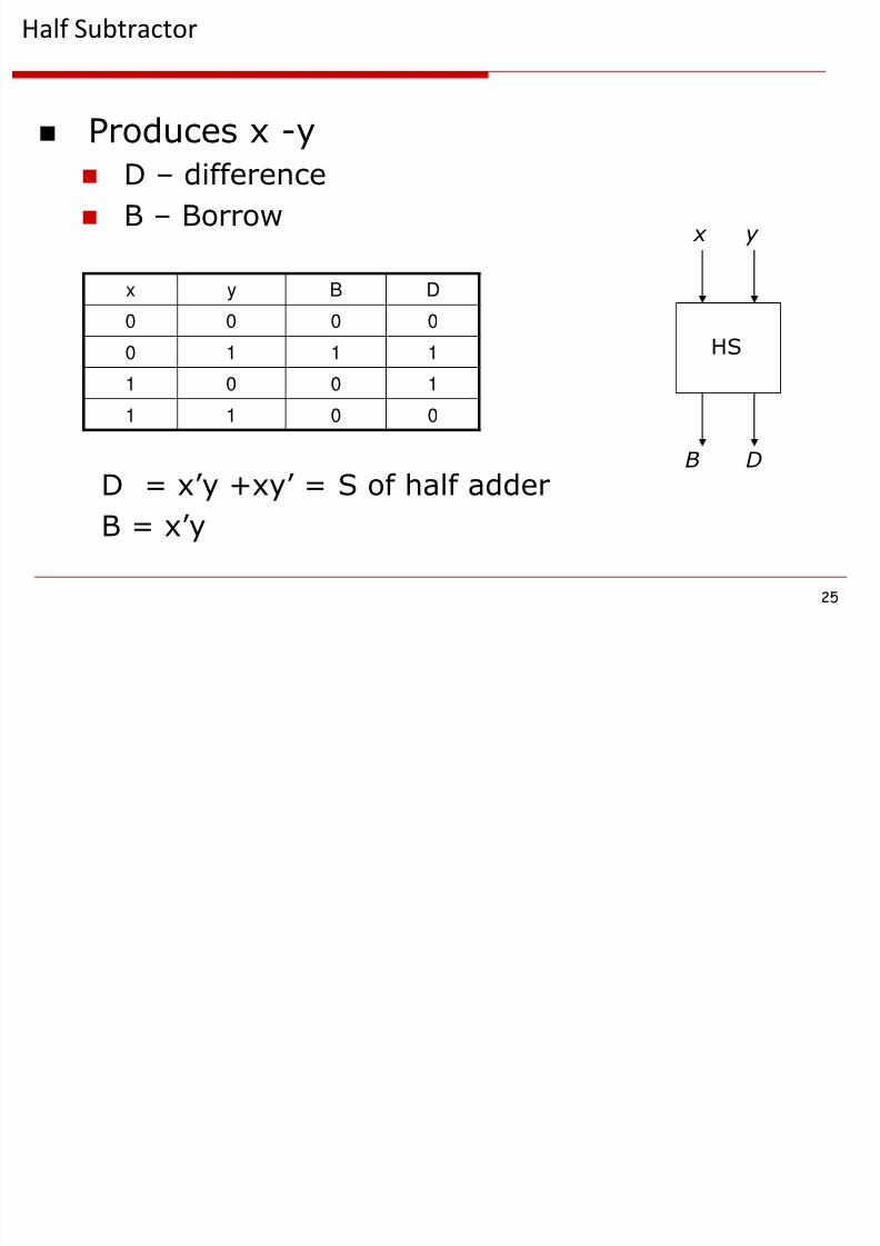
Half Subtractor
Produces x -y
D – difference
B – Borrow
x y B D
0 0 0 0
0 1 1 1
1 0 0 1
1 1 0 0
x y
B D
HS
D = x’y +xy’ = S of half adder
B = x’y
8/2/2019 rial Circuits
http://slidepdf.com/reader/full/rial-circuits 26/57
26
Full Subtractor
x y z B D
0 0 0 0 0
0 0 1 1 1
0 1 0 1 1
0 1 1 1 0
1 0 0 0 1
1 0 1 0 0
1 1 0 0 0
1 1 1 1 1
(x -y) –z; where z represents a borrow
D = x’y’z +x’yz’ + xy’z’ + xyz = xyz = S of full adder
B = x’y +x’z +yz (same as C of full adderexcept x is inverted
ll l dd
8/2/2019 rial Circuits
http://slidepdf.com/reader/full/rial-circuits 27/57
27
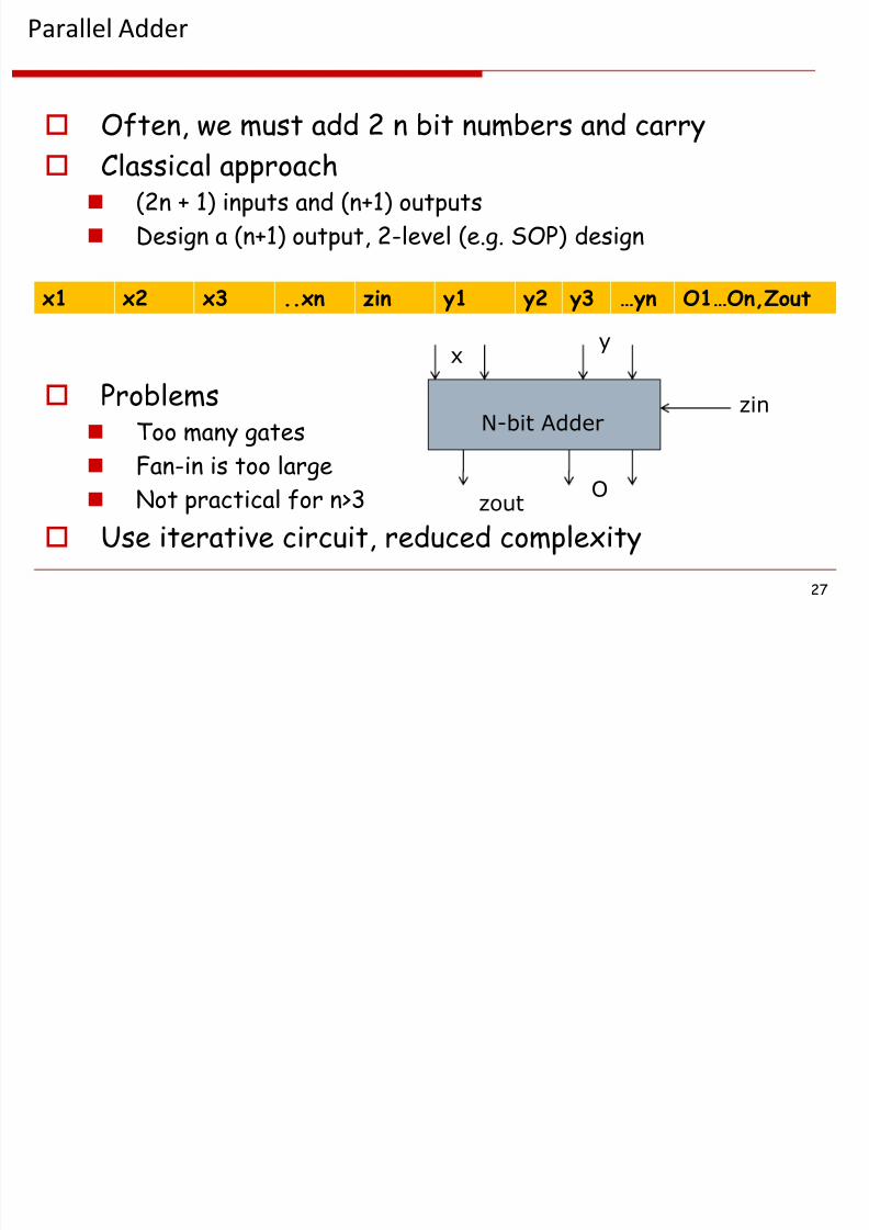
Parallel Adder
Often, we must add 2 n bit numbers and carry
Classical approach (2n + 1) inputs and (n+1) outputs
Design a (n+1) output, 2-level (e.g. SOP) design
Problems Too many gates
Fan-in is too large
Not practical for n>3
Use iterative circuit, reduced complexity
x1 x2 x3 ..xn zin y1 y2 y3 …yn O1…On,Zout
N-bit Adder
xy
zin
Ozout
8/2/2019 rial Circuits
http://slidepdf.com/reader/full/rial-circuits 28/57
28
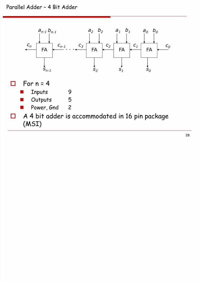
Parallel Adder – 4 Bit Adder
For n = 4 Inputs 9
Outputs 5
Power, Gnd 2
A 4 bit adder is accommodated in 16 pin package(MSI)
b0a0b1b2bn-1 a1a2an-1
s0s1s2sn-1
c 1c 2c 3c n-1c n. . .FA FA FA FA
c 0
Parallel Adder Issues
8/2/2019 rial Circuits
http://slidepdf.com/reader/full/rial-circuits 29/57
29
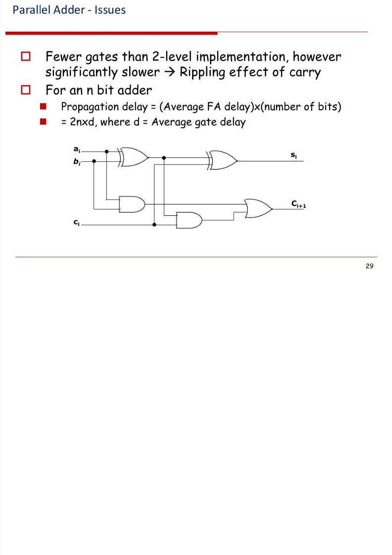
Parallel Adder - Issues
Fewer gates than 2-level implementation, however
significantly slower Rippling effect of carry For an n bit adder
Propagation delay = (Average FA delay)x(number of bits)
= 2nxd, where d = Average gate delay
ai
ci
sibi
Ci+1
C Ri l
8/2/2019 rial Circuits
http://slidepdf.com/reader/full/rial-circuits 30/57
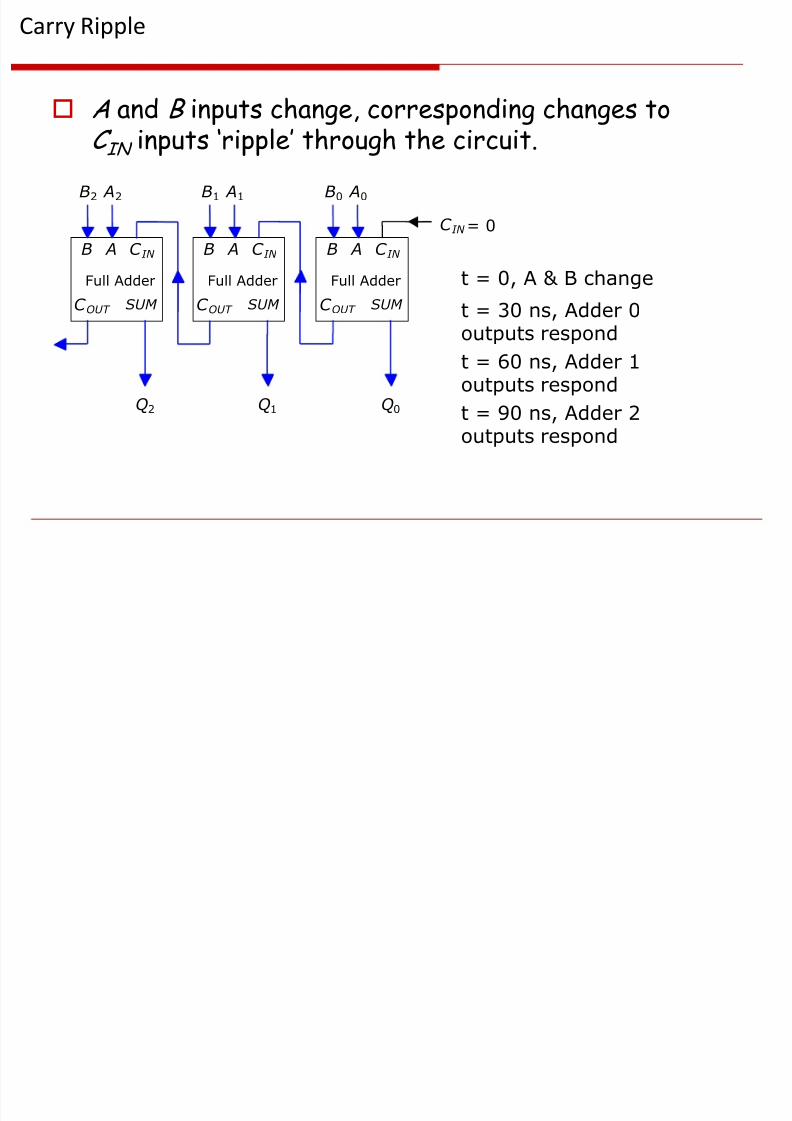
Carry Ripple
A and B inputs change, corresponding changes to
C IN inputs ‘ripple’ through the circuit.
Full Adder
B A C IN
C OUT SUM
Full Adder
B A C IN
C OUT SUM
Full Adder
B A C IN
C OUT SUM
B1 A1 B0 A0B2 A2
C IN = 0
Q1 Q0Q2
t = 0, A & B change
t = 30 ns, Adder 0outputs respond
t = 60 ns, Adder 1outputs respond
t = 90 ns, Adder 2outputs respond
C L k Ah d

8/2/2019 rial Circuits
http://slidepdf.com/reader/full/rial-circuits 31/57
Carry-Look-Ahead
The accumulated delay in large parallel adders can be prohibitively large.
Example : 16 bits using 30 ns full-adders :
Solution : Generate the carry-input signals directly from the A and B inputs ratherthan using the ripple arrangement.
ns480ns3016
D i i C L k Ah d Ci it
8/2/2019 rial Circuits
http://slidepdf.com/reader/full/rial-circuits 32/57
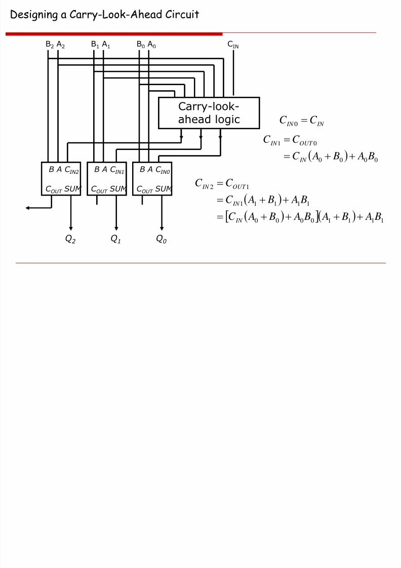
Designing a Carry-Look-Ahead Circuit
B A C IN2
C OUT SUM
B A C IN1
C OUT SUM
B A C IN0
C OUT SUM
Q2 Q1 Q0
Carry-look-ahead logic
B2 A2 B1 A1 B0 A0
11110000
11111
12
B A B A B A B AC
B A B AC
C C
IN
IN
OUT IN
CIN
0000
01
B A B AC
C C
IN
OUT IN
IN IN C C
0
C L k h d Add
8/2/2019 rial Circuits
http://slidepdf.com/reader/full/rial-circuits 33/57
E&CE 223 Digital Circuits and Systems (A. Kennings) Page 33
Carry Lookahead Adders
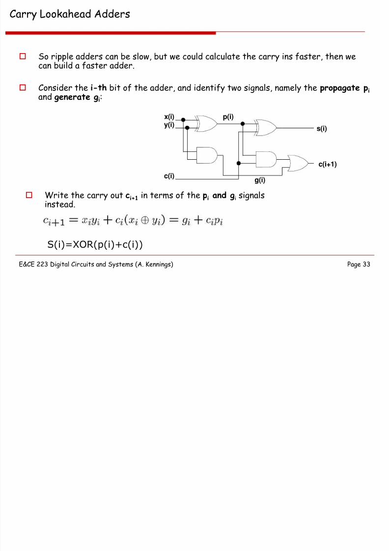
s(i)
c(i+1)
x(i)y(i)
c(i)g(i)
p(i)
So ripple adders can be slow, but we could calculate the carry ins faster, then we
can build a faster adder.
Consider the i-th bit of the adder, and identify two signals, namely the propagate piand generate gi:
Write the carry out ci+1 in terms of the pi and gi signalsinstead.
S(i)=XOR(p(i)+c(i))
W iti Th C i I T f P t d G t
8/2/2019 rial Circuits
http://slidepdf.com/reader/full/rial-circuits 34/57
E&CE 223 Digital Circuits and Systems (A. Kennings) Page 34
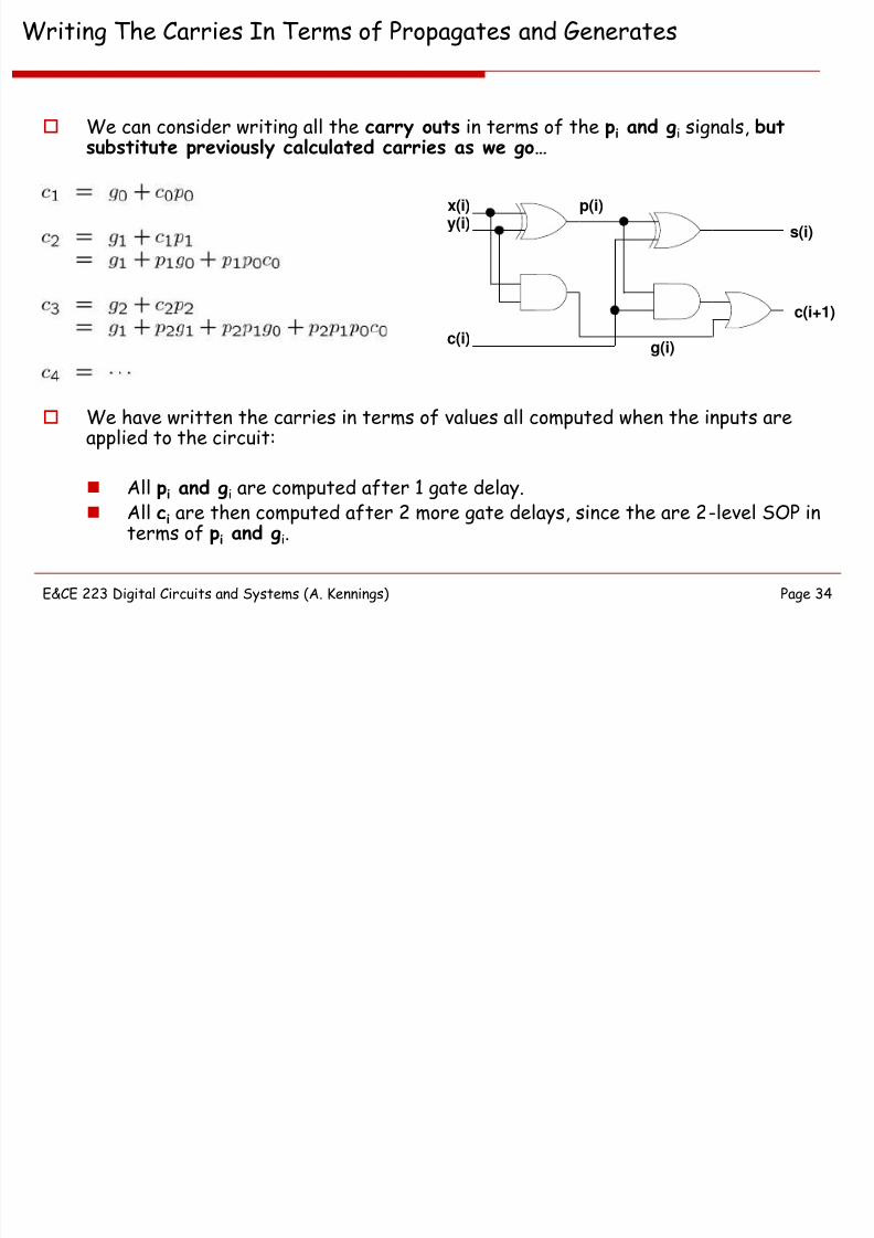
Writing The Carries In Terms of Propagates and Generates
We can consider writing all the carry outs in terms of the pi and gi signals, but
substitute previously calculated carries as we go…
We have written the carries in terms of values all computed when the inputs areapplied to the circuit:
All pi and gi are computed after 1 gate delay. All ci are then computed after 2 more gate delays, since the are 2-level SOP in
terms of pi and gi.
s(i)
c(i+1)
x(i)y(i)
c(i)g(i)
p(i)
C L k h d P f
8/2/2019 rial Circuits
http://slidepdf.com/reader/full/rial-circuits 35/57
E&CE 223 Digital Circuits and Systems (A. Kennings) Page 35
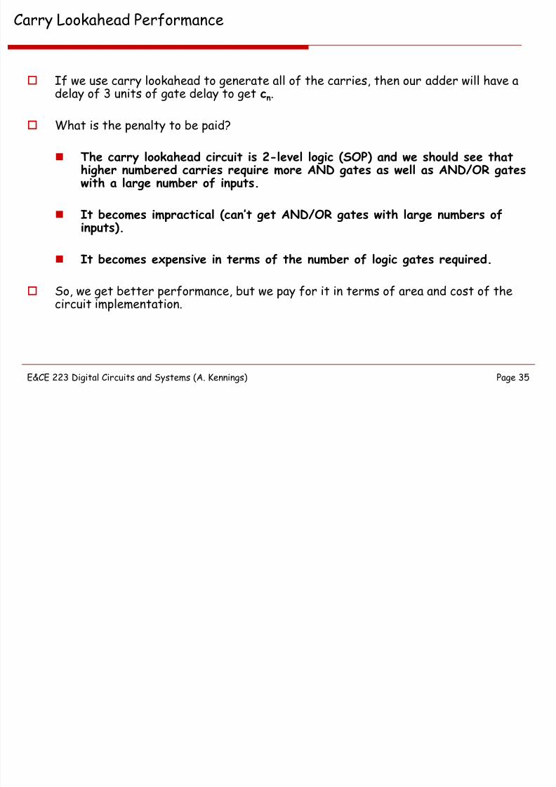
Carry Lookahead Performance
If we use carry lookahead to generate all of the carries, then our adder will have a
delay of 3 units of gate delay to get cn.
What is the penalty to be paid?
The carry lookahead circuit is 2-level logic (SOP) and we should see thathigher numbered carries require more AND gates as well as AND/OR gateswith a large number of inputs.
It becomes impractical (can’t get AND/OR gates with large numbers ofinputs).
It becomes expensive in terms of the number of logic gates required.
So, we get better performance, but we pay for it in terms of area and cost of thecircuit implementation.
C mbi i Ri l Add s d C L k h d
8/2/2019 rial Circuits
http://slidepdf.com/reader/full/rial-circuits 36/57
E&CE 223 Digital Circuits and Systems (A. Kennings) Page 36
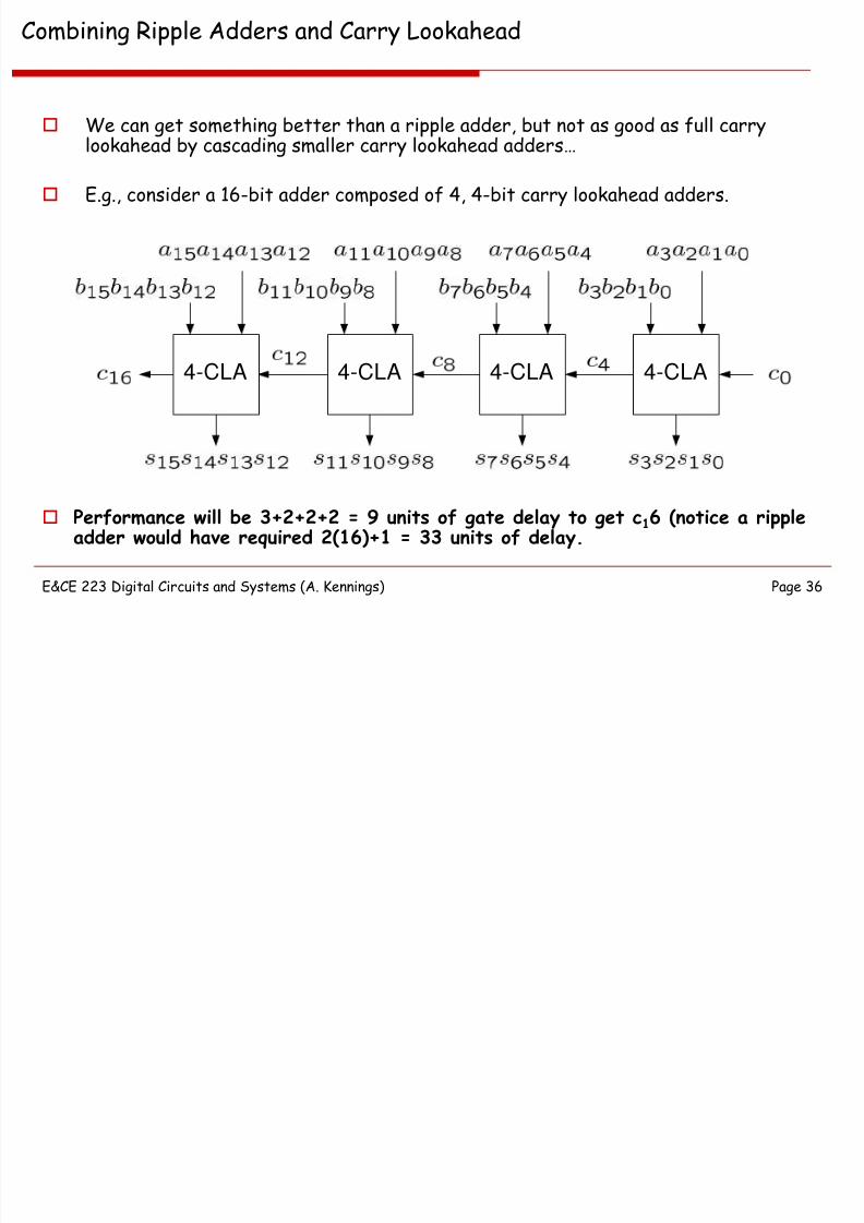
Combining Ripple Adders and Carry Lookahead
We can get something better than a ripple adder, but not as good as full carry
lookahead by cascading smaller carry lookahead adders…
E.g., consider a 16-bit adder composed of 4, 4-bit carry lookahead adders.
4-CLA 4-CLA4-CLA4-CLA
Performance will be 3+2+2+2 = 9 units of gate delay to get c16 (notice a rippleadder would have required 2(16)+1 = 33 units of delay.
Carry Lookahead Logic

8/2/2019 rial Circuits
http://slidepdf.com/reader/full/rial-circuits 37/57
37
Carry Lookahead Logic
4 Bit Add S bt t
8/2/2019 rial Circuits
http://slidepdf.com/reader/full/rial-circuits 38/57
38
4 Bit Adder Subtractor
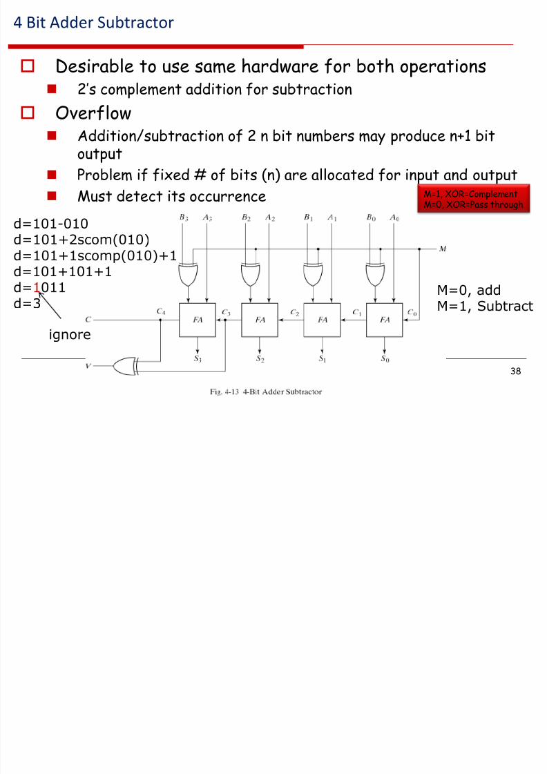
Desirable to use same hardware for both operations
2’s complement addition for subtraction Overflow
Addition/subtraction of 2 n bit numbers may produce n+1 bitoutput
Problem if fixed # of bits (n) are allocated for input and output
Must detect its occurrence
d=101-010d=101+2scom(010)d=101+1scomp(010)+1d=101+101+1
d=1011d=3
M=0, addM=1, Subtract
M=1, XOR=ComplementM=0, XOR=Pass through
ignore
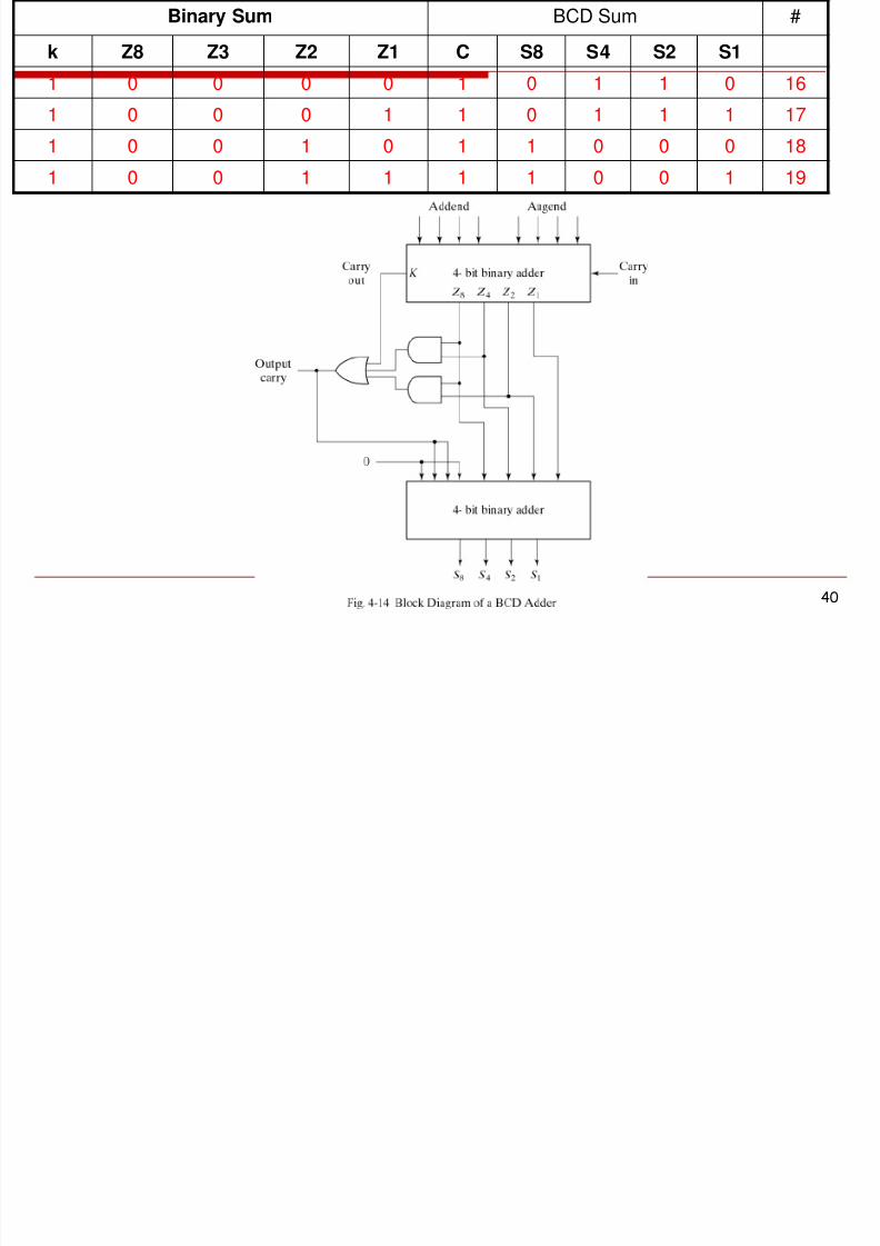
BCD Adder

8/2/2019 rial Circuits
http://slidepdf.com/reader/full/rial-circuits 39/57
39
BCD AdderBinary Sum BCD Sum #
k Z8 Z3 Z2 Z1 C S8 S4 S2 S1
0 0 0 0 0 0 0 0 0 0 0
0 0 0 0 1 0 0 0 0 1 1
0 0 0 1 0 0 0 0 1 0 2
0 0 0 1 1 0 0 0 1 1 3
0 0 1 0 0 0 0 1 0 0 4
0 0 1 0 1 0 0 1 0 1 50 0 1 1 0 0 0 1 1 0 6
0 0 1 1 1 0 0 1 1 1 7
0 1 0 0 0 0 1 0 0 0 8
0 1 0 0 1 0 1 0 0 1 9
0 1 0 1 0 1 0 0 0 0 10
0 1 0 1 1 1 0 0 0 1 11
0 1 1 0 0 1 0 0 1 0 12
0 1 1 0 1 1 0 0 1 1 13
0 1 1 1 0 1 0 1 0 0 14
0 1 1 1 1 1 0 1 0 1 15
Binary Sum BCD Sum #
8/2/2019 rial Circuits
http://slidepdf.com/reader/full/rial-circuits 40/57
40
k Z8 Z3 Z2 Z1 C S8 S4 S2 S1
1 0 0 0 0 1 0 1 1 0 16
1 0 0 0 1 1 0 1 1 1 17
1 0 0 1 0 1 1 0 0 0 18
1 0 0 1 1 1 1 0 0 1 19
Magnitude Comparator

8/2/2019 rial Circuits
http://slidepdf.com/reader/full/rial-circuits 41/57
41
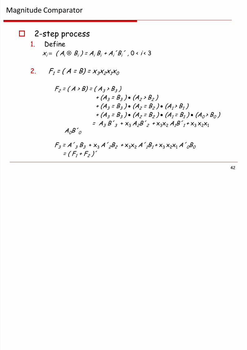
Magnitude Comparator
Classical approach
3 outputs and 2n inputs Large logic complexity, if n >3
Alternative Approach
2-step process
F 1
(A = B)
F 2 (A > B)
F 3 (A < B)
magnitudecomparator
4
4A
B
Magnit de Comparator
8/2/2019 rial Circuits
http://slidepdf.com/reader/full/rial-circuits 42/57
42
Magnitude Comparator
2-step process
1. Definex i ( A i B i ) = A i B i + A i ́ B i ́ , 0 < i < 3
2. F 1 = ( A = B) = x 3 x 2 x 1 x 0
F 2 = ( A > B) = ( A 3 > B 3 )
+ (A 3 = B 3 ) (A 2 > B 2 )
+ (A 3 = B 3 ) (A 2 = B 2 ) (A 1 > B 1 )
+ (A 3 = B 3 ) (A 2 = B 2 ) (A 1 = B 1 ) (A 0 > B 0 )
= A 3 B´ 3 + x3 A 2 B´ 2 + x3x2 A 1 B´ 1 + x3 x2x1
A 0 B´ 0
F 3 = A´ 3 B 3 + x3 A´ 2 B 2 + x3x2 A´ 1 B 1 + x3 x2x1 A´ 0 B 0
= ( F 1 + F 2 )´
Magnitude Comparator
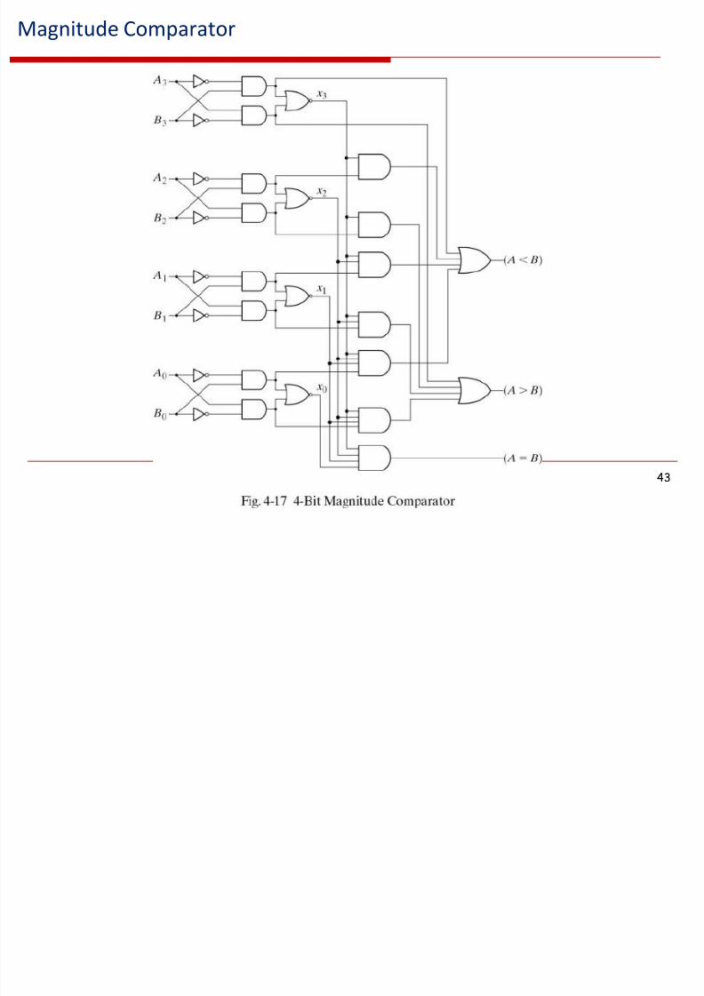
8/2/2019 rial Circuits
http://slidepdf.com/reader/full/rial-circuits 43/57
43
Magnitude Comparator
Decoders
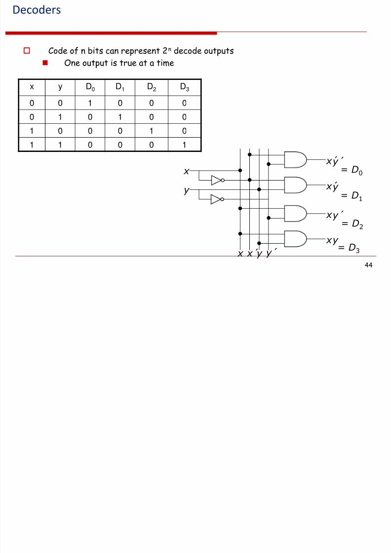
8/2/2019 rial Circuits
http://slidepdf.com/reader/full/rial-circuits 44/57
44
Code of n bits can represent 2n decode outputs
One output is true at a time
x
y
x y x´
x
y x´
y´
y´
y´
x´
xy
x y D0 D1 D2 D3
0 0 1 0 0 0
0 1 0 1 0 0
1 0 0 0 1 0
1 1 0 0 0 1
= D0
= D1
= D2
= D3
D d ith E bl
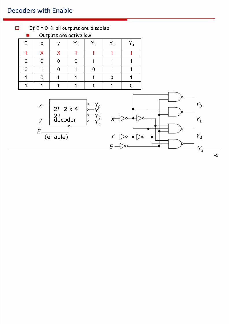
8/2/2019 rial Circuits
http://slidepdf.com/reader/full/rial-circuits 45/57
45
Decoders with Enable
If E = 0 all outputs are disabled
Outputs are active low
E x y Y0 Y1 Y2 Y3
1 X X 1 1 1 1
0 0 0 0 1 1 1
0 1 0 1 0 1 1
1 0 1 1 1 0 1
1 1 1 1 1 1 0
Y 0
Y 1
Y 2
Y 3E
x
y
Y 0Y 1
E
y
x
Y 2Y 3
21 2 x 4
20
decoder
(enable)
Larger Decoders
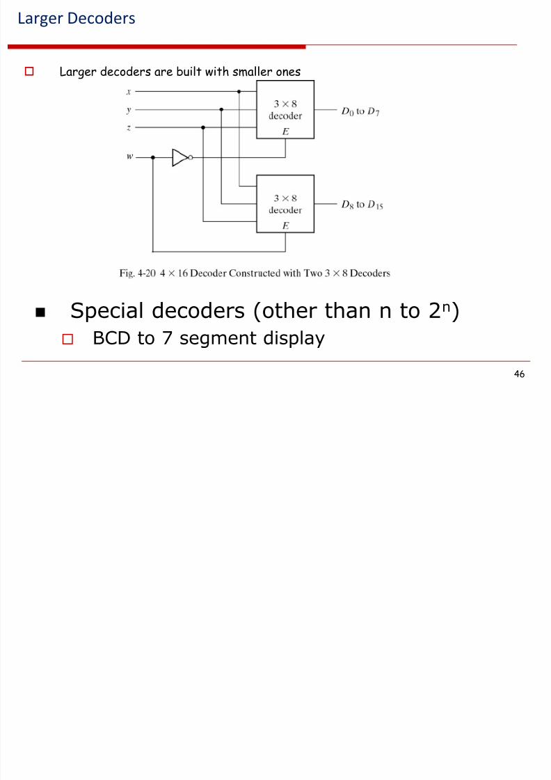
8/2/2019 rial Circuits
http://slidepdf.com/reader/full/rial-circuits 46/57
46
Larger Decoders
Larger decoders are built with smaller ones
Special decoders (other than n to 2n)
BCD to 7 segment display
F ti i l t ti i D d
8/2/2019 rial Circuits
http://slidepdf.com/reader/full/rial-circuits 47/57
47
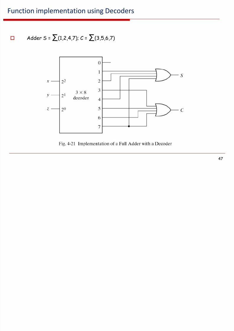
Function implementation using Decoders
Adder S = ∑(1,2,4,7); C = ∑(3,5,6,7)
Decoder based realization
8/2/2019 rial Circuits
http://slidepdf.com/reader/full/rial-circuits 48/57
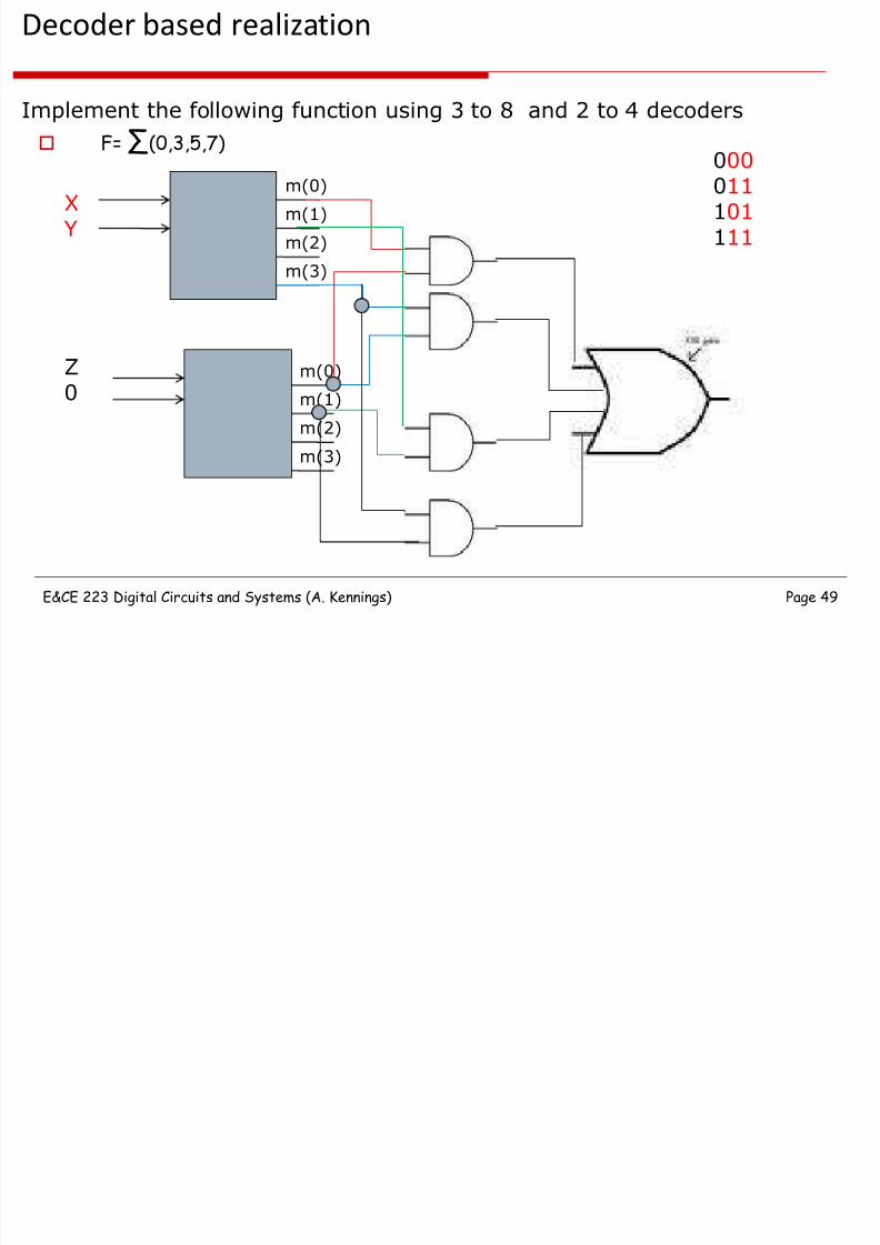
E&CE 223 Digital Circuits and Systems (A. Kennings) Page 48
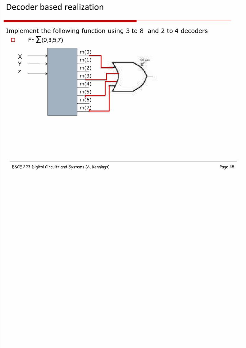
Implement the following function using 3 to 8 and 2 to 4 decoders
F= ∑(0,3,5,7)
XYz
m(0)
m(1)
m(4)
m(3)
m(6)
m(5)
m(2)
m(7)
Decoder based realization
8/2/2019 rial Circuits
http://slidepdf.com/reader/full/rial-circuits 49/57
E&CE 223 Digital Circuits and Systems (A. Kennings) Page 49
Implement the following function using 3 to 8 and 2 to 4 decoders
F= ∑(0,3,5,7)
XY
m(0)
m(1)
m(3)
m(2)
000011101111
Z0
m(0)
m(1)
m(3)
m(2)
Encoders

8/2/2019 rial Circuits
http://slidepdf.com/reader/full/rial-circuits 50/57
50
Does reverse operation to decoder
Constraint – only one input is active at a time
Example, Octal to Binary EncoderZ = D1 +D3 +D5 +D7; y = D2 +D3 +D6 +D7; x = D4 +D5 +D6 +D7
Inputs Outputs
D0 D1 D2 D3 D4 D5 D6 D7 x y z1 0 0 0 0 0 0 0 0 0 0
0 1 0 0 0 0 0 0 0 0 1
0 0 1 0 0 0 0 0 0 1 0
0 0 0 1 0 0 0 0 0 1 1
0 0 0 0 1 0 0 0 1 0 0
0 0 0 0 0 1 0 0 1 0 1
0 0 0 0 0 0 1 0 1 1 0
0 0 0 0 0 0 0 1 1 1 1
Priority Encoders

8/2/2019 rial Circuits
http://slidepdf.com/reader/full/rial-circuits 51/57
51
Priority Encoders
Encoder with priority function Multiple inputs may be true simultaneously
Higher priority input gets the precedence
Inputs Outputs
D0 D1 D2 D3 x y V
0 0 0 0 X X 0
1 0 0 0 0 0 1
X 1 0 0 0 1 1
X X 1 0 1 0 1
X X X 1 1 1 1
Valid bit, V, indicates one or more inputs are trueat the same time
Higher priority input gets the precedence
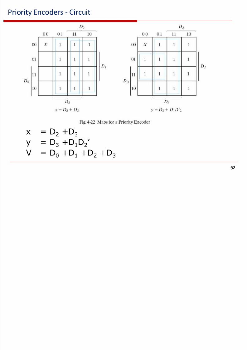
Priority Encoders Circuit
8/2/2019 rial Circuits
http://slidepdf.com/reader/full/rial-circuits 52/57
52
Priority Encoders - Circuit
x = D2 +D3
y = D3 +D1D2’
V = D0 +D1 +D2 +D3
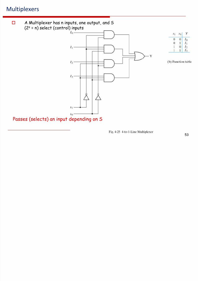
Multiplexers
8/2/2019 rial Circuits
http://slidepdf.com/reader/full/rial-circuits 53/57
53
Multiplexers
A Multiplexer has n inputs, one output, and S(2s = n) select (control) inputs
Passes (selects) an input depending on S
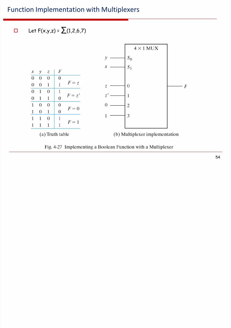
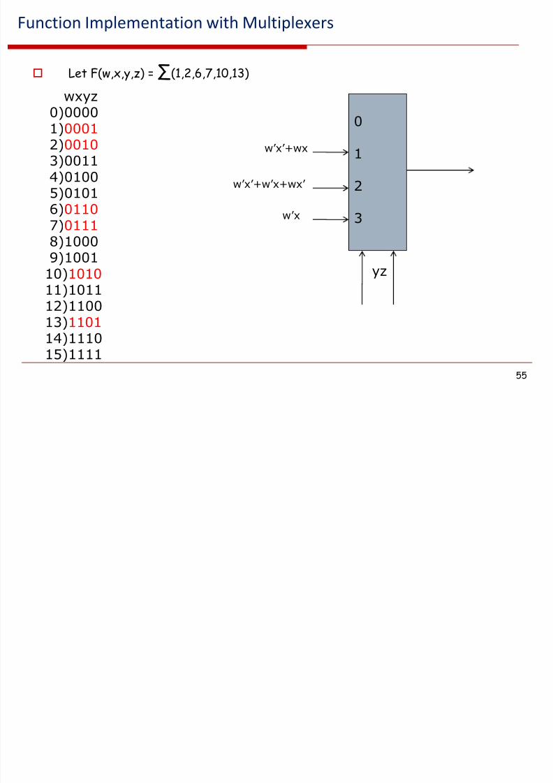
Function Implementation with Multiplexers
8/2/2019 rial Circuits
http://slidepdf.com/reader/full/rial-circuits 54/57
54
Function Implementation with Multiplexers
Let F(x,y,z) = ∑(1,2,6,7)
Function Implementation with Multiplexers
8/2/2019 rial Circuits
http://slidepdf.com/reader/full/rial-circuits 55/57
55
Function Implementation with Multiplexers
Let F(w,x,y,z) = ∑(1,2,6,7,10,13)
wxyz0)00001)00012)00103)00114)0100
5)01016)01107)01118)10009)100110)1010
11)101112)110013)110114)111015)1111
0
1
2
3
yz
w’x’+wx
w’x’+w’x+wx’
w’x
Multiplexers with Tri-stated Gates
8/2/2019 rial Circuits
http://slidepdf.com/reader/full/rial-circuits 56/57
56
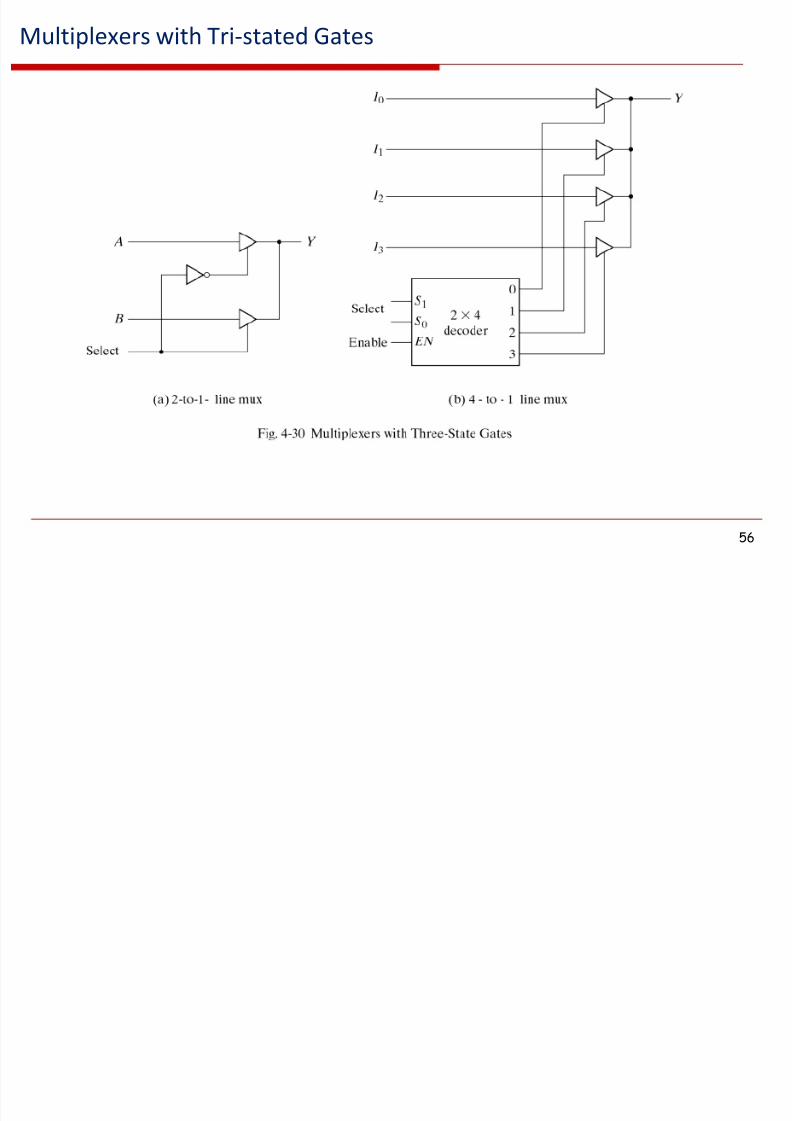
Multiplexers with Tri-stated Gates

8/2/2019 rial Circuits
http://slidepdf.com/reader/full/rial-circuits 57/57
57
Book Sections – Combination Circuits
Material is covered in Sections 4.1 – 4.5, 4.7 – 4.10