Review - Santa Cruz Institute for Particle...
30
Review Energy Bands Carrier Density & Mobility Carrier Transport Generation and Recombination
Transcript of Review - Santa Cruz Institute for Particle...

Review
Energy Bands Carrier Density & Mobility
Carrier Transport Generation and Recombination

The Metal-Semiconductor Junction: Review
Energy band diagram of the metal and the semiconductor before (a) and after (b) contact
Barrier Height
Built-in Potential

M-S Junctions: Thermal Equilibrium
Energy band diagram of a metal-semiconductor contact in thermal equilibrium.
De
ple
tio
n R
eg
ion
Under Bias

Full depletion approximation Review
(a) Charge density, (b) electric field, (c) potential and (d) energy with the full depletion analysis.

MOS Capacitors: Review
The MOS capacitor consists of a Metal-Oxide-Semiconductor structure
Current Transport at the MS Interface
The current across a metal-semiconductor junction is mainly due to majority carriers. Three
distinctly different mechanisms exist: diffusion of carriers from the semiconductor into the
metal, thermionic emission of carriers across the Schottky barrier and quantum-mechanical
tunneling through the barrier.
Diffusion Current: driving force is distributed over the length of the depletion layer.
Thermionic Emission: only energetic carriers, with energy equal to or larger than the
conduction band energy at the metal-semiconductor interface, contribute to the current flow.
Tunneling: the wave-nature of the electrons, allowing them to penetrate through thin
barriers.
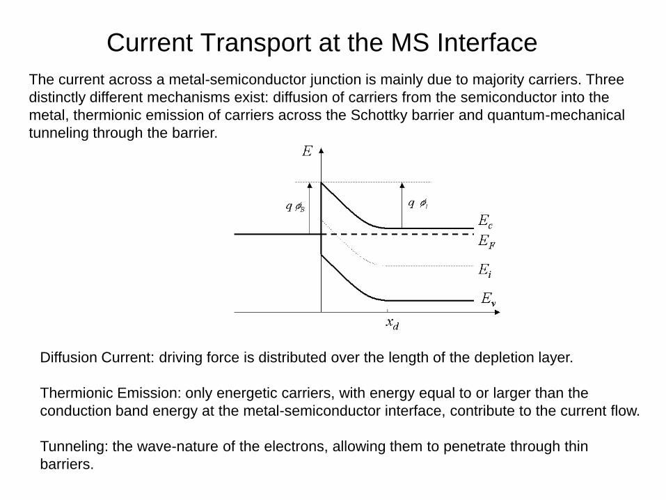
Diffusion, Thermionic Emission & Tunneling
The thermionic emission theory assumes that electrons, with an energy larger than the top
of the barrier, will cross the barrier provided they move towards the barrier. The actual
shape of the barrier is ignored.
Richardson’s Constant
B is the Schottky barrier height.
and velocity
For tunneling, the carrier density equals the density of available electrons, n, multiplied
with the tunneling probability, , yielding:
where = B/L
For Diffusion current, the depletion layer is large compared to the mean free path, so that
the concepts of drift and diffusion are valid. The current depends exponentially on the
applied voltage, Va, and the barrier height, B.
Electric-field at
MS Junction:

Metal-Semiconductor Contacts
MS contacts cannot be assumed to have a
resistance as low as that of two connected
metals. In particular, a large mismatch
between the Fermi energy of the metal and
semiconductor can result is a high-resistance
rectifying contact. Low resistance Ohmic
contacts or tunnel contacts can be created.
Tunnel contacts have a positive barrier at the MS interface, but also have a high enough
doping in the semiconductor that there is only a thin barrier separating the metal from the
semiconductor. If the width of the depletion region at the MS interface is very thin, on the
order of 3 nm or less, carriers can readily tunnel across such barrier. The typical required
doping density for such contact is 1019 cm-3 or higher.
Ohmic contacts exist if the Schottky barrier height, B, is zero or negative. For an n-type
semiconductor, M is close or smaller than . For a p-type semiconductor, M is close or
greater than + Eg

Different methods of forming Contacts
Ohmic:
A high temperature step is used so metal can either alloy with the semiconductor or
reduce the unintentional barrier at the interface.
n and p-doping are frequently used as a method to form Ohmic contacts.
Tunneling Contacts:
Contacts deposited at Low-T tend to form Shottky barriers, or tunneling, contacts
Pinning of the Fermi energy at the interface due to the large number of surface states
at the metal-semiconductor interface can also occur, leading to a tunneling contact.

Contact Resistance
This equivalent circuit is obtained by slicing the structure into small sections with length
x.
The contact resistance, R1, and the semiconductor resistance, R2, are given by:
where c is the contact resistance of the metal-to-semiconductor interface per unit area with
units of cm2, Rs is the sheet resistance of the semiconductor layer with units of Ohms per
square, and W is the width of the contact.

Contact Resistance
Kirchoff’s Laws:
Letting x go to 0:
is the characteristic distance over which the
current changes under the metal contact and is
also referred to as the penetration length.
Lateral current and voltage underneath a 5 mm long and 1 mm
wide metal contact with a c of 10-5 -cm2 on a thin
semiconductor layer with a Rs of 100 Ohms per sq.

Currents Through Insulators
Current mechanisms through materials which do not contain free carriers (i.e. insulators) can
be distinctly different from those in doped semiconductors or metals.
Fowler-Nordheim Tunneling: carriers quantum mechanically tunnel from the conductor into the
insulator.
Poole-Frenkel emission: Traps restrict current flow because of a capture and emission process
Space charge Limited Current: A high density of charged carriers causes a field gradient, which
limits the current density.
Ballistic transport: Carrier transport without scattering or any other mechanism, which would
cause a loss of energy.

Fowler-Nordheim Tunneling
Fowler-Nordheim tunneling has been studied extensively in Metal-Oxide-Semiconductor
structures where it is the dominant current mechanism, especially for thick oxides.
Quantum mechanical tunneling from the adjacent conductor into the insulator limits the
current through the structure. Once the carriers have tunneled into the insulator they
are free to move within the valence or conduction band of the insulator. The calculation
of the current is based on the WKB approximation yielding the following relation
between the current density, JFN, and the electric field in the oxide, ox:
For tunneling
To check for this current mechanism, experimental I-V characteristics are typically
plotted as ln(JFN / ox) versus 1/ ox, a so-called Fowler-Nordheim plot. Provided the
effective mass of the insulator is known, one can then fit the experimental data to a
straight line yielding a value for the barrier height.

Poole-Frenkel Emission
Structural defects can cause additional energy states close to the band edge, called traps.
These traps restrict the current flow because of a capture and emission process, thereby
becoming the dominant current mechanism. The current is a simple drift current described by:
while the carrier density depends exponentially on the depth of the trap, which is
corrected for the electric field
The total current then equals:

Space Charge Limited Current
Both Fowler-Nordheim tunneling and Poole-Frenkel emission mechanism yield very low
current densities with correspondingly low carrier densities. For structures where
carriers can readily enter the insulator and freely flow through the insulator one finds
that the resulting current and carrier densities are much higher. The high density of
these charged carriers causes a field gradient, which limits the current density.
Some math (see HW problem):

Ballistic Transport
Ballistic transport is carrier transport without scattering or any other mechanism, which
would cause a loss of energy. Combining energy conservation, current continuity and
Gauss's law one finds the following current-voltage relation:
where d is the thickness of the insulator and m* is the effective mass of the carriers.

The p-n Junction
A p-n junction consists of two semiconductor regions with opposite doping type. The region
on the left is p-type with an acceptor density Na, and on the right is n-type with a donor
density Nd. The dopants are assumed to be shallow, so that the electron (hole) density in
the n-type (p-type) region is approximately equal to the donor (acceptor) density.
Abrupt p-n junction: the doped regions are uniformly doped sp that the transition
between the two regions is abrupt.
One-sided abrupt p-n junction: one side of the p-n junctions in is distinctly higher-
doped than the other in which case only the low-doped region needs to be considered.

The p-n Junction under bias
The junction is biased with a voltage Va.
Forward-biased: a positive voltage is applied to the p-doped region
Reversed-biased: a negative voltage is applied to the p-doped region.
Anode: the p-type region
Cathode: the n-type region

The p-n Junction: Flat Band Diagram
Energy band diagram of a p-n junction (a) before and (b) after merging the n-type and p-type regions
The flatband diagram is not an equilibrium diagram since both electrons and
holes can lower their energy by crossing the junction. The flatband diagram
implies that there is no field and no net charge in the semiconductor.

The p-n Junction: Thermal Equilibrium
• To reach thermal equilibrium,
electrons/holes diffuse across the junction
into the p-type/n-type region.
• This process leaves the ionized donors
(acceptors) behind, creating a region around
the junction, which is depleted of mobile
carriers. The depletion region extends from
x = -xp to x = xn.
• The charge due to the ionized donors and
acceptors causes an electric field, which in
turn causes a drift of carriers in the opposite
direction.
• The diffusion of carriers continues until the
drift current balances the diffusion current,
thereby reaching thermal equilibrium as
indicated by a constant Fermi energy.

The p-n Junction: Built-in Potential
While in thermal equilibrium no external voltage is
applied between the n-type and p-type material, there
is an internal potential, i, or built-in potential, which is
caused by the workfunction difference between the n-
type and p-type semiconductors.
The built-in potential in a semiconductor equals the
potential across the depletion region in thermal
equilibrium. Since thermal equilibrium implies that the
Fermi energy is constant throughout the p-n diode,
the built-in potential equals the difference between
the Fermi energies, EFn and EFp, divided by the
electronic charge.
It also equals the sum of the bulk potentials of each
region, n and p, since the bulk potential quantifies
the distance between the Fermi energy and the
intrinsic energy.
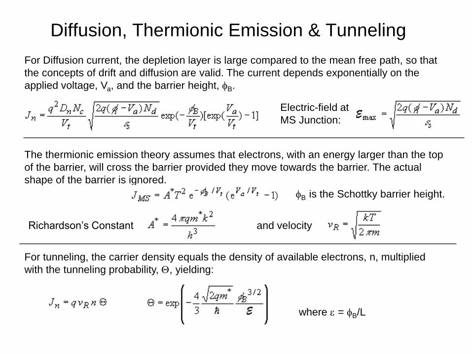
The p-n Junction: Built-in Potential
An abrupt silicon p-n junction consists of a p-type region containing 2 x 1016 cm-3 acceptors and an
n-type region containing also 1016 cm-3 acceptors in addition to 1017 cm-3 donors.
1. Calculate the thermal equilibrium density of electrons and holes in the p-type region as well as
both densities in the n-type region.
2. Calculate the built-in potential of the p-n junction
Solution
1. The thermal equilibrium densities are:
In the p-type region:
p = Na = 2 x 1016 cm-3
n = ni2/p = 1020/2 x 1016 = 5 x 103 cm-3
In the n-type region
n = Nd - Na = 9 x 1016 cm-3
p = ni2/n = 1020/(1 x 1016) = 1.11 x 103 cm-3
2. The built-in potential is obtained from:

The p-n Junction: Forward and Reverse Bias
As a negative voltage is applied, the potential across the semiconductor increases
and so does the depletion layer width. As a positive voltage is applied, the potential
across the semiconductor decreases and with it the depletion layer width. The total
potential across the semiconductor equals the built-in potential minus the applied
voltage, or:
Energy band diagram of a p-n junction under reverse and forward bias

The p-n Junction vs MS Junction

The p-n Junction: Poisson’s Equation
The electrostatic analysis of a p-n diode is of interest since it provides knowledge
about the charge density and the electric field in the depletion region. A key
difference to MS junction is that a p-n diode contains two depletion regions of
opposite type.The general analysis starts by setting up Poisson's equation:
This second-order non-linear differential equation cannot be solved analytically.
A simplifying assumption that the depletion region is fully depleted and that the adjacent
neutral regions contain no charge is made, known as the full depletion approximation.
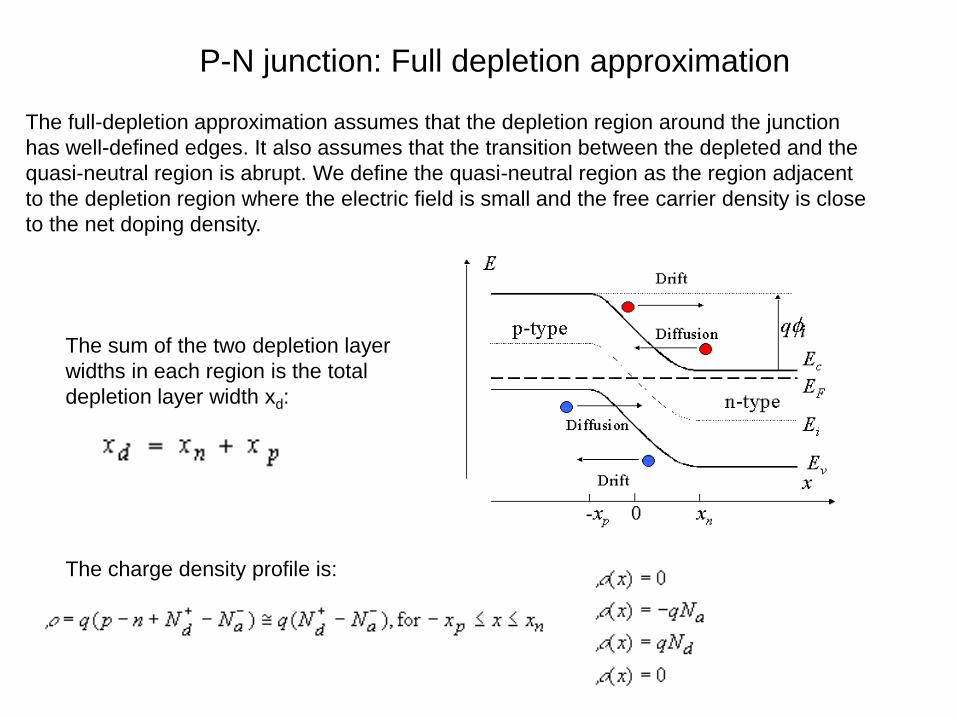
P-N junction: Full depletion approximation
The full-depletion approximation assumes that the depletion region around the junction
has well-defined edges. It also assumes that the transition between the depleted and the
quasi-neutral region is abrupt. We define the quasi-neutral region as the region adjacent
to the depletion region where the electric field is small and the free carrier density is close
to the net doping density.
The sum of the two depletion layer
widths in each region is the total
depletion layer width xd:
The charge density profile is:

P-N junction: Full depletion approximation
(a) Charge density in a p-n junction, (b) Electric field, (c) Potential and (d) Energy band diagram

P-N junction: Full depletion approximation
The charge in the n-type region, Qn, and the charge in the p-type region, Qp, are given by:
Gauss’s Law:
This maximum field can be calculated on either side of the depletion region, yielding:
Relationship between 2 unknowns:

P-N junction: Full depletion approximation
The potential in the semiconductor is obtained from the electric field using:
The total potential across the semiconductor must equal the difference between the built-in
potential and the applied voltage, which provides a second relation between xp and xn:

P-N junction: Full depletion approximation
An abrupt silicon (nI = 1010 cm-3) p-n junction consists of a p-type region containing 1016 cm-3 acceptors
and an n-type region containing 5 x 10¹⁶ c cm-3 donors.
1. Calculate the built-in potential of this p-n junction.
2. Calculate the total width of the depletion region if the applied voltage Va equals 0, 0.5 and -2.5 V.
3. Calculate maximum electric field in the depletion region at 0, 0.5 and -2.5 V.
4. Calculate the potential across the depletion region in the n-type semiconductor at 0, 0.5 and -2.5 V.
Solution
The built-in potential is calculated from:
The depletion layer width is obtained from:
the electric field from
and the potential across the n-type region equals where