Reliability Analysis and Performance Degradation of a ...
9
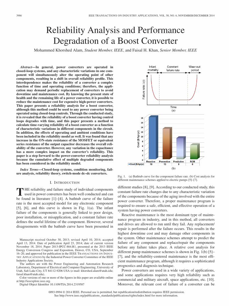
3986 IEEE TRANSACTIONS ON INDUSTRY APPLICATIONS, VOL. 50, NO. 6, NOVEMBER/DECEMBER 2014 Reliability Analysis and Performance Degradation of a Boost Converter Mohammed Khorshed Alam, Student Member, IEEE, and Faisal H. Khan, Senior Member, IEEE Abstract—In general, power converters are operated in closed-loop systems, and any characteristic variations in one com- ponent will simultaneously alter the operating point of other components, resulting in a shift in overall reliability profile. This interdependence makes the reliability of a converter a complex function of time and operating conditions; therefore, the appli- cation may demand periodic replacement of converters to avoid downtime and maintenance cost. By knowing the present state of health and the remaining life of a power converter, it is possible to reduce the maintenance cost for expensive high-power converters. This paper presents a reliability analysis for a boost converter, although this method could be used to any power converter being operated using closed-loop controls. Through the conducted study, it is revealed that the reliability of a boost converter having control loops degrades with time, and this paper presents a method to calculate time-varying reliability of a boost converter as a function of characteristic variations in different components in the circuit. In addition, the effects of operating and ambient conditions have been included in the reliability model as well. It was found that any increase in the ON-state resistance of the MOSFET or equivalent series resistance of the output capacitor decreases the overall reli- ability of the converter. However, any variation in the capacitance has a more complex impact on the converter’s reliability. This paper is a step forward to the power-converter reliability analysis because the cumulative effect of multiple degraded components has been considered in the reliability model. Index Terms—Closed-loop systems, condition monitoring, fail- ure analysis, reliability theory, switch-mode dc–dc converters. I. I NTRODUCTION T HE reliability and failure study of individual components used in power converters has been well conducted and can be found in literature [1]–[4]. A bathtub curve of the failure rate is the most accepted model for any electronic component [5], [6], and this curve is shown in Fig. 1(a). The infant failure of the components is generally linked to poor design, poor installation, or misapplication, and a constant failure rate defines the useful lifetime of the component. However, several disagreements with the bathtub curve have been presented in Manuscript received October 30, 2013; revised April 10, 2014; accepted April 13, 2014. Date of publication April 23, 2014; date of current version November 18, 2014. Paper 2013-IPCC-864.R1, presented at the 2013 IEEE Energy Conversion Congress and Exposition, Denver, CO, USA, September 16–20, and approved for publication in the IEEE TRANSACTIONS ON I NDUS- TRY APPLICATIONS by the Industrial Power Converter Committee of the IEEE Industry Applications Society. The authors are with the Power Engineering and Automation Research Laboratory, Department of Electrical and Computer Engineering, University of Utah, Salt Lake City, UT 84112-9206 USA (e-mail: [email protected]; [email protected]). Color versions of one or more of the figures in this paper are available online at http://ieeexplore.ieee.org. Digital Object Identifier 10.1109/TIA.2014.2319587 Fig. 1. (a) Bathtub curve for the component failure rate. (b) Cost analysis for different maintenance schemes applied to electric pumps [5]–[7]. different studies [8], [9]. According to our conducted study, this constant failure rate changes due to any characteristic variation of the components because of the aging involved with the entire power converter. Therefore, a proper maintenance program is required to ensure a safe, efficient, and effective operation of a system having power converters. Reactive maintenance is the most dominant type of mainte- nance program in industry, and in this method, all converters and drives are allowed to run until they fail. Any replacement/ repair is performed after the failure occurs. This results in the highest downtime cost and may damage other components in the system. Other maintenance schemes attempt to predict the failure of any component and replace/repair the components before any failure takes place. A relative cost analysis for different pump maintenance schemes is shown in Fig. 1(b) [5]– [7], and the reliability-centered maintenance is the most effi- cient maintenance program, although it requires a sophisticated prognostics and diagnosis technique. Power converters are used in a wide variety of applications, and some applications requires very high reliability such as commercial and military aircraft, space applications, etc. [10]. Moreover, the relevant cost of failure of a converter can be 0093-9994 © 2014 IEEE. Personal use is permitted, but republication/redistribution requires IEEE permission. See http://www.ieee.org/publications_standards/publications/rights/index.html for more information.
Transcript of Reliability Analysis and Performance Degradation of a ...
3986 IEEE TRANSACTIONS ON INDUSTRY APPLICATIONS, VOL. 50, NO. 6, NOVEMBER/DECEMBER 2014
Reliability Analysis and PerformanceDegradation of a Boost Converter
Mohammed Khorshed Alam, Student Member, IEEE, and Faisal H. Khan, Senior Member, IEEE
Abstract—In general, power converters are operated inclosed-loop systems, and any characteristic variations in one com-ponent will simultaneously alter the operating point of othercomponents, resulting in a shift in overall reliability profile. Thisinterdependence makes the reliability of a converter a complexfunction of time and operating conditions; therefore, the appli-cation may demand periodic replacement of converters to avoiddowntime and maintenance cost. By knowing the present state ofhealth and the remaining life of a power converter, it is possible toreduce the maintenance cost for expensive high-power converters.This paper presents a reliability analysis for a boost converter,although this method could be used to any power converter beingoperated using closed-loop controls. Through the conducted study,it is revealed that the reliability of a boost converter having controlloops degrades with time, and this paper presents a method tocalculate time-varying reliability of a boost converter as a functionof characteristic variations in different components in the circuit.In addition, the effects of operating and ambient conditions havebeen included in the reliability model as well. It was found that anyincrease in the ON-state resistance of the MOSFET or equivalentseries resistance of the output capacitor decreases the overall reli-ability of the converter. However, any variation in the capacitancehas a more complex impact on the converter’s reliability. Thispaper is a step forward to the power-converter reliability analysisbecause the cumulative effect of multiple degraded componentshas been considered in the reliability model.
Index Terms—Closed-loop systems, condition monitoring, fail-ure analysis, reliability theory, switch-mode dc–dc converters.
I. INTRODUCTION
THE reliability and failure study of individual componentsused in power converters has been well conducted and can
be found in literature [1]–[4]. A bathtub curve of the failurerate is the most accepted model for any electronic component[5], [6], and this curve is shown in Fig. 1(a). The infantfailure of the components is generally linked to poor design,poor installation, or misapplication, and a constant failure ratedefines the useful lifetime of the component. However, severaldisagreements with the bathtub curve have been presented in
Manuscript received October 30, 2013; revised April 10, 2014; acceptedApril 13, 2014. Date of publication April 23, 2014; date of current versionNovember 18, 2014. Paper 2013-IPCC-864.R1, presented at the 2013 IEEEEnergy Conversion Congress and Exposition, Denver, CO, USA, September16–20, and approved for publication in the IEEE TRANSACTIONS ON INDUS-TRY APPLICATIONS by the Industrial Power Converter Committee of the IEEEIndustry Applications Society.
The authors are with the Power Engineering and Automation ResearchLaboratory, Department of Electrical and Computer Engineering, University ofUtah, Salt Lake City, UT 84112-9206 USA (e-mail: [email protected];[email protected]).
Color versions of one or more of the figures in this paper are available onlineat http://ieeexplore.ieee.org.
Digital Object Identifier 10.1109/TIA.2014.2319587
Fig. 1. (a) Bathtub curve for the component failure rate. (b) Cost analysis fordifferent maintenance schemes applied to electric pumps [5]–[7].
different studies [8], [9]. According to our conducted study, thisconstant failure rate changes due to any characteristic variationof the components because of the aging involved with the entirepower converter. Therefore, a proper maintenance program isrequired to ensure a safe, efficient, and effective operation of asystem having power converters.
Reactive maintenance is the most dominant type of mainte-nance program in industry, and in this method, all convertersand drives are allowed to run until they fail. Any replacement/repair is performed after the failure occurs. This results in thehighest downtime cost and may damage other components inthe system. Other maintenance schemes attempt to predict thefailure of any component and replace/repair the componentsbefore any failure takes place. A relative cost analysis fordifferent pump maintenance schemes is shown in Fig. 1(b) [5]–[7], and the reliability-centered maintenance is the most effi-cient maintenance program, although it requires a sophisticatedprognostics and diagnosis technique.
Power converters are used in a wide variety of applications,and some applications requires very high reliability such ascommercial and military aircraft, space applications, etc. [10].Moreover, the relevant cost of failure of a converter can be
0093-9994 © 2014 IEEE. Personal use is permitted, but republication/redistribution requires IEEE permission.See http://www.ieee.org/publications_standards/publications/rights/index.html for more information.

ALAM AND KHAN: RELIABILITY ANALYSIS AND PERFORMANCE DEGRADATION OF BOOST CONVERTER 3987
Fig. 2. Survey of different fragile components responsible for converterfailure [19].
higher than 80% of the system cost in some highly integratedproducts, which are intended to be maintenance free [11].Therefore, a safe estimation of reliability of these converterswould be crucial in those cases. However, standards for estimat-ing the failure rates of power converters are still evolving andoften referred to the military handbook MIL-HDBK-217F [2],[10], [12]–[16]. Reliability-centered design of power convertersrequire prior knowledge of failure mode, mechanism, and ef-fect analysis (FMMEA) of different components, and a guide-line for reliability-centered design has been provided in [10]and [17]–[20].
Most of the power converters are being operated in a closed-loop system in order to maintain expected voltage and currentsat different nodes. The control system also protects the con-verter from any potential overload or short circuit. Therefore,the operating condition of a power converter is affected by anyvariation in components’ electrical parameters, input/outputloading, and ambient conditions. Any characteristic variationin one component will simultaneously affect the operatingcondition and the corresponding thermal stress. This may ac-celerate the aging process of that component and the remainingcomponents of the converter.
It is important to identify the failure-prone components andcorresponding parameters that need to be monitored for design-ing an effective prognostics and health management (PHM)scheme of a power converter. Cheng et al. have described theprocess of identifying a potential failure precursor of a com-ponent in terms of FMMEA [20]. Yang has reported a surveyon reliability of power converters and provided statistics onfragile components used in power converters, as shown in Fig. 2[11], [23]. Different condition monitoring techniques of powerswitches are well explained and compared in [24]. In addition,monitoring different converter electrical characteristics requirein situ measurement of different parameters such as temper-ature, vibration, voltage, current, magnetic fields, etc. Pechtsummarized the common sensors and their sensing principlesused in PHM for different systems in [19].
It is widely accepted that power switches and capacitors arethe most failure-prone components in a power converter [11],[17], [21]–[25]. In this regard, variation in the reliability func-tion as a function of MOSFET’s ON-state resistance RDS(ON),capacitance C, and the equivalent series resistance (ESR) of
Fig. 3. Schematic of the closed-loop boost converter.
TABLE ICIRCUIT PARAMETERS OF THE BOOST CONVERTER
the capacitor in a closed-loop boost converter circuit has beenanalyzed in this paper.
A simple boost converter with a feedback control loop in-tended to maintain only the output voltage (no current control)has been considered in this paper. The voltage conversionratio (CR) of an ideal boost converter operating in continuousconduction mode (CCM) is related to the duty ratio (d) of thegate signal, as shown in (1) as follows:
CR =Vout
Vin=
1
1− d. (1)
Detail analysis of this well-known topology can be foundin [26] and [27]. A schematic of the boost converter isshown in Fig. 3, and various circuit parameters are listed inTable I. Although different control techniques for switched-mode power converters have been proposed in literature, a sim-ple proportional–integral (PI) controller has been consideredhere to control the output voltage of the converter using dutyratio control [28]–[34].
It has been shown in [2] that increased MOSFET’s ON-state resistance of an interleaved boost converter operating in

3988 IEEE TRANSACTIONS ON INDUSTRY APPLICATIONS, VOL. 50, NO. 6, NOVEMBER/DECEMBER 2014
an open-loop system increases the reliability of the converterdue to a decrease in output voltage across the capacitor. How-ever, this analysis cannot be applied to boost converters beingoperated in closed loop and therefore needs modifications toaccommodate the closed-loop operation of the converter. Tothe best of our knowledge, no analysis has been presented yetto address the reliability degradation of any closed-loop powerconverters.
II. RELIABILITY ESTIMATION OF A BOOST CONVERTER
Reliability estimation of a boost converter based on MIL-HDBK-217F considering no variation of characteristic param-eters of components is presented in this section, and all theequations have been organized for a better presentation.
Considering a constant failure rate λSYSTEM0, reliability ofthe system can be calculated as shown in (2) [1], [3] as follows:
Rs(t) = e−(λSYSTEM×t) (2)
where RS(t) is the probability of having no failure within du-ration of t. The mean time to failure (MTTF) can be calculatedfrom the reliability probability function shown in (3) as follows:
MTTF =
∞∫0
Rs(t)dt =1
λSYSTEM(3)
and the failure rate of an N -channel MOSFET can be writtenas (4) [1] as follows:
λSW = λBπTπAπEπQ. (4)
The base failure rate λB has a constant value of 0.012, andthe application factor πA and quality factor πQ are both equalto 8 for switches rated at 135 W. Environmental factor πE isconsidered 9 for equipment installed on wheeled or trackedvehicles [1]. Temperature factor and junction temperature canbe calculated using (5) as follows:
πT = temperature factor
= exp
[−1925
(1
TJ + 273− 1
298
)]
TJ =Ta + (θJA)PSW (5)
with ambient temperature Ta set to 25 ◦C and junction-to-ambient thermal resistance θJA is set to 18 ◦C/W for D2PAKpackaging [37]. The total power dissipation (conduction lossplus switching loss) of the switching device is PSW. Consider-ing the values stated earlier, the failure rate of the MOSFET canbe calculated using (6)
λSW0 =λBπTπAπEπQ
=0.012× πT × 8× 9.0× 8
=6.912× πT (6)
and considering that the power loss (conduction loss plusswitching loss) in a switch is 1.3532 W, the failure rate of the
MOSFET is calculated as in (7) as follows:
TJ =Ta + (θJA)PSW = 25 + (18× 1.3532)= 49.3576
πT = exp
[−1925
(1
TJ + 273− 1
298
)]= 1.6292
λSW0 =6.912× 1.6292=11.2610 failure/million hours. (7)
Similar analysis can be performed for the inductor, diode,and capacitor. For the boost converter under consideration, thefailure rate and MTTF of the converter is shown in (8) and (9),respectively, as follows:
λSYSTEM0
= λSW0 + λCAP0 + λDIODE + λINDUCTOR0
= 6.912× exp
[−1925
(1
Ta + (θJA)PSW + 273− 1
298
]
+ 120×(0.0028×
[(SCAP
0.55
)3
+ 1
]
× exp
(4.09×
(T + 273
358
)5.9))
× 0.495621 + 0.01166
× exp
[−3091
(1
Ta + (θJA)Pdiode + 273− 1
298
)]
+ 0.00108× exp
[− 0.11
8.617×10⁻⁵
(1
THS+273− 1
298
)]= 11.2610 + 4.2600 + 0.0283 + 0.9225= 16.4718 failure/million hours (8)
MTTF
=1
λSYSTEM=
106
16.4718hours/failure
= 6.930 years/failure. (9)
III. EFFECT OF VARIATION IN DIFFERENT
COMPONENT PARAMETERS
Variation of the reliability function as a function of anychange in MOSFET’s ON-state resistance RDS(ON), capac-itance C, and the ESR of the capacitor in a simple boostconverter circuit operated in a closed loop will be analyzed inthis section.
Effect of Any Variation in RDS(ON)
Any increase in RDS(ON) of a MOSFET is the dominantprecursor of failure for a power MOSFET [21], [22], andvariation in RDS(ON) has been well studied in several works[4], [35], [36]. For a fixed gate-to-source voltage, the RDS(ON)
of the MOSFET depends on the present value of RDS(ON),temperature, and the power loss in the MOSFET. Any increasein the value of RDS(ON) will affect the thermal stress on theswitch, increase the junction temperature, change the operatingpoint of the converter, and decrease the reliability according to(5), and this corresponding effect is shown in Fig. 4(a).
The failure rate of the MOSFET can be updated as shown in(10) as follows:
λSW(t) = λSW0 × f1(ΔRDS) (10)

ALAM AND KHAN: RELIABILITY ANALYSIS AND PERFORMANCE DEGRADATION OF BOOST CONVERTER 3989
Fig. 4. (a) Effect of RDS(ON) variation of the MOSFET on the reliability ofthe converter. (b) Effect of capacitance C and ESR variations on the reliabilityof the converter.
where λSW0 is the failure rate of the MOSFET considering thatthere is no change in RDS(ON) over time. Function f1 dependson the change in MOSFET’s ON-state resistance. In addition,
increased thermal stress changes the gate capacitance of theMOSFET, which may cause degraded switching performance,and it may result in higher thermal stress because of theelevated switching loss. Therefore, reliability of a switch ishighly dependent on the prolonged operation of the converterand cannot be accurately predicted by assuming a constant rateof failure.
Change in Capacitance C and ESR
A state diagram for characteristic variation of a capacitorused in a power converter is shown in Fig. 4(b). Both the basefailure rate and the capacitance have been considered time-varying in this model. The time-dependent failure rate of thecapacitor is shown in (11) as follows:
πCV(t)=πCV0×ΔπCV=πCV0×f2(ΔC)
λb(t)=λb0×Δλb
=λb0×f3(ΔC, Ta,
ΔTpower_loss_in_MOSFET_diode,and_ESRs)
λCAP(t)=λCAP0×f2×f3=λCAP0 × f4. (11)
πCV0 and λb0 are the capacitance factor and the base failurerate of the capacitor, considering no variation in capacitanceover time.
Gradual change/degradation in capacitance depends on thetype of capacitor used, and this change is highly dependent onthe ambient temperature. Thermal stress is the dominant factorfor electrolytic capacitor failure, and power loss in other com-ponents (MOSFET, diode, ESR of the inductor, and ESR of thecapacitor itself) may increase the ambient temperature of thecapacitor. Output voltage ripple increases with any decrease incapacitance, and it increases the voltage stress in the capacitoras well. Higher voltage and ripple current stress play significantroles to increase the ESR, and any increase in ESR results inhigher power loss and ambient temperature rise [38], [39]. f1,f2, and f3 are the unknown functions and need to be identified.
Let us consider the boost converter shown in Fig. 3. Thefollowing analysis will consider variations in device parame-ters and define reliability of the converter as a time-varyingfunction. Therefore, the failure rate of the converter λSYSTEM
and MTTF will no more be a constant and can be expressed asshown in (12), shown at the bottom of the page.
λSYSTEM(t) =λSW(t) + λCAP(t) + λDIODE(t) + λINDUCTOR(t)
MTTF =
∞∫0
Rs(t)dt =
∞∫0
e−(λSYSTEM(t)×t)dt �= 1
λSYSTEM(t)
MTTF =
∞∫0
e−(λSW(t)+λCAP(t)+λDIODE(t)×t+λINDUCTOR×t)dt
=
∞∫0
e−(λSW(t)×t)e−(λCAP(t)×t)e−(λDIODE(t)×t)e−(λINDUCTOR(t)×t)dt (12)

3990 IEEE TRANSACTIONS ON INDUSTRY APPLICATIONS, VOL. 50, NO. 6, NOVEMBER/DECEMBER 2014
Fig. 5. Effect of RDS(ON) variation on the operating condition and reliability of the closed-loop boost converter. (a) Variation in power loss in the MOSFET.(b) Output voltage. (c) Duty cycle variation. (d) Failure rate of the MOSFET. (e) Converter failure rate. (f) MTTF of the converter as a function of RDS(ON).
Fig. 6. (a) Reliability probability function of a closed-loop boost converter for the variation in RDS(ON). (b) Reliability probability function variation for stepchange in RDS(ON).
This approach works for circuits with a limited number ofcomponents, and this is why the reliability analysis of powerconverters could be benefited from this method. An initial reli-ability of a converter can be estimated based on the measurablequantities such as RDS(ON), ESR, C, and so on, and it canbe updated periodically by measuring those parameters with aregular interval. Variation of the reliability function with thevariation in RDS(ON), C, and ESR of the closed-loop boostconverter is presented in Section IV.
IV. SAMPLE RELIABILITY MODEL: A TEST CASE
The reliability of the closed-loop boost converter for thechange in MOSFET’s ON-state resistance from 34 to 44 mΩ,in capacitance variation from 5 to 10 μF, and in ESR variationfrom 0.1 to 0.18 Ω will be presented here.
Change in MOSFET ON-State Resistance RDS(ON)
The boost converter shown in Fig. 3 has been simulated inPSIM, and the results have been imported to MATLAB to cal-culate the reliability. The feedback controller was implementedusing a simple PI controller with a gain of 0.1, and the timeconstant was set to 0.001. Output capacitor’s capacitance andESR were set to 10 μF and 0.1 Ω, respectively. RDS(ON) of theMOSFET was varied from 34 to 44 mΩ. This variation of ON-state resistance is consistent with the experimental data reported
in [22] (as a result of accelerated thermal aging process of aMOSFET).
The simulation results are shown in Fig. 5. Fig. 5(a) showsthat power loss in the MOSFET (sum of the switching andconduction loss) increases with any increase in the ON-stateresistance, and Fig. 5(b) and (c) shows the output voltage andduty cycle of the converter, respectively. The PI controllermaintains a fixed output voltage by changing the duty ratio tocompensate for any variation in RDS(ON). The failure rate ofthe MOSFET increases with any increase in RDS(ON) due toincreased thermal stress and thereby increases the failure rateof the converter as well. These are shown in Fig. 5(d) and(e), respectively. It should be noted that increased RDS(ON)
in a closed-loop system do not increase the reliability of theconverter as opposed to the open-loop system discussed in [2].The MTTF of the converter is reduced by about 2238 h (0.2556years) for the variation in RDS(ON) from 34 to 44 mΩ, and thisis shown in Fig. 5(f).
Reporting a real-time characteristic variation of a power con-verter may take years of continuous observation in a controlledambient condition, and this is not feasible. Therefore, a test caseis considered here. Assuming a rate of increase in RDS(ON) of2 mΩ/10 000 h, the results are plotted in Fig. 6. There is about3.75% variation in reliability after 60 000 h of operations or2238-h variation in MTTF if the variation in MOSFET’s ON-state resistance is taken into account.

ALAM AND KHAN: RELIABILITY ANALYSIS AND PERFORMANCE DEGRADATION OF BOOST CONVERTER 3991
Fig. 7. (a) Converter failure rate versus output capacitance C. (b) MTTF ofthe converter versus output capacitance C.
Change in Capacitance (C)
The effect of capacitance variation on the reliability and theMTTF of the converter is discussed in this section. The outputcapacitance of the converter was varied from 10 to 5 μF in stepsof 1 μF. RDS(ON) and ESR were set to 34 mΩ and 0.1 Ω,respectively. The failure of an aluminum electrolytic capacitoris shown in (13) as follows:
λCAP0=λb0πCV0πEπQ
λb0= base failure rate
=0.0028×[(
SCAP
0.55
)3+1
]exp
(4.09
(T+273K
358K
)5.9)
πCV0= capacitance factor=0.32(CμF)0.19. (13)
Here, λb is the base failure rate and is a function of ripplevoltage across the capacitor. SCAP is ratio of the operatingvoltage to the rated voltage, and rated voltage is defined as thesum of applied average dc voltage and peak ac voltage. T is theambient temperature. πCV is the capacitance factor and dependson the capacitance of the capacitor.
Starting from 10 μF, decreasing capacitance increases volt-age ripple across the capacitor and thereby increases the basefailure rate. However, the capacitance factor decreases withany decrease in capacitance. Therefore, the failure rate ofthe converter decreases with any reduction in capacitance andstarts to increase when the base failure rate becomes dominantover the capacitance factor. The failure rate and the MTTFof the converter versus output capacitance is shown in Fig. 7.The MTTF of the converter is reduced by about 330 h for thevariation in C from 10 to 5 μF. However, any variation inthe output capacitance does not have any significant effect onthe failure rates of other components of the converter.
Fig. 8. (a) Converter failure rate versus ESR and C. (b) MTTF of the converterversus ESR.
Change in ESR of the Output Capacitor
The effect of capacitor’s ESR on the reliability and MTTFof the converter is discussed in this section. The ESR of theoutput capacitor was varied from 0.1 to 0.2 Ω in steps of 0.02 Ω.RDS(ON) and C were set to 34 mΩ and 10 μF, respectively.Similar to RDS(ON) variation, the failure rate of the converterincreases with any increase in the ESR. However, the failurerate of the converter is less sensitive to the ESR compared withRDS(ON). The failure rate and MTTF of the converter versusESR is shown in Fig. 8. The MTTF of the converter is reducedby approximately 140 h for the variation in the ESR rangingfrom 0.1 to 0.2 Ω.
V. EXPERIMENTAL ANALYSIS
This section presents an experimental analysis to study theoperation of a boost converter with open-loop control andclosed-loop control from the reliability perspective. An off-the-shelf boost converter shown in Fig. 9(a) has been used for thispurpose [40]. This converter has a 1000-μF capacitor connectedat the output and a MOSFET (STB75NF75) with RDS(ON)
equal to 8.41 mΩ measured at gate voltage and drain currentequal to 12 V and 4 A, respectively. The control circuit ofthe converter was disconnected, and an external gate signalhas been provided on purpose. Three different test cases ofthe converter’s operation have been studied, as discussed in thefollowing.
Test Case 1—Operation With the New Converter
The boost converter was operated at switching frequencyof 100 kHz, and the input voltage was fixed to 15 V. Theoutput was connected to a dc electronic load with fixed loadresistance equal to 6 Ω. The boost converter was operating inCCM, and a screenshot of the output voltage, voltage across the

3992 IEEE TRANSACTIONS ON INDUSTRY APPLICATIONS, VOL. 50, NO. 6, NOVEMBER/DECEMBER 2014
Fig. 9. (a) Boost converter. (b) Oscilloscope capture of gate signal, voltageacross the inductor, and the output voltage. (c) Thermal image of the boostconverter.
inductor, and the gate signal generated by the arbitrary signalgenerator (GW INSTEK AFG-2125) is shown in Fig. 9(b). Theoutput voltage of the converter was 19.02 V with a duty ratioequal to 23.4%. The thermal image of the converter was takenusing a FLIR T420 infrared camera and is shown in Fig. 9(c).Details of other experimental parameters have been listedin Table II.
TABLE IIDIFFERENT PARAMETERS OF THE EXPERIMENTAL TESTS
WITH THE COMMERCIAL BOOST CONVERTER
Test Case 2—Operation With MOSFET of Higher RDS(ON)
and Open-Loop Control
In order to demonstrate the impact of higher RDS(ON), theMOSFET of the converter has been replaced by IRFZ34 withRDS(ON) equal to 25.45 mΩ measured at gate voltage and draincurrent equal to 12 V and 4 A, respectively. The output voltageof the converter dropped to 18.68 V for the same input voltage,duty ratio, and output load resistance, as described in test case 1.This operation is similar to open-loop control where the dutycycle is not changed with the variation of the output voltage ofthe converter since input voltage is fixed to 15 V.
Test Case 3—Operation With MOSFET of Higher RDS(ON)
and Closed-Loop Control
The duty cycle of the converter was increased to 24.7% toachieve 19.02 V at the output, and it resembles the operation ofthe boost converter in closed loop.
During all the test cases, the ambient temperature was fixedto 25 ◦C in the laboratory setup, and no forced cooling has beenprovided. The output voltage ripple was ∼75 mV.

ALAM AND KHAN: RELIABILITY ANALYSIS AND PERFORMANCE DEGRADATION OF BOOST CONVERTER 3993
TABLE IIISYSTEM FAILURE RATE FOR CHARACTERISTICS VARIATION OF
RDS(ON), C, AND ESR
Test case 1 has been performed to get a reference for open-loop control and closed-loop control with increased RDS(ON).The output voltage drops with an increase in RDS(ON) duringtest case 2. Since the ambient temperature T in (13) was fixedto 25 ◦C, decreased voltage stress across the output capacitorwill result in smaller failure rate λCAP0. Moreover, the powerloss in the MOSFET was decreased due to smaller input current(4.15 A) compared with 4.28 A in test case 1. The casetemperature of the MOSFET was decreased from 44.6 ◦C to40.4 ◦C. Therefore, these observations agree with the fact thatincreased ON-state resistance of the MOSFET in an open-loopboost converter will increase the reliability of the entire powerconverter since the MOSFET and the capacitor are the mostfailure-prone components here [2].
It is shown in Section IV that increased RDS(ON) resultsin higher duty ratio d and, consequently, higher power loss inthe MOSFET in closed-loop operation of the converter. Similarresults have been observed in test case 3 as the duty ratioincreased from 23.4% (test case 1) to 24.7% to maintain theoutput voltage fixed to 19.02 V. An increased duty ratio hasresulted in higher power loss across the MOSFET (case tem-perature increased from 44.6 ◦C to 45.3 ◦C). Moreover, there isno change in the failure rate of the output capacitor since thevoltage stress and the ambient temperature were same in bothtest cases 1 and 3. Therefore, it can be concluded that increasedRDS(ON) of the MOSFET in a closed-loop boost converter willnot increase the reliability of the entire power converter.
VI. CONCLUSION AND FUTURE WORK
Reliability degradation of a boost converter being operatedin closed loop has been presented in this paper. Componentsused in this converter exhibit parameter variations due to agingof the entire converter. Therefore, the effect of any variation inMOSFET ON-state resistance RDS(ON), capacitance C, andESR of the output capacitor on the reliability of the powerconverter have been analyzed, and a summary is presented inTable III. The MTTF of the closed-loop converter decreaseswith the gradual increase in both RDS(ON) and ESR. However,any variation in RDS(ON) significantly impacts the reliability ofthe entire converter compared with Cand ESR. In addition, thereliability of the converter varies in a more complex manner
while it is expressed as a function of the capacitance C.However, the impact of any variation associated to one com-ponent on the remaining components has been studied as well.We believe that this technique could be applied to many otherhigh-power converters where predicting the failure rate andreliability is critical. Implementation of a complete prognosticsand health monitoring system with appropriate in situ measure-ments will be addressed in future.
REFERENCES
[1] Military Handbook: Reliability Prediction of Electronic Equipment, Dept.Defense, Washington, DC, USA, Dec. 2, 1991, MIL-HDBK-217F.
[2] S. V. Dhople, A. Davoudi, A. D. Domínguez-García, and P. L. Chapman,“A unified approach to reliability assessment of multiphase DC-DC con-verters in photovoltaic energy conversion systems,” IEEE Trans. PowerElectron., vol. 27, no. 2, pp. 739–751, Feb. 2012.
[3] Military Handbook: Electronic Reliability Design Handbook, Dept.Defense, Washington, DC, USA, Oct. 12, 1998, MIL-HDBK-338B.
[4] A. Testa, S. De Caro, and S. Russo, “A reliability model for powerMOSFETs working in avalanche mode based on an experimental temper-ature distribution analysis,” IEEE Trans. Power Electron., vol. 27, no. 6,pp. 3093–3100, Jun. 2012.
[5] Reliability Centered Maintenance Guide for Facilities and Collat-eral Equipment, National Aeronautics and Space Admin. (NASA),Washington, DC, USA, 2000.
[6] G. P. Sullivan, R. Pugh, A. P. Melendez, and W. D. Hunt, Operations& Maintenance Best Practices: A Guide to Achieving Operational Ef-ficiency. Richland, WA, USA: Pacific Northwest National Laboratory,Aug. 2010, Federal Energy Management Program U.S. Department ofEnergy, release 3.0.
[7] J. Piotrowski, Pro-active maintenance for pumps, archives, February 2001,Pump-Zone.com, Birmingham, AL, USA. [Online]. Available: http://www.pump-zone.com
[8] G. A. Klutke, P. C. Kiessler, and M. A. Wortman, “A critical look at thebathtub curve,” IEEE Trans. Rel., vol. 52, no. 1, pp. 125, 129, Mar. 2003.
[9] M. A. Moss, Designing for Minimal Maintenance Expense: The PracticalApplication of Reliability and Maintainability. New York, NY, USA:Marcel Dekker, 1985.
[10] R. Burgos et al., “Reliability-oriented design of three-phase power con-verters for aircraft applications,” IEEE Trans. Aerosp. Electron. Syst.,vol. 48, no. 2, pp. 1249, 1263, Apr. 2012.
[11] S. Yang et al., “An industry-based survey of reliability in power electronicconverters,” IEEE Trans. Ind. Appl., vol. 47, no. 3, pp. 1441, 1451,May/Jun. 2011.
[12] S. E. De León-Aldaco, H. Calleja, F. Chan, and H. R. Jiménez-Grajales,“Effect of the mission profile on the reliability of a power converteraimed at photovoltaic applications—A case study,” IEEE Trans. PowerElectron., vol. 28, no. 6, pp. 2998, 3007, Jun. 2013.
[13] B. Abdi, A. H. Ranjbar, J. Milimonfared, and G. B. Gharehpetian, “Reli-ability comparison of boost PFC converter in DCM and CCM operatingmodes,” in Proc. Int. SPEEDAM, Jun. 11–13, 2008, pp. 939, 943.
[14] F. Chan and H. Calleja, “Reliability estimation of three single-phasetopologies in grid-connected PV systems,” IEEE Trans. Ind. Electron.,vol. 58, no. 7, pp. 2683, 2684, Jul. 2011.
[15] S. Harb and R. S. Balog, “Reliability of candidate photovoltaic module-integrated-inverter topologies,” in Proc. 27th Annu. IEEE APEC Expo.,Feb. 5–9, 2012, pp. 898, 903.
[16] A. L. Julian and G. Oriti, “A comparison of redundant inverter topologiesto improve voltage source inverter reliability,” IEEE Trans. Ind. Appl.,vol. 43, no. 5, pp. 1371, 1378, Sep./Oct. 2007.
[17] H. Wang, D. Zhou, and F. Blaabjerg, “A reliability-oriented design methodfor power electronic converters,” in Proc. Annu. IEEE 28th APEC Expo.,Mar. 17–21, 2013, pp. 2921, 2928.
[18] S. K. Mazumder and K. Shenai, “On the reliability of distributed powersystems: A macro- to microlevel overview using a parallel DC-DC con-verter,” in Proc. 33rd IEEE PESC, 2002, vol. 2, pp. 809, 814.
[19] M. P. Pecht, Health Management of Electronics. New York, NY, USA:Wiley-Interscience, 2008.
[20] S. Cheng, K. Tom, and M. Pecht, “Failure precursors for polymer reset-table fuses,” IEEE Trans. Device Mater. Rel., vol. 10, no. 3, pp. 374, 380,Sep. 2010.

3994 IEEE TRANSACTIONS ON INDUSTRY APPLICATIONS, VOL. 50, NO. 6, NOVEMBER/DECEMBER 2014
[21] E. Wolfgang, “Examples for failures in power electronics systems,” ECPETutorial Reliability Power Electronic Systems, Nuremberg, Germany,Apr. 2007.
[22] M. S. Nasrin and F. H. Khan, “Real time monitoring of aging process inpower converters using the sSTDR generated impedance matrix,” in Proc.IEEE APEC Expo., 2013, pp. 1199–1205.
[23] S. Yang et al., “An industry-based survey of reliability in power electronicconverters,” in Proc. IEEE ECCE, Sep. 20–24, 2009, pp. 3151, 3157.
[24] S. Yang et al., “Condition monitoring for device reliability in powerelectronic converters: A review,” IEEE Trans. Power Electron., vol. 25,no. 11, pp. 2734, 2752, Nov. 2010.
[25] H. Wang, K. Ma, and F. Blaabjerg, “Design for reliability of powerelectronic systems,” in Proc. 38th IEEE IECON, Oct. 25–28, 2012,pp. 33, 44.
[26] N. Mohan, T. M. Undeland, and W. P. Robbins, Power Electronics: Con-verters, Applications, Design, 3rd ed. Hoboken, NJ, USA: Wiley, 2003.
[27] M. H Rashid, Power Electronics—Devices, Circuits and Applications.Cambridge, U.K.: Pearson, 2014.
[28] L. Jing, Y. Xiaobin, and F. Peiyun, “Improved small signal modeling andanalysis of the PI controlled boost converter,” in Proc. ICECC, Sep. 9–11,2011, pp. 3763, 3767.
[29] W. Stefanutti, P. Mattavelli, S. Saggini, and M. Ghioni, “Autotuning ofdigitally controlled DC-DC converters based on relay feedback,” IEEETrans. Power Electron., vol. 22, no. 1, pp. 199, 207, Jan. 2007.
[30] W.-H. Chang, H.-S. Nien, and C.-H. Chen, “A digital boost converter todrive white LEDs,” in Proc. 23rd Annu. IEEE APEC Expo., Feb. 24–28,2008, pp. 558, 564.
[31] J. Morroni, R. Zane, and D. Maksimovic, “An online stability marginmonitor for digitally controlled switched-mode power supplies,” IEEETrans. Power Electron., vol. 24, no. 11, pp. 2639, 2648, Nov. 2009.
[32] B. J. Patella, A. Prodic, A. Zirger, and D. Maksimovic, “High-frequencydigital PWM controller IC for DC-DC converters,” IEEE Trans. PowerElectron., vol. 18, no. 1, pp. 438, 446, Jan. 2003.
[33] V. Arikatla and J. A. Abu-Qahouq, “An adaptive digital PID controllerscheme for power converters,” in Proc. IEEE ECCE, Sep. 12–16, 2010,pp. 223, 227.
[34] Y.-X. Wang, D.-H. Yu, and Y.-B. Kim, “Robust time-delay control forthe DC-DC boost converter,” IEEE Trans. Ind. Electron., vol. 61, no. 9,pp. 4829, 4837, Sep. 2014.
[35] S. Saha, R. C. Jose, V. Vashchenko, S. Mahiuddin, and F. G. Kai,“Accelerated aging with electrical overstress and prognostics for powerMOSFETs,” in Proc. IEEE Energytech, 2011, pp. 1–6.
[36] J. R. Celaya, A. Saxena, C. S. Kulkarni, S. Saha, and K. Goebel, “Prognos-tics approach for power MOSFET under thermal-stress aging,” in Proc.Annu. RAMS, 2012, pp. 1–6.
[37] Application Note AN-0994: Maximizing the Effectiveness of your SMDAssemblies, International Rectifier, El Segundo, CA, USA, May 2012.
[38] K.-W. Lee, M. Kim, J. Yoon, S. B. Lee, and J.-Y. Yoo, “Condition moni-toring of DC-link electrolytic capacitors in adjustable-speed drives,” IEEETrans. Ind. Appl., vol. 44, no. 5, pp. 1606–1613, Sep./Oct. 2008.
[39] M. S. Nasrin and F. H. Khan, “Characterization of aging process in powerconverters using spread spectrum time domain reflectometry,” in Proc.IEEE ECCE, Sep. 15–20, 2012, pp. 2142–2148.
[40] Accessed on March 31, 2014. [Online]. Available: http://www.amazon.com/gp/product/B00EC86X8O/ref=oh_details_o02_s00_i00?ie=UTF8&psc=1
Mohammed Khorshed Alam (S’11) received theB.S. degree in electrical and electronic engineer-ing from Bangladesh University of Engineering andTechnology, Dhaka, Bangladesh, in 2009. He is cur-rently working toward the Ph.D. degree in electricalengineering at the University of Utah, Salt Lake City,UT, USA.
From 2009 to 2010, he was a Lecturer withAshanullah University of Science and Technology,Dhaka, Bangladesh. His research interests includerenewable energy harvesting, high-power switched-
capacitor converters, low-power circuits for biological implants and sensors,and fault detection and reliability analysis of power converters.
Faisal H. Khan (SM’13) received the B.Sc. de-gree from Bangladesh University of Engineering andTechnology, Dhaka, Bangladesh, in 1999, the M.S.degree from Arizona State University, Phoenix, AZ,USA, in 2003, and the Ph.D. degree from the Univer-sity of Tennessee, Knoxville, TN, USA, in 2007, allin electrical engineering.
From 2007 to 2009, he has been with the ElectricPower Research Institute as a Senior Power Elec-tronics Engineer. Since 2009, he has been with theDepartment of Electrical and Computer Engineering,
University of Utah, Salt lake City, UT, USA, as an Assistant Professor.Dr. Khan serves as an Associate Editor of the IEEE TRANSACTIONS ON
POWER ELECTRONICS.