PowerPC 603 â„¢ RISC Microprocessor Hardware Specifications
31
The PowerPC name, the PowerPC logotype, and PowerPC 603 are trademarks of International Business Machines Corporation, used by Motorola under license from International Business Machines Corporation. FLOTHERM is a registered trademark of Flomerics Ltd., UK. This document contains information on a new product under development by Motorola and IBM. Motorola and IBM reserve the right to © Motorola Inc., 1997. All rights reserved. Portions hereof © International Business Machines Corporation, 1991–1997. All rights reserved. ™ 603 Hardware Specifications change or discontinue this product without notice. MPC603EC/D (Motorola Order Number) 1/97 REV 3 G522-0289-00 (IBM Order Number) Advance Information PowerPC 603 ™ RISC Microprocessor Hardware Specifications The PowerPC 603 microprocessor is an implementation of the PowerPC™ family of reduced instruction set computing (RISC) microprocessors. In this document, the term ‘603’ is used as an abbreviation for the phrase, ‘PowerPC 603 microprocessor’. The PowerPC 603 microprocessors are available from Motorola as MPC603 and from IBM as PPC603. This document contains pertinent physical characteristics of the 603. For functional characteristics refer to the PowePC 603 RISC Microprocessor User’s Manual. This document contains the following topics: Topic Page Section 1.1, “Overview” 2 Section 1.3, “General Parameters” 4 Section 1.4, “Electrical and Thermal Characteristics” 4 Section 1.5, “PowerPC 603 Microprocessor Pin Assignments” 14 Section 1.6, “PowerPC 603 Microprocessor Pinout Listing” 15 Section 1.7, “PowerPC 603 Microprocessor Package Description” 17 Section 1.8, “System Design Information” 21 Section 1.9, “Ordering Information” 28 Appendix A, “General Handling Recommendations for the C4-CQFP Package” 29 To locate any published errata or updates for this document, refer to the website at http://www.mot.com/powerpc/ or at http://www.chips.ibm.com/products/ppc. ARCHIVED BY FREESCALE SEMICONDUCTOR, INC.
Transcript of PowerPC 603 â„¢ RISC Microprocessor Hardware Specifications
The PowerPC name, the PowerPC logotype, and PowerPC 603 are trademarks of International Business Machines Corporation, used byMotorola under license from International Business Machines Corporation. FLOTHERM is a registered trademark of Flomerics Ltd., UK.This document contains information on a new product under development by Motorola and IBM. Motorola and IBM reserve the right to
©
Motorola Inc., 1997. All rights reserved.Portions hereof
©
International Business Machines Corporation, 1991–1997. All rights reserved.
™
603
Har
dwar
e S
peci
ficat
ions
change or discontinue this product without notice.
MPC603EC/D(Motorola Order Number)
1/97REV 3
G522-0289-00(IBM Order Number)
Advance Information
PowerPC
603
™
RISC Microprocessor Hardware Specifications
The PowerPC 603 microprocessor is an implementation of the PowerPC™ family ofreduced instruction set computing (RISC) microprocessors. In this document, the term‘603’ is used as an abbreviation for the phrase, ‘PowerPC 603 microprocessor’. ThePowerPC 603 microprocessors are available from Motorola as MPC603 and from IBM asPPC603. This document contains pertinent physical characteristics of the 603. Forfunctional characteristics refer to the
PowePC 603 RISC Microprocessor User’s Manual
.
This document contains the following topics:
Topic Page
Section 1.1, “Overview” 2Section 1.3, “General Parameters” 4Section 1.4, “Electrical and Thermal Characteristics” 4Section 1.5, “PowerPC 603 Microprocessor Pin Assignments” 14Section 1.6, “PowerPC 603 Microprocessor Pinout Listing” 15Section 1.7, “PowerPC 603 Microprocessor Package Description” 17Section 1.8, “System Design Information” 21Section 1.9, “Ordering Information” 28Appendix A, “General Handling Recommendations for the C4-CQFP Package” 29
To locate any published errata or updates for this document, refer to the website at http://www.mot.com/powerpc/ or at http://www.chips.ibm.com/products/ppc.
ARCHIVED BY FREESCALE SEMICONDUCTOR, INC.
2 603 Hardware Specifications
1.1 Overview
This section describes the features of the 603 and describes briefly how those units interact.
The 603 is the first low-power implementation of the PowerPC microprocessor family of RISCmicroprocessors. The 603 implements the PowerPC architecture as it is specified for 32-bit addressing,which provides 32-bit effective (logical) addresses, integer data types of 8, 16, and 32 bits, and floating-point data types of 32 and 64 bits (single-precision and double-precision). For 64-bit PowerPCimplementations, the PowerPC architecture provides additional 64-bit integer data types, 64-bit addressing,and related features.
The 603 provides four software controllable power-saving modes. Three of the modes (the doze, nap, andsleep modes) are static in nature, and progressively reduce the amount of power dissipated by the processor.The fourth is a dynamic power management mode that causes the functional units in the 603 toautomatically enter a low-power mode when the functional units are idle without affecting operationalperformance, software execution, or any external hardware.
The 603 is a superscalar processor capable of issuing and retiring as many as three instructions per clock.Instructions can execute out of order for increased performance; however, the 603 makes completion appearsequential.
The 603 integrates five execution units—an integer unit (IU), a floating-point unit (FPU), a branchprocessing unit (BPU), a load/store unit (LSU), and a system register unit (SRU). The ability to execute fiveinstructions in parallel and the use of simple instructions with rapid execution times yield high efficiencyand throughput for 603-based systems. Most integer instructions execute in one clock cycle. The FPU ispipelined so a single-precision multiply-add instruction can be issued every clock cycle.
The 603 provides independent on-chip, 8-Kbyte, two-way set-associative, physically addressed caches forinstructions and data and on-chip instruction and data memory management units (MMUs). The MMUscontain 64-entry, two-way set-associative, data and instruction translation lookaside buffers (DTLB andITLB) that provide support for demand-paged virtual memory address translation and variable-sized blocktranslation. The TLBs and caches use a least recently used (LRU) replacement algorithm. The 603 alsosupports block address translation through the use of two independent instruction and data block addresstranslation (IBAT and DBAT) arrays of four entries each. Effective addresses are compared simultaneouslywith all four entries in the BAT array during block translation. In accordance with the PowerPC architecture,if an effective address hits in both the TLB and BAT array, the BAT translation takes priority.
The 603 has a selectable 32- or 64-bit data bus and a 32-bit address bus. The 603 interface protocol allowsmultiple masters to compete for system resources through a central external arbiter. The 603 provides athree-state coherency protocol that supports the exclusive, modified, and invalid cache states. This protocolis a compatible subset of the MESI (modified/exclusive/shared/invalid) four-state protocol and operatescoherently in systems that contain four-state caches. The 603 supports single-beat and burst data transfersfor memory accesses; it also supports both memory-mapped I/O and direct-store addressing.
The 603 uses an advanced, 3.3-V CMOS process technology and maintains full interface compatibility withTTL devices.
ARCHIVED BY FREESCALE SEMICONDUCTOR, INC.
603 Hardware Specifications 3
1.2 Features
This section summarizes features of the 603’s implementation of the PowerPC architecture. Major featuresof the 603 are as follows:
• High-performance, superscalar microprocessor
— As many as three instructions issued and retired per clock
— As many as five instructions in execution per clock
— Single-cycle execution for most instructions
— Pipelined FPU for all single-precision and most double-precision operations
• Five independent execution units and two register files
— BPU featuring static branch prediction
— A 32-bit IU
— Fully IEEE 754-compliant FPU for both single- and double-precision operations
— LSU for data transfer between data cache and GPRs and FPRs
— SRU that executes condition register (CR) and special-purpose register (SPR) instructions
— Thirty-two GPRs for integer operands
— Thirty-two FPRs for single- or double-precision operands
• High instruction and data throughput
— Zero-cycle branch capability (branch folding)
— Programmable static branch prediction on unresolved conditional branches
— Instruction fetch unit capable of fetching two instructions per clock from the instruction cache
— A six-entry instruction queue that provides lookahead capability
— Independent pipelines with feed-forwarding that reduces data dependencies in hardware
— 8-Kbyte data cache—two-way set-associative, physically addressed; LRU replacement algorithm
— 8-Kbyte instruction cache—two-way set-associative, physically addressed; LRU replacement algorithm
— Cache write-back or write-through operation programmable on a per page or per block basis
— BPU that performs CR lookahead operations
— Address translation facilities for 4-Kbyte page size, variable block size, and 256-Mbyte segment size
— A 64-entry, two-way set-associative ITLB
— A 64-entry, two-way set-associative DTLB
— Four-entry data and instruction BAT arrays providing 128-Kbyte to 256-Mbyte blocks
— Software table search operations and updates supported through fast trap mechanism
— 52-bit virtual address; 32-bit physical address
• Facilities for enhanced system performance
— A 32- or 64-bit split-transaction external data bus with burst transfers
— Support for one-level address pipelining and out-of-order bus transactions
— Bus extensions for direct-store operations
ARCHIVED BY FREESCALE SEMICONDUCTOR, INC.
4 603 Hardware Specifications
• Integrated power management
— Low-power 3.3 volt design
— Internal processor/bus clock multiplier that provides 1/1, 2/1, 3/1 and 4/1 ratios
— Three power saving modes—doze, nap, and sleep
— Automatic dynamic power reduction when internal functional units are idle
• In-system testability and debugging features through JTAG boundary-scan capability
1.3 General Parameters
The following list provides a summary of the general parameters of the 603.
Technology 0.5
µ
CMOS (four-layer metal)
Die size 11.5 mm x 7.4 mm (85 mm
2
)
Transistor count 1.6 million
Logic design Fully-static
Package Surface mount, 240-pin CQFP
Power supply 3.3
±
5% V dc
1.4 Electrical and Thermal Characteristics
This section provides the AC and DC electrical specifications and thermal characteristics for the 603.
1.4.1 DC Electrical Characteristics
The tables in this section describe the 603 DC electrical characteristics. Table 1 provides the absolutemaximum ratings.
Table 1. Absolute Maximum Ratings
Characteristic Symbol Value Unit
Core supply voltage Vdd –0.3 to 4.0 V
PLL supply voltage AVdd –0.3 to 4.0 V
Input voltage V
in
–0.3 to 5.5 V
Storage temperature range T
stg
–55 to 150
°
C
Notes:
1. Functional and tested operating conditions are given in Table 2. Absolute maximum ratings are stress ratings only, and functional operation at the maximums is not guaranteed. Stresses beyond those listed may affect device reliability or cause permanent damage to the device.
2.
Caution
: V
in
must not exceed Vdd by more than 2.5 V at anytime including during power-on reset.
ARCHIVED BY FREESCALE SEMICONDUCTOR, INC.
603 Hardware Specifications 5
Table 2 provides the recommended operating conditions for the 603.
Table 3 provides the package thermal characteristics for the 603.
Table 4 provides the DC electrical characteristics for the 603.
Table 2. Recommended Operating Conditions
Characteristic Symbol Value Unit
Core supply voltage Vdd 3.135 to 3.465 V
PLL supply voltage AVdd 3.135 to 3.465 V
Input voltage V
in
–0.3 to 5.5 V
Die-junction temperature T
j
0 to 105
°
C
Notes
: These are the recommended and tested operating conditions. Proper device operation outside of these conditions is not guaranteed.
Table 3. Package Thermal Characteristics
Characteristic Symbol Value Rating
Motorola wire-bond CQFP package die junction-to-case thermal resistance (typical)
θ
JC
2.2
°
C/W
IBM C4-CQFP package die junction-to-heat sink base thermal resistance (typical)
θ
JS
1.1
°
C/W
Note:
Refer to Section 1.8, “System Design Information,” for more details about thermal management.
Table 4. DC Electrical Specifications
Vdd = 3.3
±
5% V dc, GND = 0 V dc, 0
≤
T
j
≤
105
°
C
Characteristic Symbol Min Max Unit Notes
Input high voltage (all inputs except SYSCLK) V
IH
2.2 5.5 V
Input low voltage (all inputs except SYSCLK) V
IL
GND 0.8 V
SYSCLK input high voltage CV
IH
2.4 5.5 V
SYSCLK input low voltage CV
IL
GND 0.4 V
Input leakage current, V
in
= 3.465 V
V
in
= 5.5 V
I
in
— 10
µ
A 1
I
in
— TBD
µ
A 1
Hi-Z (off-state) leakage current, V
in
=
3.465 V
V
in
=
5.5
V
I
TSI
— 10
µ
A 1
I
TSI
— TBD
µ
A 1
Output high voltage, I
OH
= –9
mA V
OH
2.4 — V
ARCHIVED BY FREESCALE SEMICONDUCTOR, INC.
6 603 Hardware Specifications
Table 5 provides the power consumption for the 603.
Output low voltage, I
OL
= 14
mA V
OL
— 0.4 V
Capacitance, V
in
= 0 V, f = 1 MHz (excludes TS, ABB, DBB, and ARTRY) C
in
— 10.0 pF 2
Capacitance, V
in
= 0 V, f = 1 MHz (for TS, ABB, DBB, and ARTRY) C
in
— 15.0 pF 2
Notes
:
1. Excludes test signals (LSSD_MODE, L1_TSTCLK, L2_TSTCLK), and JTAG signals.
2. Capacitance is periodically sampled rather than 100% tested.
Table 5. Power Consumption
Vdd = 3.3
±
5% V dc, GND = 0 V dc, 0
≤
T
j
≤
105
°
C
CPU Clock:SYSCLK
Processor Core FrequencyUnit
66.67 MHz 80 MHz
Full-On Mode
Typical
Maximum
1.8 2.0 W
2.5 2.9 W
Doze Mode
*
Typical 740 800 mW
Nap Mode
*
Typical 160 160 mW
Sleep Mode
*
Typical 125 130 mW
Sleep Mode—PLL Disabled
*
Typical 70 40 mW
Sleep Mode—PLL and SYSCLK Disabled
*
Typical 2 2 mW
Note:
These values apply for all valid PLL_CFG[0–3] settings and do not include output driver power (OVdd) or analog supply power (AVdd). OVdd power is system dependent but is typically
≤
10% of Vdd. Worst-case AVdd = 15 mW.
Table 4. DC Electrical Specifications (Continued)
Vdd = 3.3
±
5% V dc, GND = 0 V dc, 0
≤
T
j
≤
105
°
C
Characteristic Symbol Min Max Unit Notes
ARCHIVED BY FREESCALE SEMICONDUCTOR, INC.
603 Hardware Specifications 7
1.4.2 AC Electrical Characteristics
This section provides the AC electrical characteristics for the 603. After fabrication, parts are sorted bymaximum processor core frequency as shown in Section 1.4.2.1, “Clock AC Specifications” and tested forconformance to the AC specifications for that frequency. The processor core frequency is determined by thebus (SYSCLK) frequency and the settings of the PLL_CFG[0–3] signals. PLL_CFG signals should be setprior to power up and not altered afterwards. These specifications are for 66 MHz core frequency with33 MHz bus (66C—2:1 bus mode), 66 MHz bus (66A—1:1 bus mode), and 80 MHz core frequency with40 MHz bus (80C—2:1 bus mode). Parts are sold by maximum processor core frequency and bus mode; seeSection 1.9, “Ordering Information.”
1.4.2.1 Clock AC Specifications
Table 6 provides the clock AC timing specifications as defined in Figure 1.
Table 6. Clock AC Timing Specifications
Vdd = 3.3
±
5% V dc, GND = 0 V dc
,
0
≤
T
j
≤
105
°
C
Num Characteristic66C 66A 80C
Unit NotesMin Max Min Max Min Max
Processor frequency 16.67 66.0 16.67 66.0 16.67 80.0 MHz 1
VCO frequency 120 240 120 240 120 240 MHz
SYSCLK (bus) frequency 16.67 33.0 16.67 66.0 16.67 40.0 MHz
1 SYSCLK cycle time 40.0 60.0 30.0 60.0 25.0 60.0 ns
2,3 SYSCLK rise and fall time — 2.0 — 2.0 — 2.0 ns 2
4 SYSCLK duty cycle measured at 1.4 V 40.0 60.0 40.0 60.0 40.0 60.0 % 3
SYSCLK jitter —
±
150 —
±
150 —
±
150 ps 4
603 internal PLL-relock time — 100 — 100 — 100
µ
s 3, 5
Notes:
1.
Caution
: The SYSCLK frequency and PLL_CFG[0–3] settings must be chosen such that the resulting SYSCLK (bus) frequency, CPU (core) frequency, and PLL (VCO) frequency do not exceed their respective maximum or minimum operating frequencies. Refer to the PLL_CFG[0–3] signal description in Section 1.8, “System Design Information,” for valid PLL_CFG[0–3] settings, and to Section 1.9, “Ordering Information,” for available frequencies and part numbers.
2. Rise and fall times for the SYSCLK input are measured from 0.4 V to 2.4 V.
3. Timing is guaranteed by design and characterization, and is not tested.
4. The total input jitter (short term and long term combined) must be under
±
150 ps.
5. Relock timing is guaranteed by design and characterization, and is not tested. PLL-relock time is the maximum amount of time required for PLL lock after a stable Vdd and SYSCLK are reached during the power-on reset sequence. This specification also applies when the PLL has been disabled and subsequently re-enabled during sleep mode. Also note that HRESET must be held asserted for a minimum of 255 bus clocks after the PLL-relock time (100
µs) during the power-on reset sequence.
ARCHIVED BY FREESCALE SEMICONDUCTOR, INC.
8 603 Hardware Specifications
Figure 1 provides the SYSCLK input timing diagram.
Figure 1. SYSCLK Input Timing Diagram
1.4.2.2 Input AC SpecificationsTable 7 provides the input AC timing specifications for the 603 as defined in Figure 2 and Figure 3.
Table 7. Input AC Timing Specifications
Vdd = 3.3 ± 5% V dc, GND = 0 V dc, 0 ≤ Tj ≤ 105 °C
Num Characteristic66C 66A 80C
Unit NotesMin Max Min Max Min Max
10a Address/data/transfer attribute inputs valid to SYSCLK (input setup)
4.0 — 2.5 — 3.5 — ns 2
10b All other inputs valid to SYSCLK (input setup) 6.0 — 4.5 — 5.5 — ns 3
10c Mode select inputs valid to HRESET (input setup) (for DRTRY, QACK and TLBISYNC)
8 * tsysclk
— 8 * tsysclk
— 8 * tsysclk
— ns 4, 5, 6
11a SYSCLK to address/data/transfer attribute inputs invalid (input hold)
1.0 — 1.0 — 1.0 — ns 2
11b SYSCLK to all other inputs invalid (input hold) 1.0 — 1.0 — 1.0 — ns 3
11c HRESET to mode select inputs invalid (input hold) (for DRTRY, QACK, and TLBISYNC)
0 — 0 — 0 — ns 4, 6
Notes:
1. All input specifications are measured from the TTL level (0.8 or 2.0 V) of the signal in question to the 1.4 V of the rising edge of the input SYSCLK. Both input and output timings are measured at the pin (see Figure 2).
2. Address/data/transfer attribute input signals are composed of the following—A[0–31], AP[0–3], TT[0–4], TC[0–1], TBST, TSIZ[0–2], GBL, DH[0–31], DL[0–31], DP[0–7].
3. All other input signals are composed of the following—TS, XATS, ABB, DBB, ARTRY, BG, AACK, DBG, DBWO, TA, DRTRY, TEA, DBDIS, HRESET, SRESET, INT, SMI, MCP, TBEN, QACK, TLBISYNC.
4. The setup and hold time is with respect to the rising edge of HRESET (see Figure 3). This specification is for configuration-mode only. Also note that HRESET must be held asserted for a minimum of 255 bus clocks after the PLL-relock time (100 µs) during the power-on reset sequence.
5. tsysclk is the period of the external clock (SYSCLK) in nanoseconds.
6. These values are guaranteed by design, and are not tested.
VM
CVil
CVih
SYSCLK
2 3
1
4
VM = Midpoint Voltage (1.4 V)
4
ARCHIVED BY FREESCALE SEMICONDUCTOR, INC.
603 Hardware Specifications 9
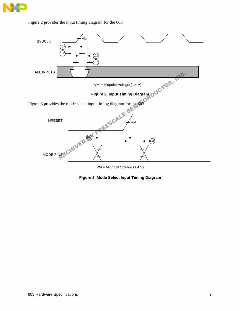
Figure 2 provides the input timing diagram for the 603.
Figure 2. Input Timing Diagram
Figure 3 provides the mode select input timing diagram for the 603.
Figure 3. Mode Select Input Timing Diagram
VMSYSCLK
ALL INPUTS
VM = Midpoint Voltage (1.4 V)
10a
10b11a
11b
MODE PINS
HRESET VM
VM = Midpoint Voltage (1.4 V)
10c11c
ARCHIVED BY FREESCALE SEMICONDUCTOR, INC.
10 603 Hardware Specifications
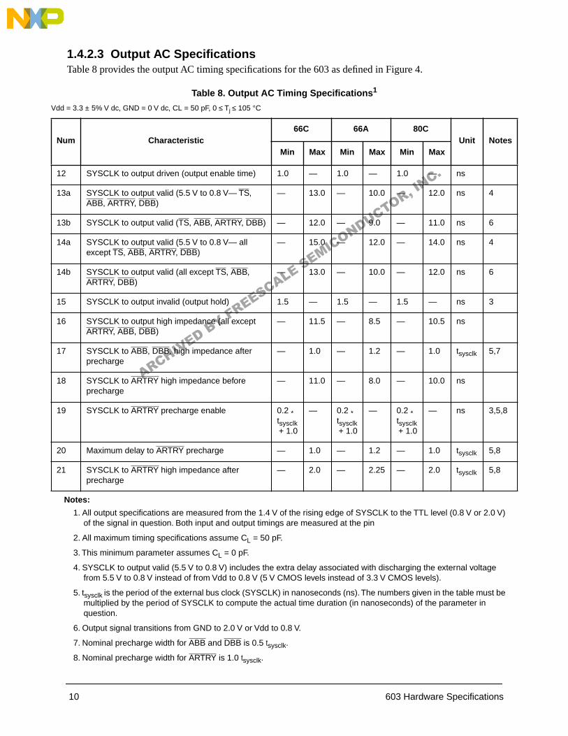
1.4.2.3 Output AC SpecificationsTable 8 provides the output AC timing specifications for the 603 as defined in Figure 4.
Table 8. Output AC Timing Specifications1
Vdd = 3.3 ± 5% V dc, GND = 0 V dc, CL = 50 pF, 0 ≤ Tj ≤ 105 °C
Num Characteristic66C 66A 80C
Unit NotesMin Max Min Max Min Max
12 SYSCLK to output driven (output enable time) 1.0 — 1.0 — 1.0 — ns
13a SYSCLK to output valid (5.5 V to 0.8 V— TS, ABB, ARTRY, DBB)
— 13.0 — 10.0 — 12.0 ns 4
13b SYSCLK to output valid (TS, ABB, ARTRY, DBB) — 12.0 — 9.0 — 11.0 ns 6
14a SYSCLK to output valid (5.5 V to 0.8 V— all except TS, ABB, ARTRY, DBB)
— 15.0 — 12.0 — 14.0 ns 4
14b SYSCLK to output valid (all except TS, ABB, ARTRY, DBB)
— 13.0 — 10.0 — 12.0 ns 6
15 SYSCLK to output invalid (output hold) 1.5 — 1.5 — 1.5 — ns 3
16 SYSCLK to output high impedance (all except ARTRY, ABB, DBB)
— 11.5 — 8.5 — 10.5 ns
17 SYSCLK to ABB, DBB, high impedance after precharge
— 1.0 — 1.2 — 1.0 tsysclk 5,7
18 SYSCLK to ARTRY high impedance before precharge
— 11.0 — 8.0 — 10.0 ns
19 SYSCLK to ARTRY precharge enable 0.2 * tsysclk
+ 1.0
— 0.2 * tsysclk
+ 1.0
— 0.2 * tsysclk
+ 1.0
— ns 3,5,8
20 Maximum delay to ARTRY precharge — 1.0 — 1.2 — 1.0 tsysclk 5,8
21 SYSCLK to ARTRY high impedance after precharge
— 2.0 — 2.25 — 2.0 tsysclk 5,8
Notes:
1. All output specifications are measured from the 1.4 V of the rising edge of SYSCLK to the TTL level (0.8 V or 2.0 V) of the signal in question. Both input and output timings are measured at the pin
2. All maximum timing specifications assume CL = 50 pF.
3. This minimum parameter assumes CL = 0 pF.
4. SYSCLK to output valid (5.5 V to 0.8 V) includes the extra delay associated with discharging the external voltage from 5.5 V to 0.8 V instead of from Vdd to 0.8 V (5 V CMOS levels instead of 3.3 V CMOS levels).
5. tsysclk is the period of the external bus clock (SYSCLK) in nanoseconds (ns). The numbers given in the table must be multiplied by the period of SYSCLK to compute the actual time duration (in nanoseconds) of the parameter in question.
6. Output signal transitions from GND to 2.0 V or Vdd to 0.8 V.
7. Nominal precharge width for ABB and DBB is 0.5 tsysclk.
8. Nominal precharge width for ARTRY is 1.0 tsysclk.
ARCHIVED BY FREESCALE SEMICONDUCTOR, INC.
603 Hardware Specifications 11
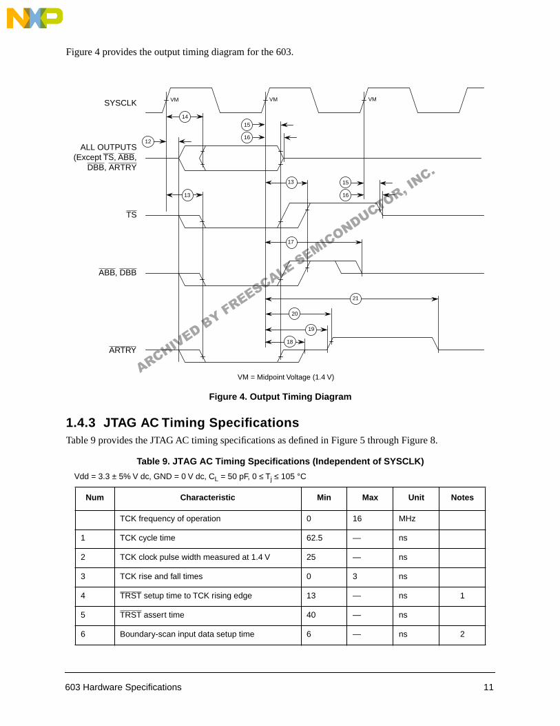
Figure 4 provides the output timing diagram for the 603.
Figure 4. Output Timing Diagram
1.4.3 JTAG AC Timing SpecificationsTable 9 provides the JTAG AC timing specifications as defined in Figure 5 through Figure 8.
Table 9. JTAG AC Timing Specifications (Independent of SYSCLK)
Vdd = 3.3 ± 5% V dc, GND = 0 V dc, CL = 50 pF, 0 ≤ Tj ≤ 105 °C
Num Characteristic Min Max Unit Notes
TCK frequency of operation 0 16 MHz
1 TCK cycle time 62.5 — ns
2 TCK clock pulse width measured at 1.4 V 25 — ns
3 TCK rise and fall times 0 3 ns
4 TRST setup time to TCK rising edge 13 — ns 1
5 TRST assert time 40 — ns
6 Boundary-scan input data setup time 6 — ns 2
SYSCLK
12
14
13
15
16
16
TS
ARTRY
ABB, DBB
VM VM
VM = Midpoint Voltage (1.4 V)
15
VM
13
20
18
17
21
19
ALL OUTPUTS(Except TS, ABB,
DBB, ARTRY
ARCHIVED BY FREESCALE SEMICONDUCTOR, INC.
12 603 Hardware Specifications
Figure 5 provides the JTAG clock input timing diagram.
Figure 5. Clock Input Timing Diagram
Figure 6 provides the TRST timing diagram.
Figure 6. TRST Timing Diagram
7 Boundary-scan input data hold time 27 — ns 2
8 TCK to output data valid 4 25 ns 3
9 TCK to output high impedance 3 24 ns 3
10 TMS, TDI data setup time 0 — ns
11 TMS, TDI data hold time 25 — ns
12 TCK to TDO data valid 4 24 ns
13 TCK to TDO high impedance 3 15 ns
Notes:
1. TRST is an asynchronous signal. The setup time is for test purposes only.
2. Non-test signal input timing with respect to TCK.
3. Non-test signal output timing with respect to TCK.
Table 9. JTAG AC Timing Specifications (Independent of SYSCLK) (Continued)
Vdd = 3.3 ± 5% V dc, GND = 0 V dc, CL = 50 pF, 0 ≤ Tj ≤ 105 °C
Num Characteristic Min Max Unit Notes
TCK
22
1
VMVMVM
33
VM = Midpoint Voltage (1.4 V)
4
5
TRST
TCKVM
ARCHIVED BY FREESCALE SEMICONDUCTOR, INC.
603 Hardware Specifications 13
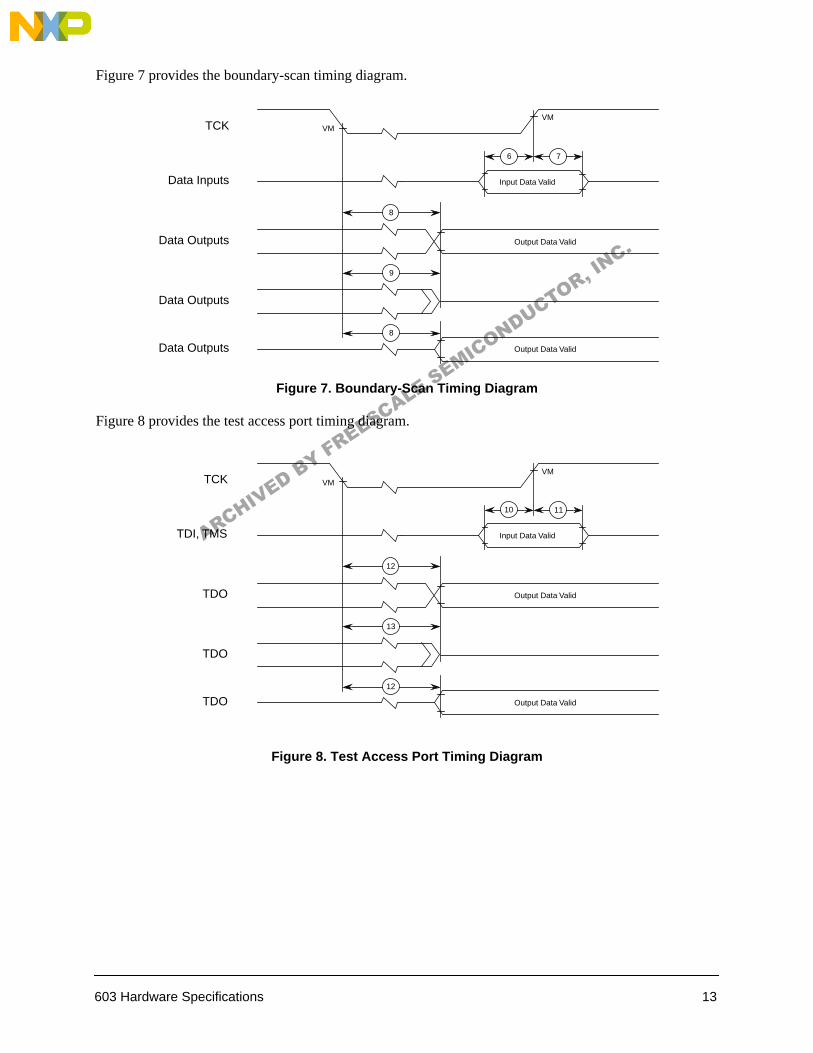
Figure 7 provides the boundary-scan timing diagram.
Figure 7. Boundary-Scan Timing Diagram
Figure 8 provides the test access port timing diagram.
Figure 8. Test Access Port Timing Diagram
6 7
Input Data Valid
8
9
8
Output Data Valid
Output Data Valid
TCK
Data Inputs
Data Outputs
Data Outputs
Data Outputs
VMVM
10 11
Input Data Valid
12
13
12
Output Data Valid
Output Data Valid
TCK
TDI, TMS
TDO
TDO
TDO
VMVM
ARCHIVED BY FREESCALE SEMICONDUCTOR, INC.
14 603 Hardware Specifications
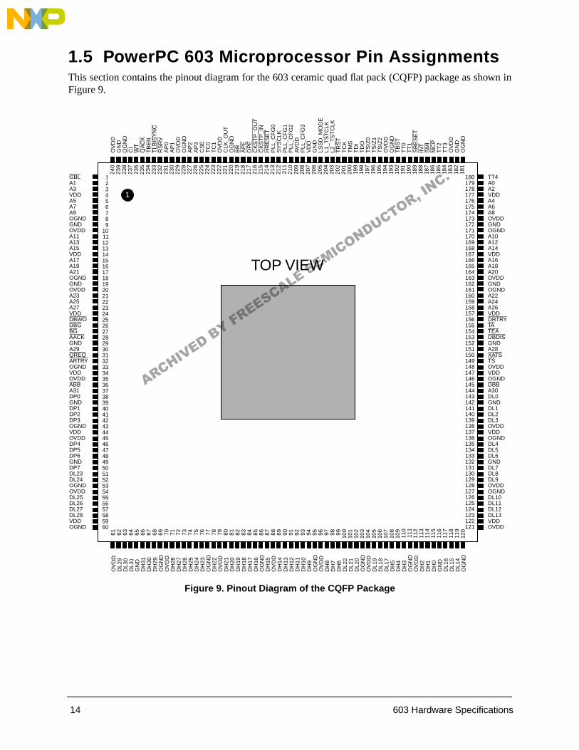
1.5 PowerPC 603 Microprocessor Pin AssignmentsThis section contains the pinout diagram for the 603 ceramic quad flat pack (CQFP) package as shown inFigure 9.
Figure 9. Pinout Diagram of the CQFP Package
GBLA1A3VDDA5A7A9OGNDGNDOVDDA11A13A15VDDA17A19A21OGNDGNDOVDDA23A25A27VDDDBWODBGBGAACKGNDA29QREQARTRYOGNDVDDOVDDABBA31DP0GNDDP1DP2DP3OGNDVDDOVDDDP4DP5DP6GNDDP7DL23DL24OGNDOVDDDL25DL26DL27DL28VDDOGND
TT4A0A2VDDA4A6A8OVDDGNDOGNDA10A12A14VDDA16A18A20OVDDGNDOGNDA22A24A26VDDDRTRYTATEADBDISGNDA28XATSTSOVDDVDDOGNDDBBA30DL0GNDDL1DL2DL3OVDDVDDOGNDDL4DL5DL6GNDDL7DL8DL9OVDDOGNDDL10DL11DL12DL13VDDOVDD
123456789
101112131415161718192021222324252627282930313233343536373839404142434445464748495051525354555657585960
180179178177176175174173172171170169168167166165164163162161160159158157156155154153152151150149148147146145144143142141140139138137136135134133132131130129128127126125124123122121
OV
DD
GN
DO
GN
DC
IW
TQ
AC
KT
BE
NT
LBIS
YN
CR
SR
VA
P0
AP
1O
VD
DO
GN
DA
P2
AP
3C
SE
TC
0T
C1
OV
DD
CLK
_OU
TO
GN
DB
RA
PE
DP
EC
KS
TP
_OU
TC
KS
TP
_IN
HR
ES
ET
PLL
_CF
G0
SY
SC
LKP
LL_C
FG
1P
LL_C
FG
2A
VD
DP
LL_C
FG
3V
DD
GN
DLS
SD
_MO
DE
L1_T
ST
CLK
L2 _
TS
TC
LKT
RS
TT
CK
TM
ST
DI
TD
OT
SIZ
0T
SIZ
1T
SIZ
2O
VD
DO
GN
DT
BS
TT
T0
TT
1S
RE
SE
TIN
TS
MI
MC
PT
T2
TT
3O
VD
DG
ND
OG
ND
240
239
238
237
236
235
234
233
232
231
230
229
228
227
226
225
224
223
222
221
220
219
218
217
216
215
214
213
212
211
210
209
208
207
206
205
204
203
202
201
200
199
198
197
196
195
194
193
192
191
190
189
188
187
186
185
184
183
182
181
OV
DD
DL2
9D
L30
DL3
1G
ND
DH
31D
H30
DH
29O
GN
DO
VD
DD
H28
DH
27D
H26
DH
25D
H24
DH
23O
GN
DD
H22
OV
DD
DH
21D
H20
DH
19D
H18
DH
17D
H16
OG
ND
DH
15O
VD
DD
H14
DH
13D
H12
DH
11D
H10
DH
9O
GN
DO
VD
DD
H8
DH
7D
H6
DL2
2D
L21
DL2
0O
GN
DO
VD
DD
L19
DL1
8D
L17
DH
5D
H4
DH
3O
GN
DO
VD
DD
H2
DH
1D
H0
GN
DD
L16
DL1
5D
L14
OG
ND
61 62 63 64 65 66 67 68 69 70 71 72 73 74 75 76 77 78 79 80 81 82 83 84 85 86 87 88 89 90 91 92 93 94 95 96 97 98 99 100
101
102
103
104
105
106
107
108
109
110
111
112
113
114
115
116
117
118
119
120
1
TOP VIEW
ARCHIVED BY FREESCALE SEMICONDUCTOR, INC.
603 Hardware Specifications 15
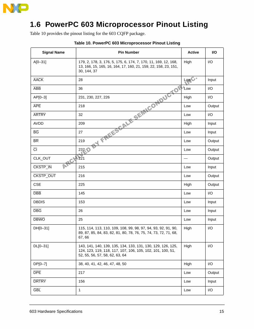
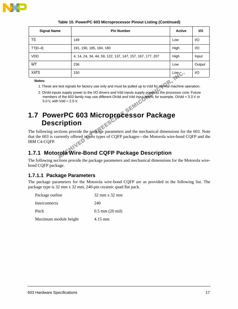
1.6 PowerPC 603 Microprocessor Pinout ListingTable 10 provides the pinout listing for the 603 CQFP package.
Table 10. PowerPC 603 Microprocessor Pinout Listing
Signal Name Pin Number Active I/O
A[0–31] 179, 2, 178, 3, 176, 5, 175, 6, 174, 7, 170, 11, 169, 12, 168, 13, 166, 15, 165, 16, 164, 17, 160, 21, 159, 22, 158, 23, 151, 30, 144, 37
High I/O
AACK 28 Low Input
ABB 36 Low I/O
AP[0–3] 231, 230, 227, 226 High I/O
APE 218 Low Output
ARTRY 32 Low I/O
AVDD 209 High Input
BG 27 Low Input
BR 219 Low Output
CI 237 Low Output
CLK_OUT 221 — Output
CKSTP_IN 215 Low Input
CKSTP_OUT 216 Low Output
CSE 225 High Output
DBB 145 Low I/O
DBDIS 153 Low Input
DBG 26 Low Input
DBWO 25 Low Input
DH[0–31] 115, 114, 113, 110, 109, 108, 99, 98, 97, 94, 93, 92, 91, 90, 89, 87, 85, 84, 83, 82, 81, 80, 78, 76, 75, 74, 73, 72, 71, 68, 67, 66
High I/O
DL[0–31] 143, 141, 140, 139, 135, 134, 133, 131, 130, 129, 126, 125, 124, 123, 119, 118, 117, 107, 106, 105, 102, 101, 100, 51, 52, 55, 56, 57, 58, 62, 63, 64
High I/O
DP[0–7] 38, 40, 41, 42, 46, 47, 48, 50 High I/O
DPE 217 Low Output
DRTRY 156 Low Input
GBL 1 Low I/O
ARCHIVED BY FREESCALE SEMICONDUCTOR, INC.
16 603 Hardware Specifications
GND 9, 19, 29, 39, 49, 65, 116, 132, 142, 152, 162, 172, 182, 206, 239
Low Input
HRESET 214 Low Input
INT 188 Low Input
LSSD_MODE1 205 Low Input
L1_TSTCLK1 204 — Input
L2_TSTCLK1 203 — Input
MCP 186 Low Input
OGND 8, 18, 33, 43, 53, 60, 69, 77, 86, 95, 103, 111, 120, 127, 136, 146, 161, 171, 181, 193, 220, 228, 238
Low Input
OVDD 10, 20, 35, 45, 54, 61, 70, 79, 88, 96, 104, 112, 121, 128, 138, 148, 163, 173, 183, 194, 222, 229, 240
High Input
PLL_CFG[0–3] 213, 211, 210, 208 High Input
QACK 235 Low Input
QREQ 31 Low Output
RSRV 232 Low Output
SMI 187 Low Input
SRESET 189 Low Input
SYSCLK 212 — Input
TA 155 Low Input
TBEN 234 High Input
TBST 192 Low I/O
TC[0–1] 224, 223 High Output
TCK 201 — Input
TDI 199 High Input
TDO 198 High Output
TEA 154 Low Input
TLBISYNC 233 Low Input
TMS 200 High Input
TRST 202 Low Input
TSIZ[0–2] 197, 196, 195 High I/O
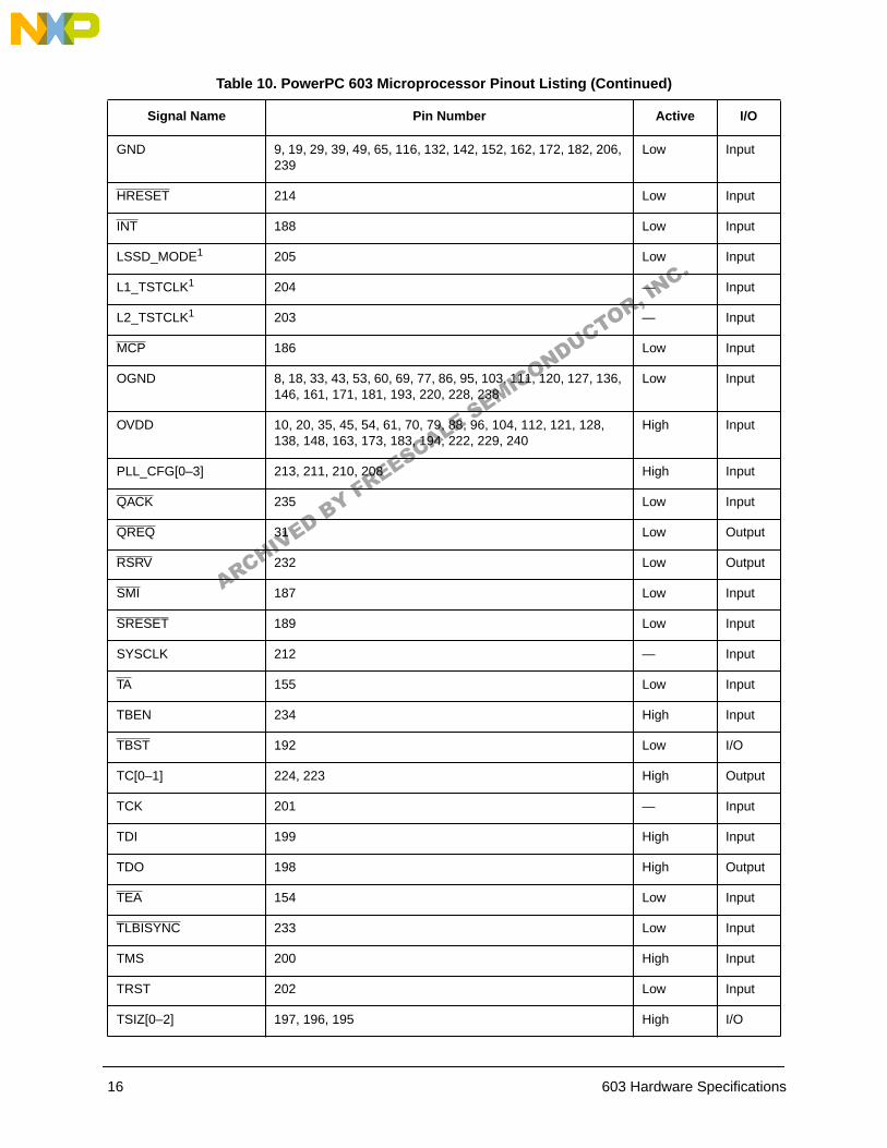
Table 10. PowerPC 603 Microprocessor Pinout Listing (Continued)
Signal Name Pin Number Active I/O
ARCHIVED BY FREESCALE SEMICONDUCTOR, INC.
603 Hardware Specifications 17
1.7 PowerPC 603 Microprocessor Package Description
The following sections provide the package parameters and the mechanical dimensions for the 603. Notethat the 603 is currently offered in two types of CQFP packages—the Motorola wire-bond CQFP and theIBM C4-CQFP.
1.7.1 Motorola Wire-Bond CQFP Package DescriptionThe following sections provide the package parameters and mechanical dimensions for the Motorola wire-bond CQFP package.
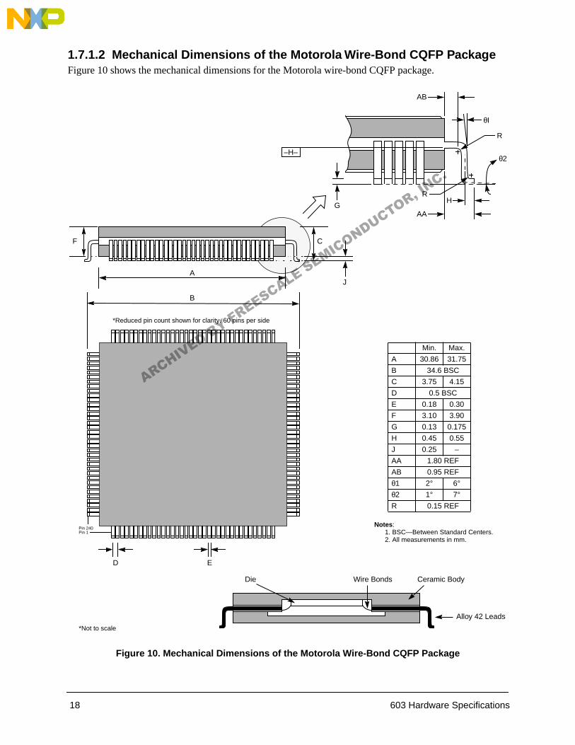
1.7.1.1 Package ParametersThe package parameters for the Motorola wire-bond CQFP are as provided in the following list. Thepackage type is 32 mm x 32 mm, 240-pin ceramic quad flat pack.
Package outline 32 mm x 32 mm
Interconnects 240
Pitch 0.5 mm (20 mil)
Maximum module height 4.15 mm
TS 149 Low I/O
TT[0–4] 191, 190, 185, 184, 180 High I/O
VDD 4, 14, 24, 34, 44, 59, 122, 137, 147, 157, 167, 177, 207 High Input
WT 236 Low Output
XATS 150 Low I/O
Notes:
1. These are test signals for factory use only and must be pulled up to Vdd for normal machine operation.
2. OVdd inputs supply power to the I/O drivers and Vdd inputs supply power to the processor core. Future members of the 603 family may use different OVdd and Vdd input levels; for example, OVdd = 3.3 V or 5.0 V, with Vdd = 2.5 V.
Table 10. PowerPC 603 Microprocessor Pinout Listing (Continued)
Signal Name Pin Number Active I/O
ARCHIVED BY FREESCALE SEMICONDUCTOR, INC.
18 603 Hardware Specifications
1.7.1.2 Mechanical Dimensions of the Motorola Wire-Bond CQFP PackageFigure 10 shows the mechanical dimensions for the Motorola wire-bond CQFP package.
Figure 10. Mechanical Dimensions of the Motorola Wire-Bond CQFP Package
*Reduced pin count shown for clarity. 60 pins per side
Min. Max.
A 30.86 31.75
B 34.6 BSC
C 3.75 4.15
D 0.5 BSC
E 0.18 0.30
F 3.10 3.90
G 0.13 0.175
H 0.45 0.55
J 0.25 –
AA 1.80 REF
AB 0.95 REF
θ1 2° 6°θ2 1° 7°R 0.15 REF
–H–
AB
θI
R
R
AA
θ2
H
Pin 240
C
A
B
Pin 1
D E
*Not to scale
G
F
J
Die Wire Bonds Ceramic Body
Alloy 42 Leads
Notes: 1. BSC—Between Standard Centers.2. All measurements in mm.
ARCHIVED BY FREESCALE SEMICONDUCTOR, INC.
603 Hardware Specifications 19
1.7.2 IBM C4-CQFP Package DescriptionThe following sections provide the package parameters and mechanical dimensions for the IBM C4-CQFPpackage.
1.7.2.1 Package ParametersThe package parameters for the IBM C4-CQFP are as provided in the following list. The package type is32 mm x 32 mm, 240-pin ceramic quad flat pack.
Package outline 32 mm x 32 mm
Interconnects 240
Pitch 0.5 mm
Lead plating Ni Au
Solder joint Sn/PB (10/90)
Lead encapsulation Epoxy
Solder-bump encapsulation Epoxy
Maximum module height 3.1 mm
Co-planarity specification 0.08 mm
Note: No solvent can be used with the C4-CQFP package. See Appendix A, “General HandlingRecommendations for the C4-CQFP Package,” for details.
ARCHIVED BY FREESCALE SEMICONDUCTOR, INC.
20 603 Hardware Specifications
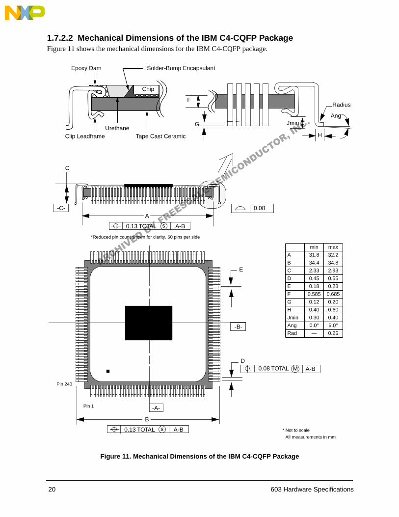
1.7.2.2 Mechanical Dimensions of the IBM C4-CQFP PackageFigure 11 shows the mechanical dimensions for the IBM C4-CQFP package.
Figure 11. Mechanical Dimensions of the IBM C4-CQFP Package
*Reduced pin count shown for clarity. 60 pins per side
min max
A 31.8 32.2
B 34.4 34.8
C 2.33 2.93
D 0.45 0.55
E 0.18 0.28
F 0.585 0.685
G 0.12 0.20
H 0.40 0.60
Jmin 0.30 0.40
Ang 0.0° 5.0°Rad — 0.25
Clip Leadframe
Chip
Tape Cast Ceramic
Epoxy Dam
Urethane
Solder-Bump Encapsulant
H
Jmin
Radius
0.08
F
G
A
B
E
0.13 TOTAL s A-B
-C-
0.13 TOTAL s A-B
0.08 TOTAL M A-BD
-A-
Pin 240
Pin 1
* Not to scale
All measurements in mm
Ang
-B-
C
ARCHIVED BY FREESCALE SEMICONDUCTOR, INC.
603 Hardware Specifications 21
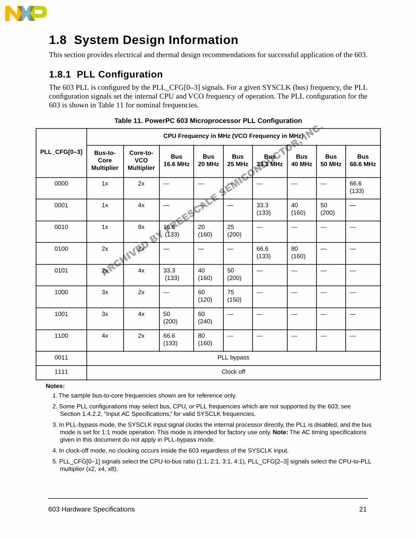
1.8 System Design InformationThis section provides electrical and thermal design recommendations for successful application of the 603.
1.8.1 PLL ConfigurationThe 603 PLL is configured by the PLL_CFG[0–3] signals. For a given SYSCLK (bus) frequency, the PLLconfiguration signals set the internal CPU and VCO frequency of operation. The PLL configuration for the603 is shown in Table 11 for nominal frequencies.
Table 11. PowerPC 603 Microprocessor PLL Configuration
PLL_CFG[0–3]
CPU Frequency in MHz (VCO Frequency in MHz)
Bus-to-Core
Multiplier
Core-to-VCO
Multiplier
Bus16.6 MHz
Bus20 MHz
Bus25 MHz
Bus33.3 MHz
Bus40 MHz
Bus50 MHz
Bus66.6 MHz
0000 1x 2x — — — — — — 66.6(133)
0001 1x 4x — — — 33.3(133)
40(160)
50(200)
—
0010 1x 8x 16.6 (133)
20(160)
25(200)
— — — —
0100 2x 2x — — — 66.6(133)
80(160)
— —
0101 2x 4x 33.3 (133)
40(160)
50(200)
— — — —
1000 3x 2x — 60(120)
75(150)
— — — —
1001 3x 4x 50(200)
60(240)
— — — — —
1100 4x 2x 66.6(133)
80(160)
— — — — —
0011 PLL bypass
1111 Clock off
Notes:
1. The sample bus-to-core frequencies shown are for reference only.
2. Some PLL configurations may select bus, CPU, or PLL frequencies which are not supported by the 603; see Section 1.4.2.2, “Input AC Specifications,” for valid SYSCLK frequencies.
3. In PLL-bypass mode, the SYSCLK input signal clocks the internal processor directly, the PLL is disabled, and the bus mode is set for 1:1 mode operation. This mode is intended for factory use only. Note: The AC timing specifications given in this document do not apply in PLL-bypass mode.
4. In clock-off mode, no clocking occurs inside the 603 regardless of the SYSCLK input.
5. PLL_CFG[0–1] signals select the CPU-to-bus ratio (1:1, 2:1, 3:1, 4:1), PLL_CFG[2–3] signals select the CPU-to-PLL multiplier (x2, x4, x8).
ARCHIVED BY FREESCALE SEMICONDUCTOR, INC.
22 603 Hardware Specifications
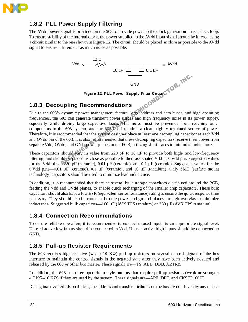
1.8.2 PLL Power Supply FilteringThe AVdd power signal is provided on the 603 to provide power to the clock generation phased-lock loop.To ensure stability of the internal clock, the power supplied to the AVdd input signal should be filtered usinga circuit similar to the one shown in Figure 12. The circuit should be placed as close as possible to the AVddsignal to ensure it filters out as much noise as possible.
Figure 12. PLL Power Supply Filter Circuit
1.8.3 Decoupling RecommendationsDue to the 603’s dynamic power management feature, large address and data buses, and high operatingfrequencies, the 603 can generate transient power surges and high frequency noise in its power supply,especially while driving large capacitive loads. This noise must be prevented from reaching othercomponents in the 603 system, and the 603 itself requires a clean, tightly regulated source of power.Therefore, it is recommended that the system designer place at least one decoupling capacitor at each Vddand OVdd pin of the 603. It is also recommended that these decoupling capacitors receive their power fromseparate Vdd, OVdd, and GND power planes in the PCB, utilizing short traces to minimize inductance.
These capacitors should vary in value from 220 pF to 10 µF to provide both high- and low-frequencyfiltering, and should be placed as close as possible to their associated Vdd or OVdd pin. Suggested valuesfor the Vdd pins—220 pF (ceramic), 0.01 µF (ceramic), and 0.1 µF (ceramic). Suggested values for theOVdd pins—0.01 µF (ceramic), 0.1 µF (ceramic), and 10 µF (tantalum). Only SMT (surface mounttechnology) capacitors should be used to minimize lead inductance.
In addition, it is recommended that there be several bulk storage capacitors distributed around the PCB,feeding the Vdd and OVdd planes, to enable quick recharging of the smaller chip capacitors. These bulkcapacitors should also have a low ESR (equivalent series resistance) rating to ensure the quick response timenecessary. They should also be connected to the power and ground planes through two vias to minimizeinductance. Suggested bulk capacitors—100 µF (AVX TPS tantalum) or 330 µF (AVX TPS tantalum).
1.8.4 Connection RecommendationsTo ensure reliable operation, it is recommended to connect unused inputs to an appropriate signal level.Unused active low inputs should be connected to Vdd. Unused active high inputs should be connected toGND.
1.8.5 Pull-up Resistor RequirementsThe 603 requires high-resistive (weak: 10 KΩ) pull-up resistors on several control signals of the businterface to maintain the control signals in the negated state after they have been actively negated andreleased by the 603 or other bus master. These signals are—TS, ABB, DBB, ARTRY.
In addition, the 603 has three open-drain style outputs that require pull-up resistors (weak or stronger:4.7 KΩ–10 KΩ) if they are used by the system. These signals are—APE, DPE, and CKSTP_OUT.
During inactive periods on the bus, the address and transfer attributes on the bus are not driven by any master
Vdd AVdd 10 Ω
10 µF 0.1 µF
GND
ARCHIVED BY FREESCALE SEMICONDUCTOR, INC.
603 Hardware Specifications 23
and may float in the high-impedance state for relatively long periods of time. Since the 603 must continuallymonitor these signals for snooping, this float condition may cause excessive power draw by the inputreceivers on the 603. It is recommended that these signals be pulled up through weak (10 KΩ) pull-upresistors or restored in some manner by the system. The snooped address and transfer attribute inputs are—A[0–31], AP[0–3], TT[0–4], TBST, TSIZ[0–2], and GBL.
The data bus input receivers are normally turned off when no read operation is in progress and do not requirepull-up resistors on the data bus.
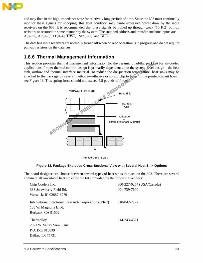
1.8.6 Thermal Management InformationThis section provides thermal management information for the ceramic quad-flat package for air-cooledapplications. Proper thermal control design is primarily dependent upon the system-level design—the heatsink, airflow and thermal interface material. To reduce the die-junction temperature, heat sinks may beattached to the package by several methods—adhesive or spring clip to holes in the printed-circuit board;see Figure 13. This spring force should not exceed 5.5 pounds of force.
Figure 13. Package Exploded Cross-Sectional View with Several Heat Sink Options
The board designer can choose between several types of heat sinks to place on the 603. There are severalcommercially-available heat sinks for the 603 provided by the following vendors:
Chip Coolers Inc. 800-227-0254 (USA/Canada)
333 Strawberry Field Rd. 401-739-7600
Warwick, RI 02887-6979
International Electronic Research Corporation (IERC) 818-842-7277
135 W. Magnolia Blvd.
Burbank, CA 91502
Thermalloy 214-243-4321
2021 W. Valley View Lane
P.O. Box 810839
Dallas, TX 75731
Adhesive
WB/CQFP Package
orThermal Interface Material
Heat Sink
Heat SinkClip
Printed-Circuit Board
ARCHIVED BY FREESCALE SEMICONDUCTOR, INC.
24 603 Hardware Specifications
Wakefield Engineering 617-245-5900
60 Audubon Rd.
Wakefield, MA 01880
Aavid Engineering 603-528-3400
One Kool Path
Laconia, NH 03247-0440
Ultimately, the final selection of an appropriate heat sink depends on many factors, such as thermalperformance at a given air velocity, spatial volume, mass, attachment method, assembly, and cost.
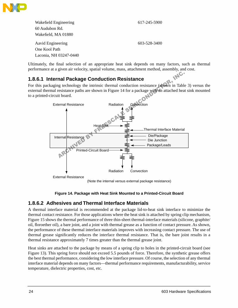
1.8.6.1 Internal Package Conduction ResistanceFor this packaging technology the intrinsic thermal conduction resistance (shown in Table 3) versus theexternal thermal resistance paths are shown in Figure 14 for a package with an attached heat sink mountedto a printed-circuit board.
Figure 14. Package with Heat Sink Mounted to a Printed-Circuit Board
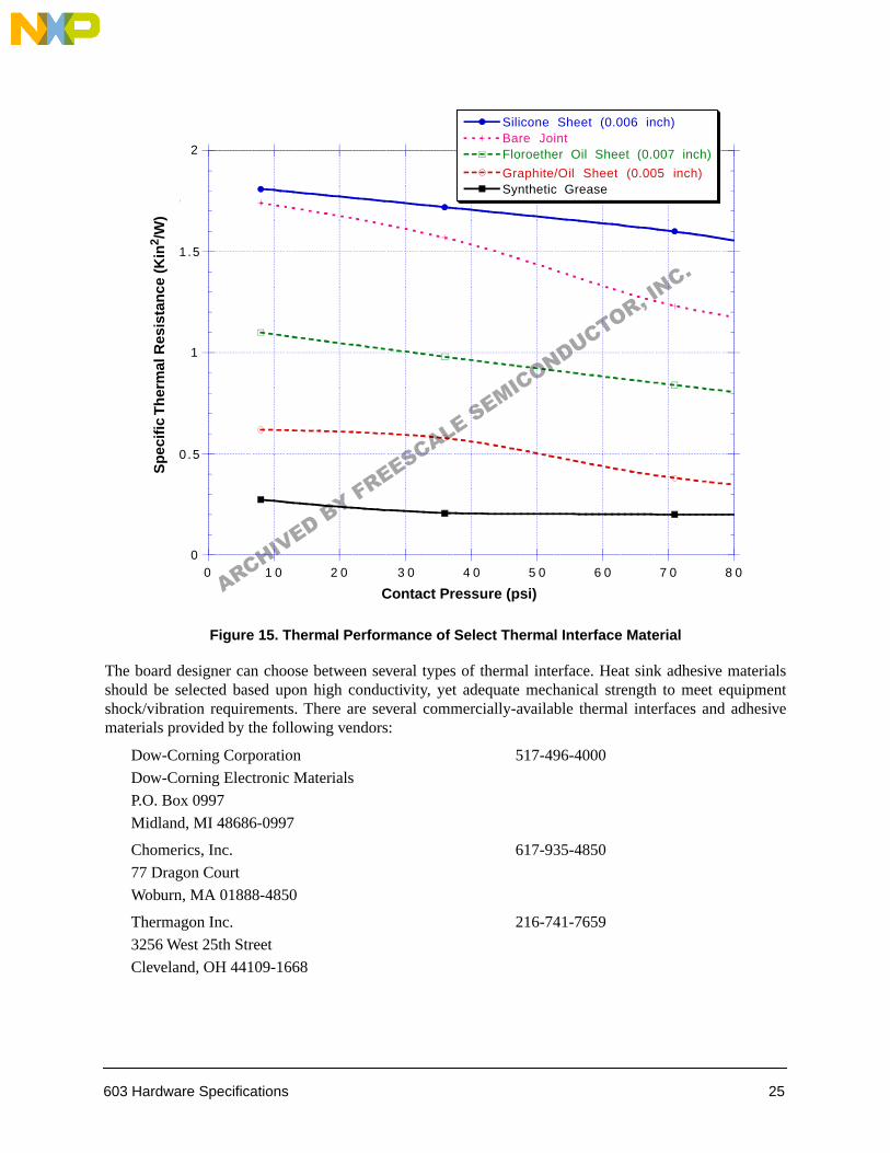
1.8.6.2 Adhesives and Thermal Interface MaterialsA thermal interface material is recommended at the package lid-to-heat sink interface to minimize thethermal contact resistance. For those applications where the heat sink is attached by spring clip mechanism,Figure 15 shows the thermal performance of three thin-sheet thermal-interface materials (silicone, graphite/oil, floroether oil), a bare joint, and a joint with thermal grease as a function of contact pressure. As shown,the performance of these thermal interface materials improves with increasing contact pressure. The use ofthermal grease significantly reduces the interface thermal resistance. That is, the bare joint results in athermal resistance approximately 7 times greater than the thermal grease joint.
Heat sinks are attached to the package by means of a spring clip to holes in the printed-circuit board (seeFigure 13). This spring force should not exceed 5.5 pounds of force. Therefore, the synthetic grease offersthe best thermal performance, considering the low interface pressure. Of course, the selection of any thermalinterface material depends on many factors—thermal performance requirements, manufacturability, servicetemperature, dielectric properties, cost, etc.
External Resistance
External Resistance
Internal Resistance
(Note the internal versus external package resistance)
Radiation Convection
Radiation Convection
Heat Sink
Printed-Circuit Board
Thermal Interface Material
Package/LeadsDie JunctionDie/Package
ARCHIVED BY FREESCALE SEMICONDUCTOR, INC.
603 Hardware Specifications 25
Figure 15. Thermal Performance of Select Thermal Interface Material
The board designer can choose between several types of thermal interface. Heat sink adhesive materialsshould be selected based upon high conductivity, yet adequate mechanical strength to meet equipmentshock/vibration requirements. There are several commercially-available thermal interfaces and adhesivematerials provided by the following vendors:
Dow-Corning Corporation 517-496-4000
Dow-Corning Electronic Materials
P.O. Box 0997
Midland, MI 48686-0997
Chomerics, Inc. 617-935-4850
77 Dragon Court
Woburn, MA 01888-4850
Thermagon Inc. 216-741-7659
3256 West 25th Street
Cleveland, OH 44109-1668
0
0.5
1
1 .5
2
0 1 0 2 0 3 0 4 0 5 0 6 0 7 0 8 0
Graphite/Oil Sheet (0.005 inch)
Silicone Sheet (0.006 inch)
Floroether Oil Sheet (0.007 inch)
Synthetic Grease
Bare Joint
Sp
ec
ific
T
he
rma
l R
es
ista
nc
e
(Kin
2/W
)
Contact Pressure (psi)Contact Pressure (psi)
Sp
ecifi
c T
her
mal
Res
ista
nce
(K
in2 /
W)
ARCHIVED BY FREESCALE SEMICONDUCTOR, INC.
26 603 Hardware Specifications
Loctite Corporation 860-571-5100
1001 Trout Brook Crossing
Rocky Hill, CT 06067
AI Technology (e.g., EG7655) 609-882-2332
1425 Lower Ferry Rd
Trent, NJ 08618
The following section provides a heat sink selection example using one of the commercially available heatsinks.
1.8.6.3 Heat Sink Selection ExampleFor preliminary heat sink sizing, the die-junction temperature can be expressed as follows:
Tj = Ta + Tr + (θjc + θint + θsa) * Pd
Where:
Tj is the die-junction temperature Ta is the inlet cabinet ambient temperatureTr is the air temperature rise within the computer cabinetθjc is the die junction-to-case thermal resistanceθint is the adhesive or interface material thermal resistanceθsa is the heat sink base-to-ambient thermal resistancePd is the power dissipated by the device
During operation the die-junction temperatures (Tj) should be maintained less than the value specified inTable 2. The temperature of the air cooling the component greatly depends upon the ambient inlet airtemperature and the air temperature rise within the electronic cabinet. An electronic cabinet inlet-airtemperature (Ta) may range from 30 to 40 °C. The air temperature rise within a cabinet (Tr) may be in therange of 5 to 10 °C. The thermal resistance of the thermal interface material (θint) is typically about 1 °C/W. Assuming a Ta of 30 °C, a Tr of 5 °C a CQFP package θjc = 2.2 °C/W, and a power consumption(Pd ) of 3.0 W, the following expression for Tj is obtained:
Die-junction temperature: Tj = 30 °C + 5 °C + (2.2 °C/W + 1.0 °C/W + Rsa) * 3.0 W
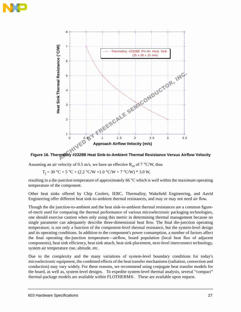
For a Thermalloy heat sink #2328B, the heat sink-to-ambient thermal resistance (Rsa) versus airflowvelocity is shown in Figure 16.
ARCHIVED BY FREESCALE SEMICONDUCTOR, INC.
603 Hardware Specifications 27
Figure 16. Thermalloy #2328B Heat Sink-to-Ambient Thermal Resistance Versus Airflow Velocity
Assuming an air velocity of 0.5 m/s, we have an effective Rsa of 7 °C/W, thus
Tj = 30 °C + 5 °C + (2.2 °C/W +1.0 °C/W + 7 °C/W) * 3.0 W,
resulting in a die-junction temperature of approximately 66 °C which is well within the maximum operatingtemperature of the component.
Other heat sinks offered by Chip Coolers, IERC, Thermalloy, Wakefield Engineering, and AavidEngineering offer different heat sink-to-ambient thermal resistances, and may or may not need air flow.
Though the die junction-to-ambient and the heat sink-to-ambient thermal resistances are a common figure-of-merit used for comparing the thermal performance of various microelectronic packaging technologies,one should exercise caution when only using this metric in determining thermal management because nosingle parameter can adequately describe three-dimensional heat flow. The final die-junction operatingtemperature, is not only a function of the component-level thermal resistance, but the system-level designand its operating conditions. In addition to the component's power consumption, a number of factors affectthe final operating die-junction temperature—airflow, board population (local heat flux of adjacentcomponents), heat sink efficiency, heat sink attach, heat sink placement, next-level interconnect technology,system air temperature rise, altitude, etc.
Due to the complexity and the many variations of system-level boundary conditions for today'smicroelectronic equipment, the combined effects of the heat transfer mechanisms (radiation, convection andconduction) may vary widely. For these reasons, we recommend using conjugate heat transfer models forthe board, as well as, system-level designs. To expedite system-level thermal analysis, several “compact”thermal-package models are available within FLOTHERM®. These are available upon request.
1
2
3
4
5
6
7
8
0 0.5 1 1.5 2 2.5 3 3.5
Thermalloy #2328B Pin-fin Heat Sink (25 x 28 x 15 mm)
Hea
t S
ink
Th
erm
al R
esis
tan
ce
(°C
/W)
Approach Airflow Velocity (m/s)Approach Airflow Velocity (m/s)
Hea
t S
ink
Th
erm
al R
esis
tan
ce (
°C/W
)
ARCHIVED BY FREESCALE SEMICONDUCTOR, INC.
28 603 Hardware Specifications
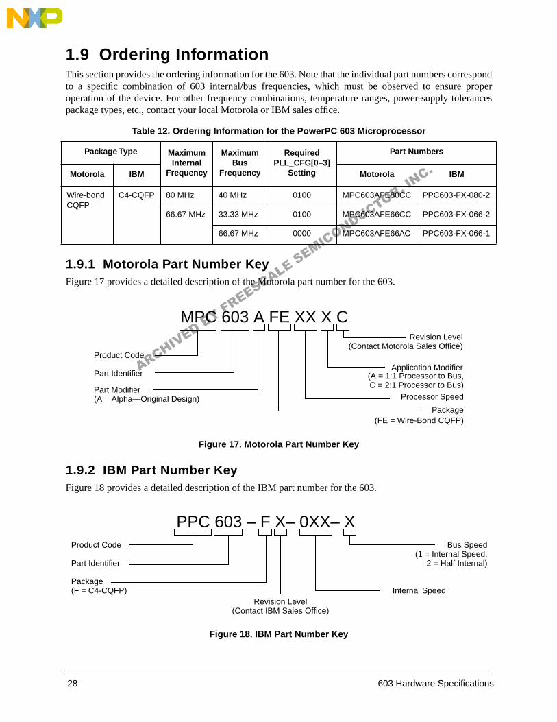
1.9 Ordering InformationThis section provides the ordering information for the 603. Note that the individual part numbers correspondto a specific combination of 603 internal/bus frequencies, which must be observed to ensure properoperation of the device. For other frequency combinations, temperature ranges, power-supply tolerancespackage types, etc., contact your local Motorola or IBM sales office.
1.9.1 Motorola Part Number KeyFigure 17 provides a detailed description of the Motorola part number for the 603.
Figure 17. Motorola Part Number Key
1.9.2 IBM Part Number KeyFigure 18 provides a detailed description of the IBM part number for the 603.
Figure 18. IBM Part Number Key
Table 12. Ordering Information for the PowerPC 603 Microprocessor
Package Type Maximum Internal
Frequency
Maximum Bus
Frequency
Required PLL_CFG[0–3]
Setting
Part Numbers
Motorola IBM Motorola IBM
Wire-bond CQFP
C4-CQFP 80 MHz 40 MHz 0100 MPC603AFE80CC PPC603-FX-080-2
66.67 MHz 33.33 MHz 0100 MPC603AFE66CC PPC603-FX-066-2
66.67 MHz 0000 MPC603AFE66AC PPC603-FX-066-1
MPC 603 A FE XX X C
Product Code
Part Identifier
Part Modifier
Application Modifier
Processor Speed
Package(A = Alpha—Original Design)
(FE = Wire-Bond CQFP)
(A = 1:1 Processor to Bus,C = 2:1 Processor to Bus)
Revision Level(Contact Motorola Sales Office)
(F = C4-CQFP)
Part Identifier
PPC 603 – F X– 0XX– X
Package
Revision Level
Bus Speed
Internal Speed
(Contact IBM Sales Office)
(1 = Internal Speed,2 = Half Internal)
Product Code
ARCHIVED BY FREESCALE SEMICONDUCTOR, INC.

603 Hardware Specifications 29
Appendix AGeneral Handling Recommendations for the
C4-CQFP PackageThe following list provides a few guidelines for package handling:
• Handle the electrostatic discharge sensitive (ESD) package with care before, during, and after processing.
• Do not apply any load to exceed 3 Kg after assembly.
• Components should not be hot-dip tinned.
• The package encapsulation is an acrylated urethane. Use adequate ventilation (local exhaust) for all elevated temperature processes.
The package parameters are as follows:
Heat sink adhesive AIEG-7655
IBM reference drawing 99F4869
Test socket Yamaichi QFP-PO 0.5-240P
Signal 165
Power/ground 75
Total 240
A.1 Package Environmental, Operation, Shipment, and Storage Requirements
The environmental, operation, shipment, and storage requirements are as follows:
• Make sure that the package is suitable for continuous operation under business office environments.
— Operating environment: 10 °C to 40 °C, 8% to 80% relative humidity
— Storage environment: 1 °C to 60 °C, up to 80% relative humidity
— Shipping environment: 40 °C to 60 °C, 5% to 100% relative humidity
• This component is qualified to meet JEDEC moisture Class 2.
After expiration of shelf life, packages may be baked at 120 °C (+10/–5 °C) for 4 hours minimum and then be used or repackaged. Shelf life is as specified by JEDEC for moisture Class 2 components.
A.2 Card Assembly RecommendationsThis section provides recommendations for card assembly process. Follow these guidelines for cardassembly.
• This component is supported for aqueous, IR, convection reflow, and vapor phase card assembly processes.
• The temperature of packages should not exceed 220 °C for longer than 5 minutes.
• The package entering a cleaning cycle must not be exposed to temperature greater than that occurring during solder reflow or hot air exposure.
• It is not recommended to re-attach a package that is removed after card assembly.
ARCHIVED BY FREESCALE SEMICONDUCTOR, INC.
30 603 Hardware Specifications
During the card assembly process, no solvent can be used with the C4FP, and no more than 3 Kg of forcemust be applied normal to the top of the package prior to, during, or after card assembly. Other details ofthe card assembly process follow:
Solder paste Either water soluble (for example, Alpha 1208) or no clean
Solder stencil thickness 0.152 mm
Solder stencil aperature Width reduced to 0.03 mm from the board pad width
Placement tool Panasonic MPA3 or equivalent
Solder reflow Infrared, convection, or vapor phase
Solder reflow profile Infrared and/or convection• Average ramp-up—0.48 to 1.8 °C/second
• Time above 183 °C—45 to 145 seconds
• Minimum lead temperature—200 °C
• Maximum lead temperature—240 °C
• Maximum C4FP temperature—245 °C
Vapor phase• Preheat (board)—60 °C to 150 °C
• Time above 183 °C—60 to 145 seconds
• Minimum lead temperature—200 °C
• Maximum C4FP temperature—220 °C
• Egress temperature—below 150 °C
Clean after reflow De-ionized (D.I.) water if water-soluble paste is used• Cleaner requirements—conveyorized, in-line
• Minimum of four washing chambers
— Pre-clean chamber: top and bottom sprays, minimum top-side pressure of 25 psig, water temperature of 70 °C minimum, dwell time of 24 seconds minimum, water is not re-used, water flow rate of 30 liters/minute.
— Wash chamber #1: top and bottom sprays, minimum top-side pressure of 48 psig, minimum bottom-side pressure of 44 psig, water temperature of 62.5 °C (±2.5 °C), dwell time of 48 seconds minimum, water flow rate of 350 liters/minute.
— Wash chamber #2: top and bottom sprays, minimum top-side pressure of 32 psig, minimum bottom-side pressure of 28 psig, water temperature of 72.5 °C (±2.5 °C), dwell time of 48 seconds minimum, water flow rate of 325 liters/minute.
— Final rinse chamber: top and bottom sprays, minimum top-side pressure of 25 psig, water temperature of 72.5 °C minimum, dwell time of 24 seconds minimum, water flow rate of 30 liters/minute.
• No cleaning required if “no clean solder paste” is used
Touch-up and repair Water soluble (for example, Kester 450) or No Clean Flux
C4FP removal Hot air rework
C4FP replace Hand solder
ARCHIVED BY FREESCALE SEMICONDUCTOR, INC.
Information in this document is provided solely to enable system and software implementers to use PowerPC microprocessors. There are no express orimplied copyright or patent licenses granted hereunder by Motorola or IBM to design, modify the design of, or fabricate circuits based on the information inthis document.
The PowerPC 603 microprocessor embodies the intellectual property of Motorola and of IBM. However, neither Motorola nor IBM assumes any responsibilityor liability as to any aspects of the performance, operation, or other attributes of the microprocessor as marketed by the other party or by any third party. NeitherMotorola nor IBM is to be considered an agent or representative of the other, and neither has assumed, created, or granted hereby any right or authority to theother, or to any third party, to assume or create any express or implied obligations on its behalf. Information such as errata sheets and data sheets, as well assales terms and conditions such as prices, schedules, and support, for the product may vary as between parties selling the product. Accordingly, customerswishing to learn more information about the products as marketed by a given party should contact that party.
Both Motorola and IBM reserve the right to modify this document and/or any of the products as described herein without further notice. NOTHING IN THISDOCUMENT, NOR IN ANY OF THE ERRATA SHEETS, DATA SHEETS, AND OTHER SUPPORTING DOCUMENTATION, SHALL BE INTERPRETED AS THECONVEYANCE BY MOTOROLA OR IBM OF AN EXPRESS WARRANTY OF ANY KIND OR IMPLIED WARRANTY, REPRESENTATION, OR GUARANTEEREGARDING THE MERCHANTABILITY OR FITNESS OF THE PRODUCTS FOR ANY PARTICULAR PURPOSE. Neither Motorola nor IBM assumes anyliability or obligation for damages of any kind arising out of the application or use of these materials. Any warranty or other obligations as to the products describedherein shall be undertaken solely by the marketing party to the customer, under a separate sale agreement between the marketing party and the customer. In theabsence of such an agreement, no liability is assumed by Motorola, IBM, or the marketing party for any damages, actual or otherwise.
“Typical” parameters can and do vary in different applications. All operating parameters, including “Typicals,” must be validated for each customer application bycustomer’s technical experts. Neither Motorola nor IBM convey any license under their respective intellectual property rights nor the rights of others. NeitherMotorola nor IBM makes any claim, warranty, or representation, express or implied, that the products described in this document are designed, intended, orauthorized for use as components in systems intended for surgical implant into the body, or other applications intended to support or sustain life, or for any otherapplication in which the failure of the product could create a situation where personal injury or death may occur. Should customer purchase or use the productsfor any such unintended or unauthorized application, customer shall indemnify and hold Motorola and IBM and their respective officers, employees, subsidiaries,affiliates, and distributors harmless against all claims, costs, damages, and expenses, and reasonable attorney’s fees arising out of, directly or indirectly, any claimof personal injury or death associated with such unintended or unauthorized use, even if such claim alleges that Motorola or IBM was negligent regarding thedesign or manufacture of the part.
Motorola and are registered trademarks of Motorola, Inc. Motorola, Inc. is an Equal Opportunity/Affirmative Action Employer.
IBM, the IBM logo, and IBM Microelectronics are trademarks of International Business Machines Corporation.The PowerPC name, the PowerPC logotype, and PowerPC 603 are trademarks of International Business Machines Corporation, used by Motorola under licensefrom International Business Machines Corporation. International Business Machines Corporation is an Equal Opportunity/Affirmative Action Employer.
International Business Machines Corporation:IBM Microelectronics Division, 1580 Route 52, Bldg. 504, HopewellJunction, NY 12533-6531; Tel. (800) PowerPCWorld Wide Web Address: http://www.chips.ibm.com/products/ppc
http://www.ibm.com
Motorola Literature Distribution Centers:USA/EUROPE: Motorola Literature Distribution; P.O. Box 5405; Denver, Colorado 80217; Tel.: 1-800-441-2447 or (303) 675-2140JAPAN: Nippon Motorola Ltd.; Tatsumi-SPD-JLDC, Toshikatsu Otsuki, 6F Seibu-Butsuryu-Center, 3-14-2 Tatsumi Koto-Ku, Tokyo 135, Japan; Tel.: 81-3-3521-8315ASIA/PACIFC: Motorola Semiconductors H.K. Ltd.; 8B Tai Ping Industrial Park, 51 TingKok Road, Tai Po, N.T., Hong Kong; Tel.: 852-26629298
Technical Information: Motorola Inc. SPS Customer Support Center; (800) 521-6274.Document Comments: FAX (512) 891-2638, Attn: RISC Applications Engineering.
Mfax is a trademark of Motorola, Inc.
ARCHIVED BY FREESCALE SEMICONDUCTOR, INC.