PowerPC 750TM SCM RISC Microprocessor for the · PDF filePowerPC 750TM SCM RISC...
46
PowerPC 750 TM SCM RISC Microprocessor for the PID8p-750 Version 2.0 09/30/1999 IBM Microelectronics Division
Transcript of PowerPC 750TM SCM RISC Microprocessor for the · PDF filePowerPC 750TM SCM RISC...
PowerPC 750 TM SCM RISC Microprocessorfor the PID8p-750
Version 2.0
09/30/1999
IBM Microelectronics Division
Notices
Before using this information and the product it supports, be sure to read the general information on theback cover of this book.
Trademarks
The following are trademarks of International Business Machines Corporation in the United States, orother countries, or both:
IBM IBM Logo PowerPCAIX PowerPC 750
Preliminary Edition (Version 2.0, 09/30/1999)This document is the preliminary edition of PowerPC 750TM SCM RISC Microprocessor for the PID8p-750.
This document contains information on a new product under development by IBM. IBM reserves theright to change or discontinue this product without notice.
© International Business Machines Corporation1999.All rights reserved.
PowerPC 750 SCM RISC MicroprocessorPreliminary Copy PID8p-750
Preface . . . . . . . . . . . . . . . . . . . . . . . . . . . . . . . . . . . . . . . . . . . . . . . . . . 1
Overview . . . . . . . . . . . . . . . . . . . . . . . . . . . . . . . . . . . . . . . . . . . . . . . . 2
Features . . . . . . . . . . . . . . . . . . . . . . . . . . . . . . . . . . . . . . . . . . . . . . . . . 3
General Parameters . . . . . . . . . . . . . . . . . . . . . . . . . . . . . . . . . . . . . . . . 5
Electrical and Thermal Characteristics . . . . . . . . . . . . . . . . . . . . . . . . . 6
AC Electrical Characteristics . . . . . . . . . . . . . . . . . . . . . . . . . . . . . . . . . 10
IEEE 1149.1 AC Timing Specifications . . . . . . . . . . . . . . . . . . . . . . . . . 20
PowerPC PID8p-750 Microprocessor Pin Assignments . . . . . . . . . . . . 23
PowerPC PID8p-750 Microprocessor Pinout Listings . . . . . . . . . . . . . . 24
PowerPC PID8p-750 Microprocessor Package Description . . . . . . . . . 27
System Design Information . . . . . . . . . . . . . . . . . . . . . . . . . . . . . . . . . . 30
Ordering Information . . . . . . . . . . . . . . . . . . . . . . . . . . . . . . . . . . . . . . . 40
Processor Version Register (PVR) . . . . . . . . . . . . . . . . . . . . . . . . . . . . 40
9/30/99 Version 2.0 Datasheet Page iii
PowerPC 750 SCM RISC MicroprocessorPID8p-750 Preliminary Copy
Page iv Version 2.0 Datasheet 9/30/99
PowerPC 750 SCM RISC Microprocessor
Preliminary Copy PID8p-750
Preface
The PowerPC PID8p-750 microprocessor is an implementation of the PowerPCTM family of reduced instruc-tion set computer (RISC) microprocessors. In this document, the term “PID8p-750” is used as an abbreviationfor the phrase “PowerPC 750 SCM RISC Microprocessor Family: PID8p-750 microprocessor.”
This document contains pertinent physical characteristics of the PID8p-750 Single Chip Modules (SCM) andcovers the following topics:
Topic
• Overview (page 2)
• Features (page 3)
• General Parameters (page 5)
• Electrical and Thermal Characteristics (page 6)
• PowerPC PID8p-750 Microprocessor Pin Assignments (page 23)
• PowerPC PID8p-750 Microprocessor Pinout Listings (page 24)
• PowerPC PID8p-750 Microprocessor Package Description (page 27)
• System Design Information (page 30)
• Ordering Information (page 40)
New features/deletions for rev level dd3.x:
• Selectable I/O voltages on 60X bus (pin W1) and L2 bus (pin A19). See Table , “Recommended OperatingConditions1,2,3,” on page 6. Older revs must leave these pins “no connect” or “tied high” for 3.3v I/Os. ACtimings are the same for all I/O voltage modes unless otherwise noted. The 1.8v I/O is selected by tyingthe I/O select pin to ground. If a pull down resistor is necessary, the resistor value must be no more than10 ohms.
• 60X bus to core frequency now also supports the 10x ratio. See Table , “PID8p-750 Microprocessor PLLConfiguration,” on page 30 for how to set this ratio.
• Extra output hold on the 60X bus by L2_TSTCLK pin tied low is no longer available. The L2_TSTCLK pinmust now be tied to OVDD for normal operation. See Table , “60X Bus Output AC Timing Specifications1,”on page 13.
9/30/99 Version 2.0 Datasheet Page 1
PowerPC 750 SCM RISC MicroprocessorPID8p-750 Preliminary Copy
Overview
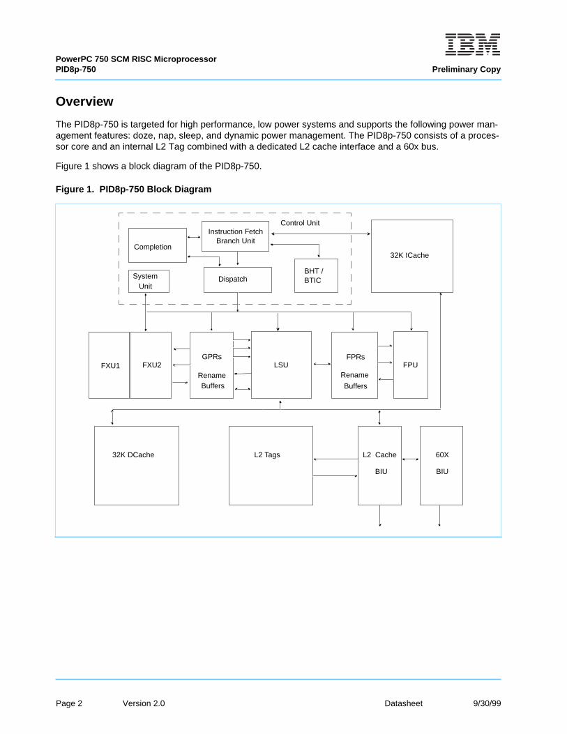
The PID8p-750 is targeted for high performance, low power systems and supports the following power man-agement features: doze, nap, sleep, and dynamic power management. The PID8p-750 consists of a proces-sor core and an internal L2 Tag combined with a dedicated L2 cache interface and a 60x bus.
Figure 1 shows a block diagram of the PID8p-750.
Figure 1. PID8p-750 Block Diagram
FXU2GPRs
LSU FPU
Instruction Fetch
System
Completion
Rename Buffers
Unit
32K ICache
32K DCache
BHT /
BIUBIU
60XL2 Cache
FXU1
L2 Tags
Dispatch
Branch Unit
BTIC
Control Unit
FPRs
Rename
Buffers
Page 2 Version 2.0 Datasheet 9/30/99
PowerPC 750 SCM RISC MicroprocessorPreliminary Copy PID8p-750
Features
This section summarizes features of the PID8p-750’s implementation of the PowerPC architecture. Major fea-tures of the PID8p-750 are as follows.
• Branch processing unit- Four instructions fetched per clock.- One branch processed per cycle (plus resolving 2 speculations).- Up to 1 speculative stream in execution, 1 additional speculative stream in fetch.- 512-entry branch history table (BHT) for dynamic prediction.- 64-entry, 4-way set associative branch target instruction cache (BTIC) for eliminating branch delay
slots.
• Dispatch unit- Full hardware detection of dependencies (resolved in the execution units).- Dispatch two instructions to six independent units (system, branch, load/store, fixed-point unit 1,
fixed-point unit 2, or floating-point).- Serialization control (predispatch, postdispatch, execution, serialization).
• Decode- Register file access.- Forwarding control.- Partial instruction decode.
• Load/store unit- One cycle load or store cache access (byte, half-word, word, double-word).- Effective address generation.- Hits under misses (one outstanding miss).- Single-cycle misaligned access within double word boundary.- Alignment, zero padding, sign extend for integer register file.- Floating-point internal format conversion (alignment, normalization).- Sequencing for load/store multiples and string operations.- Store gathering.- Cache and TLB instructions.- Big and little-endian byte addressing supported.- Misaligned little-endian support in hardware.
• Fixed-point units- Fixed-point unit 1 (FXU1); multiply, divide, shift, rotate, arithmetic, logical.- Fixed-point unit 2 (FXU2); shift, rotate, arithmetic, logical.- Single-cycle arithmetic, shift, rotate, logical.- Multiply and divide support (multi-cycle).- Early out multiply.
• Floating-point unit- Support for IEEE-754 standard single- and double-precision floating-point arithmetic.- 3 cycle latency, 1 cycle throughput, single-precision multiply-add.- 3 cycle latency, 1 cycle throughput, double-precision add.- 4 cycle latency, 2 cycle throughput, double-precision multiply-add.- Hardware support for divide.- Hardware support for denormalized numbers.- Time deterministic non-IEEE mode.
• System unit- Executes CR logical instructions and miscellaneous system instructions.
9/30/99 Version 2.0 Datasheet Page 3
PowerPC 750 SCM RISC MicroprocessorPID8p-750 Preliminary Copy
- Special register transfer instructions.
• Cache structure- 32K, 32-byte line, 8-way set associative instruction cache.- 32K, 32-byte line, 8-way set associative data cache.- Single-cycle cache access.- Pseudo-LRU replacement.- Copy-back or write-through data cache (on a page per page basis).- Supports all PowerPC memory coherency modes.- Non-blocking instruction and data cache (one outstanding miss under hits).- No snooping of instruction cache.
• Memory management unit- 128 entry, 2-way set associative instruction TLB.- 128 entry, 2-way set associative data TLB.- Hardware reload for TLB's.- 4 instruction BAT's and 4 data BATs.- Virtual memory support for up to 4 exabytes (252) virtual memory.- Real memory support for up to 4 gigabytes (232) of physical memory.
• Level 2 (L2) cache interface- Internal L2 cache controller and 4K-entry tags; external data SRAMs.- 256K, 512K, and 1 Mbyte 2-way set associative L2 cache support.- Copy-back or write-through data cache (on a page basis, or for all L2).- 64-byte (256K/512K) and 128-byte (l-Mbyte) sectored line size.- Supports flow-through (reg-buf) synchronous burst SRAMs, pipelined (reg-reg) synchronous burst
SRAMs, and pipelined (reg-reg) late-write synchronous burst SRAMs.- Design supports Core-to-L2 frequency divisors of ÷1, ÷1.5, ÷2, ÷2.5, and ÷3. However, this specifica-
tion supports the L2 frequency range specified in Section “L2 Clock AC Specifications,” on page 15.For higher L2 frequencies not supported in this document, please contact your IBM marketing repre-sentative.
• Bus interface- Compatible with 60x processor interface.- 32-bit address bus.- 64-bit data bus.- Bus-to-core frequency multipliers of 3x, 3.5x, 4x, 4.5x, 5x, 5.5x, 6x, 6.5x, 7x, 7.5x, 8x and 10x sup-
ported (10x on rev level dd3.x only).
• Integrated power management- Low-power 2.0/3.3V design.- Three static power saving modes: doze, nap, and sleep.- Automatic dynamic power reduction when internal functional units are idle.
• Integrated Thermal Management Assist Unit- On-chip thermal sensor and control logic.- Thermal Management Interrupt for software regulation of junction temperature.
• Testability- LSSD scan design.- JTAG interface.
• Reliability and serviceability–Parity checking on 60x and L2 cache buses
Page 4 Version 2.0 Datasheet 9/30/99
PowerPC 750 SCM RISC MicroprocessorPreliminary Copy PID8p-750
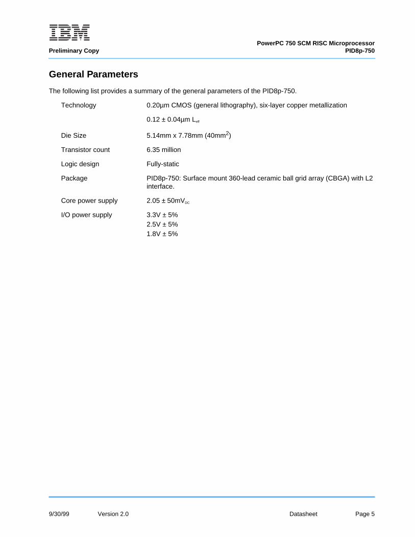
General Parameters
The following list provides a summary of the general parameters of the PID8p-750.
Technology 0.20µm CMOS (general lithography), six-layer copper metallization
0.12 ± 0.04µm Leff
Die Size 5.14mm x 7.78mm (40mm2)
Transistor count 6.35 million
Logic design Fully-static
Package PID8p-750: Surface mount 360-lead ceramic ball grid array (CBGA) with L2interface.
Core power supply 2.05 ± 50mVDC
I/O power supply 3.3V ± 5%2.5V ± 5%1.8V ± 5%
9/30/99 Version 2.0 Datasheet Page 5
PowerPC 750 SCM RISC MicroprocessorPID8p-750 Preliminary Copy
Electrical and Thermal Characteristics
This section provides both AC and DC electrical specifications and thermal characteristics for the PID8p-750.
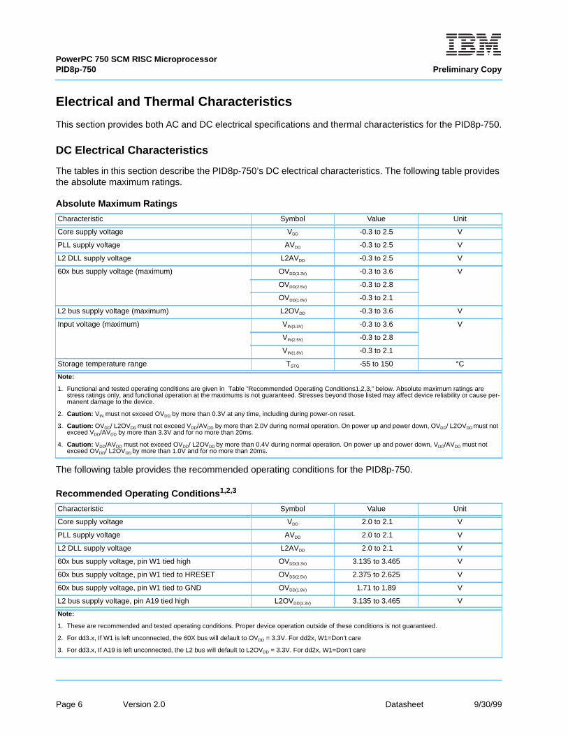
DC Electrical Characteristics
The tables in this section describe the PID8p-750’s DC electrical characteristics. The following table providesthe absolute maximum ratings.
The following table provides the recommended operating conditions for the PID8p-750.
Absolute Maximum Ratings
Characteristic Symbol Value Unit
Core supply voltage VDD -0.3 to 2.5 V
PLL supply voltage AVDD -0.3 to 2.5 V
L2 DLL supply voltage L2AVDD -0.3 to 2.5 V
60x bus supply voltage (maximum) OVDD(3.3V) -0.3 to 3.6 V
OVDD(2.5V) -0.3 to 2.8
OVDD(1.8V) -0.3 to 2.1
L2 bus supply voltage (maximum) L2OVDD -0.3 to 3.6 V
Input voltage (maximum) VIN(3.3V) -0.3 to 3.6 V
VIN(2.5V) -0.3 to 2.8
VIN(1.8V) -0.3 to 2.1
Storage temperature range TSTG -55 to 150 °C
Note:
1. Functional and tested operating conditions are given in Table ”Recommended Operating Conditions1,2,3,” below. Absolute maximum ratings arestress ratings only, and functional operation at the maximums is not guaranteed. Stresses beyond those listed may affect device reliability or cause per-manent damage to the device.
2. Caution: VIN must not exceed OVDD by more than 0.3V at any time, including during power-on reset.
3. Caution: OVDD/ L2OVDD must not exceed VDD/AVDD by more than 2.0V during normal operation. On power up and power down, OVDD/ L2OVDD must notexceed VDD/AVDD by more than 3.3V and for no more than 20ms.
4. Caution: VDD/AVDD must not exceed OVDD/ L2OVDD by more than 0.4V during normal operation. On power up and power down, VDD/AVDD must notexceed OVDD/ L2OVDD by more than 1.0V and for no more than 20ms.
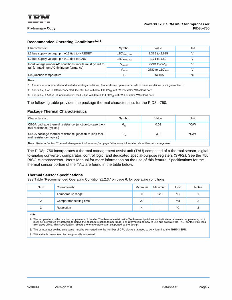
Recommended Operating Conditions 1,2,3
Characteristic Symbol Value Unit
Core supply voltage VDD 2.0 to 2.1 V
PLL supply voltage AVDD 2.0 to 2.1 V
L2 DLL supply voltage L2AVDD 2.0 to 2.1 V
60x bus supply voltage, pin W1 tied high OVDD(3.3V) 3.135 to 3.465 V
60x bus supply voltage, pin W1 tied to HRESET OVDD(2.5V) 2.375 to 2.625 V
60x bus supply voltage, pin W1 tied to GND OVDD(1.8V) 1.71 to 1.89 V
L2 bus supply voltage, pin A19 tied high L2OVDD(3.3V) 3.135 to 3.465 V
Note:
1. These are recommended and tested operating conditions. Proper device operation outside of these conditions is not guaranteed.
2. For dd3.x, If W1 is left unconnected, the 60X bus will default to OVDD = 3.3V. For dd2x, W1=Don’t care
3. For dd3.x, If A19 is left unconnected, the L2 bus will default to L2OVDD = 3.3V. For dd2x, W1=Don’t care
Page 6 Version 2.0 Datasheet 9/30/99
PowerPC 750 SCM RISC MicroprocessorPreliminary Copy PID8p-750
The following table provides the package thermal characteristics for the PID8p-750.
The PID8p-750 incorporates a thermal management assist unit (TAU) composed of a thermal sensor, digital-to-analog converter, comparator, control logic, and dedicated special-purpose registers (SPRs). See the 750RISC Microprocessor User’s Manual for more information on the use of this feature. Specifications for thethermal sensor portion of the TAU are found in the table below.
L2 bus supply voltage, pin A19 tied to HRESET L2OVDD(2.5V) 2.375 to 2.625 V
L2 bus supply voltage, pin A19 tied to GND L2OVDD(1.8V) 1.71 to 1.89 V
Input voltage (under AC conditions, inputs must go rail torail for maximum AC timing performance)
VIN(60X) GND to OVDD V
VIN(L2) GND to L2OVDD V
Die-junction temperature TJ 0 to 105 °C
Package Thermal Characteristics
Characteristic Symbol Value Unit
CBGA package thermal resistance, junction-to-case ther-mal resistance (typical)
θJC
0.03 °C/W
CBGA package thermal resistance, junction-to-lead ther-mal resistance (typical)
θJB
3.8 °C/W
Note: Refer to Section “Thermal Management Information,” on page 34 for more information about thermal management.
Thermal Sensor SpecificationsSee Table “Recommended Operating Conditions1,2,3,” on page 6, for operating conditions.
Num Characteristic Minimum Maximum Unit Notes
1 Temperature range 0 128 °C 1
2 Comparator settling time 20 — ms 2
3 Resolution 4 — °C 3
Note:
1. The temperature is the junction temperature of the die. The thermal assist unit's (TAU) raw output does not indicate an absolute temperature, but itmust be interpreted by software to derive the absolute junction temperature. For information on how to use and calibrate the TAU, contact your localIBM sales office. This specification reflects the temperature span supported by the design.
2. The comparator settling time value must be converted into the number of CPU clocks that need to be written into the THRM3 SPR.
3. This value is guaranteed by design and is not tested.
Recommended Operating Conditions 1,2,3
Characteristic Symbol Value Unit
Note:
1. These are recommended and tested operating conditions. Proper device operation outside of these conditions is not guaranteed.
2. For dd3.x, If W1 is left unconnected, the 60X bus will default to OVDD = 3.3V. For dd2x, W1=Don’t care
3. For dd3.x, If A19 is left unconnected, the L2 bus will default to L2OVDD = 3.3V. For dd2x, W1=Don’t care
9/30/99 Version 2.0 Datasheet Page 7
PowerPC 750 SCM RISC MicroprocessorPID8p-750 Preliminary Copy
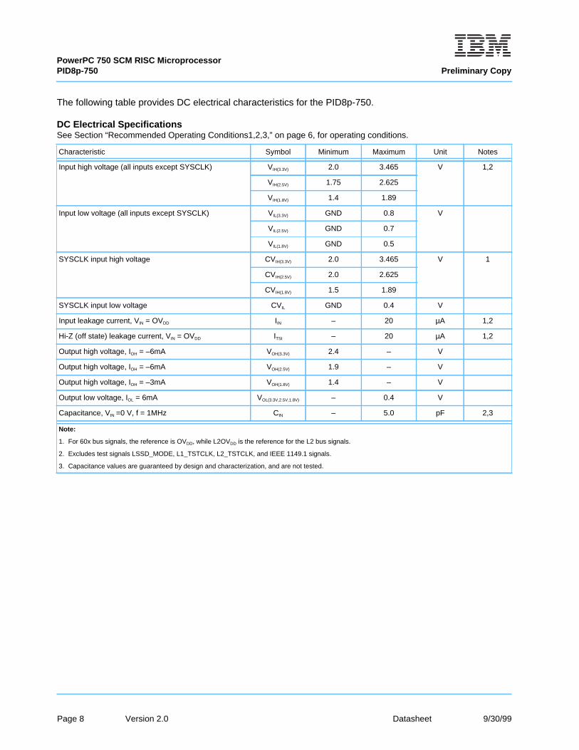
The following table provides DC electrical characteristics for the PID8p-750.
DC Electrical SpecificationsSee Section “Recommended Operating Conditions1,2,3,” on page 6, for operating conditions.
Characteristic Symbol Minimum Maximum Unit Notes
Input high voltage (all inputs except SYSCLK) VIH(3.3V) 2.0 3.465 V 1,2
VIH(2.5V) 1.75 2.625
VIH(1.8V) 1.4 1.89
Input low voltage (all inputs except SYSCLK) VIL(3.3V) GND 0.8 V
VIL(2.5V) GND 0.7
VIL(1.8V) GND 0.5
SYSCLK input high voltage CVIH(3.3V) 2.0 3.465 V 1
CVIH(2.5V) 2.0 2.625
CVIH(1.8V) 1.5 1.89
SYSCLK input low voltage CVIL GND 0.4 V
Input leakage current, VIN = OVDD IIN – 20 µA 1,2
Hi-Z (off state) leakage current, VIN = OVDD ITSI – 20 µA 1,2
Output high voltage, IOH = –6mA VOH(3.3V) 2.4 – V
Output high voltage, IOH = –6mA VOH(2.5V) 1.9 – V
Output high voltage, IOH = –3mA VOH(1.8V) 1.4 – V
Output low voltage, IOL = 6mA VOL(3.3V,2.5V,1.8V) – 0.4 V
Capacitance, VIN =0 V, f = 1MHz CIN – 5.0 pF 2,3
Note:
1. For 60x bus signals, the reference is OVDD, while L2OVDD is the reference for the L2 bus signals.
2. Excludes test signals LSSD_MODE, L1_TSTCLK, L2_TSTCLK, and IEEE 1149.1 signals.
3. Capacitance values are guaranteed by design and characterization, and are not tested.
Page 8 Version 2.0 Datasheet 9/30/99
PowerPC 750 SCM RISC MicroprocessorPreliminary Copy PID8p-750
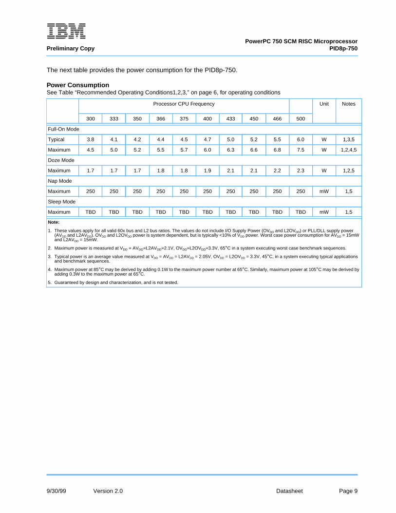
The next table provides the power consumption for the PID8p-750.
Power ConsumptionSee Table “Recommended Operating Conditions1,2,3,” on page 6, for operating conditions
Processor CPU Frequency Unit Notes
300 333 350 366 375 400 433 450 466 500
Full-On Mode
Typical 3.8 4.1 4.2 4.4 4.5 4.7 5.0 5.2 5.5 6.0 W 1,3,5
Maximum 4.5 5.0 5.2 5.5 5.7 6.0 6.3 6.6 6.8 7.5 W 1,2,4,5
Doze Mode
Maximum 1.7 1.7 1.7 1.8 1.8 1.9 2.1 2.1 2.2 2.3 W 1,2,5
Nap Mode
Maximum 250 250 250 250 250 250 250 250 250 250 mW 1,5
Sleep Mode
Maximum TBD TBD TBD TBD TBD TBD TBD TBD TBD TBD mW 1,5
Note:
1. These values apply for all valid 60x bus and L2 bus ratios. The values do not include I/O Supply Power (OVDD and L2OVDD) or PLL/DLL supply power(AVDD and L2AVDD). OVDD and L2OVDD power is system dependent, but is typically <10% of VDD power. Worst case power consumption for AVDD = 15mWand L2AVDD = 15mW.
2. Maximum power is measured at VDD = AVDD=L2AVDD=2.1V, OVDD=L2OVDD=3.3V, 65°C in a system executing worst case benchmark sequences.
3. Typical power is an average value measured at VDD = AVDD = L2AVDD = 2.05V, OVDD = L2OVDD = 3.3V, 45°C, in a system executing typical applicationsand benchmark sequences.
4. Maximum power at 85°C may be derived by adding 0.1W to the maximum power number at 65°C. Similarly, maximum power at 105°C may be derived byadding 0.3W to the maximum power at 65°C.
5. Guaranteed by design and characterization, and is not tested.
9/30/99 Version 2.0 Datasheet Page 9
PowerPC 750 SCM RISC MicroprocessorPID8p-750 Preliminary Copy
AC Electrical Characteristics
This section provides the AC electrical characteristics for the PID8p-750. After fabrication, parts are sorted bymaximum processor core frequency as shown in the Section “Clock AC Specifications,” on page 10, andtested for conformance to the AC specifications for that frequency. These specifications are for 300MHzthrough 400MHz processor core frequencies. The processor core frequency is determined by the bus(SYSCLK) frequency and the settings of the PLL_CFG(0-3) signals. Parts are sold by maximum processorcore frequency; see Section “Ordering Information,” on page 40.
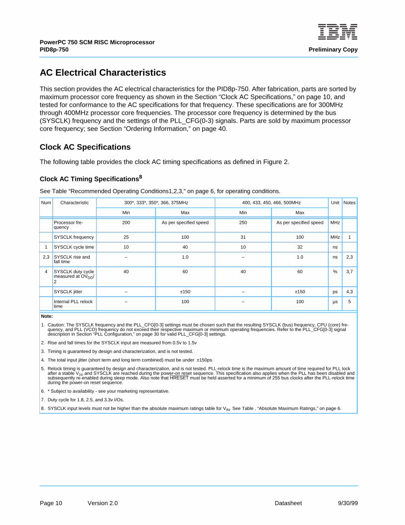
Clock AC Specifications
The following table provides the clock AC timing specifications as defined in Figure 2.
Clock AC Timing Specifications 8
See Table “Recommended Operating Conditions1,2,3,” on page 6, for operating conditions.
Num Characteristic 300*, 333*, 350*, 366, 375MHz 400, 433, 450, 466, 500MHz Unit Notes
Min Max Min Max
Processor fre-quency
200 As per specified speed 250 As per specified speed MHz
SYSCLK frequency 25 100 31 100 MHz 1
1 SYSCLK cycle time 10 40 10 32 ns
2,3 SYSCLK rise andfall time
– 1.0 – 1.0 ns 2,3
4 SYSCLK duty cyclemeasured at OVDD/2
40 60 40 60 % 3,7
SYSCLK jitter – ±150 – ±150 ps 4,3
Internal PLL relocktime
– 100 – 100 µs 5
Note:
1. Caution: The SYSCLK frequency and the PLL_CFG[0-3] settings must be chosen such that the resulting SYSCLK (bus) frequency, CPU (core) fre-quency, and PLL (VCO) frequency do not exceed their respective maximum or minimum operating frequencies. Refer to the PLL_CFG[0-3] signaldescription in Section “PLL Configuration,” on page 30 for valid PLL_CFG[0-3] settings.
2. Rise and fall times for the SYSCLK input are measured from 0.5v to 1.5v
3. Timing is guaranteed by design and characterization, and is not tested.
4. The total input jitter (short term and long term combined) must be under ±150ps.
5. Relock timing is guaranteed by design and characterization, and is not tested. PLL-relock time is the maximum amount of time required for PLL lockafter a stable VDD and SYSCLK are reached during the power-on reset sequence. This specification also applies when the PLL has been disabled andsubsequently re-enabled during sleep mode. Also note that HRESET must be held asserted for a minimum of 255 bus clocks after the PLL-relock timeduring the power-on reset sequence.
6. * Subject to availability - see your marketing representative.
7. Duty cycle for 1.8, 2.5, and 3.3v I/Os.
8. SYSCLK input levels must not be higher than the absolute maximum ratings table for VIN. See Table , “Absolute Maximum Ratings,” on page 6.
Page 10 Version 2.0 Datasheet 9/30/99
PowerPC 750 SCM RISC MicroprocessorPreliminary Copy PID8p-750
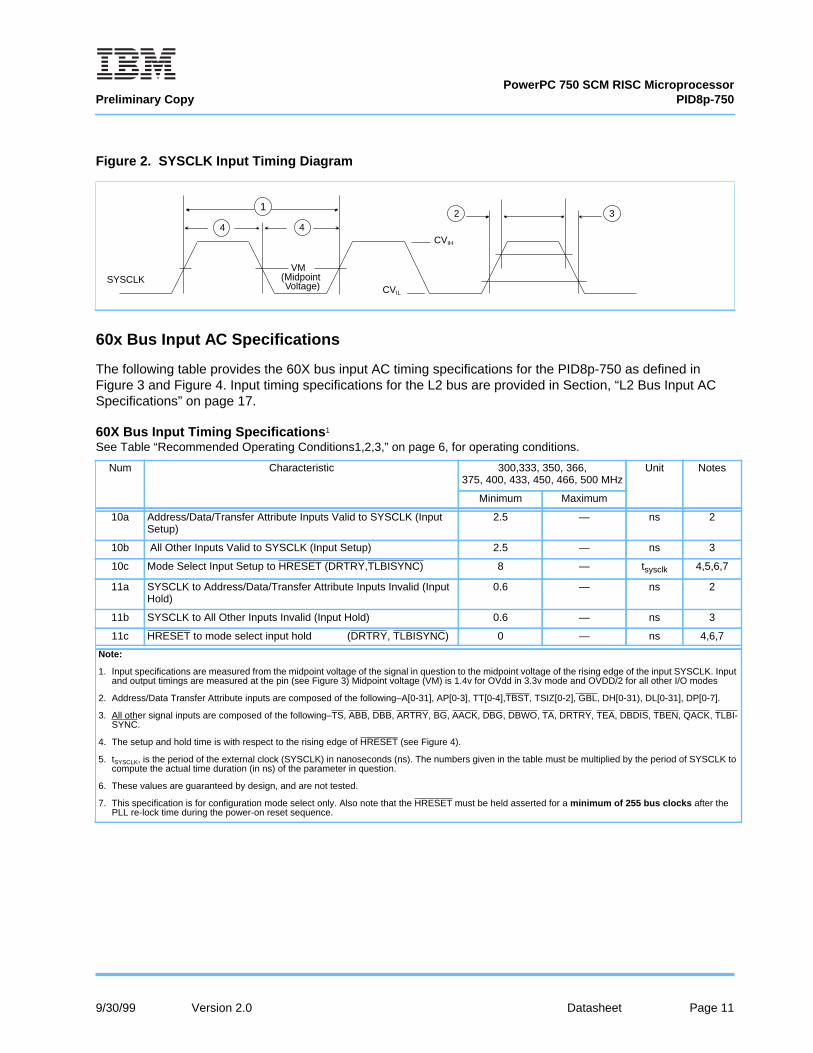
60x Bus Input AC Specifications
The following table provides the 60X bus input AC timing specifications for the PID8p-750 as defined inFigure 3 and Figure 4. Input timing specifications for the L2 bus are provided in Section, “L2 Bus Input ACSpecifications” on page 17.
Figure 2. SYSCLK Input Timing Diagram
60X Bus Input Timing Specifications 1
See Table “Recommended Operating Conditions1,2,3,” on page 6, for operating conditions.
Num Characteristic 300,333, 350, 366,375, 400, 433, 450, 466, 500 MHz
Unit Notes
Minimum Maximum
10a Address/Data/Transfer Attribute Inputs Valid to SYSCLK (InputSetup)
2.5 — ns 2
10b All Other Inputs Valid to SYSCLK (Input Setup) 2.5 — ns 3
10c Mode Select Input Setup to HRESET (DRTRY,TLBISYNC) 8 — tsysclk 4,5,6,7
11a SYSCLK to Address/Data/Transfer Attribute Inputs Invalid (InputHold)
0.6 — ns 2
11b SYSCLK to All Other Inputs Invalid (Input Hold) 0.6 — ns 3
11c HRESET to mode select input hold (DRTRY, TLBISYNC) 0 — ns 4,6,7
Note:
1. Input specifications are measured from the midpoint voltage of the signal in question to the midpoint voltage of the rising edge of the input SYSCLK. Inputand output timings are measured at the pin (see Figure 3) Midpoint voltage (VM) is 1.4v for OVdd in 3.3v mode and OVDD/2 for all other I/O modes
2. Address/Data Transfer Attribute inputs are composed of the following–A[0-31], AP[0-3], TT[0-4],TBST, TSIZ[0-2], GBL, DH[0-31), DL[0-31], DP[0-7].
3. All other signal inputs are composed of the following–TS, ABB, DBB, ARTRY, BG, AACK, DBG, DBWO, TA, DRTRY, TEA, DBDIS, TBEN, QACK, TLBI-SYNC.
4. The setup and hold time is with respect to the rising edge of HRESET (see Figure 4).
5. tSYSCLK, is the period of the external clock (SYSCLK) in nanoseconds (ns). The numbers given in the table must be multiplied by the period of SYSCLK tocompute the actual time duration (in ns) of the parameter in question.
6. These values are guaranteed by design, and are not tested.
7. This specification is for configuration mode select only. Also note that the HRESET must be held asserted for a minimum of 255 bus clocks after thePLL re-lock time during the power-on reset sequence.
VM
CVIL
CVIH
12
4
34
SYSCLK (MidpointVoltage)
9/30/99 Version 2.0 Datasheet Page 11
PowerPC 750 SCM RISC MicroprocessorPID8p-750 Preliminary Copy
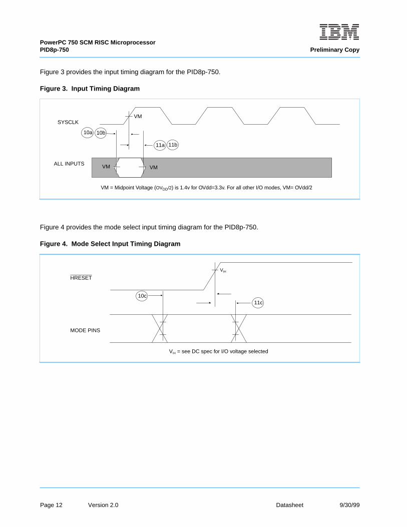
Figure 3 provides the input timing diagram for the PID8p-750.
Figure 4 provides the mode select input timing diagram for the PID8p-750.
Figure 3. Input Timing Diagram
Figure 4. Mode Select Input Timing Diagram
VMSYSCLK
ALL INPUTS
VM = Midpoint Voltage (OVDD/2) is 1.4v for OVdd=3.3v. For all other I/O modes, VM= OVdd/2
10b10a
11b11a
VMVM
VIH
VIH = see DC spec for I/O voltage selected
MODE PINS
10c11c
HRESET
Page 12 Version 2.0 Datasheet 9/30/99
PowerPC 750 SCM RISC MicroprocessorPreliminary Copy PID8p-750
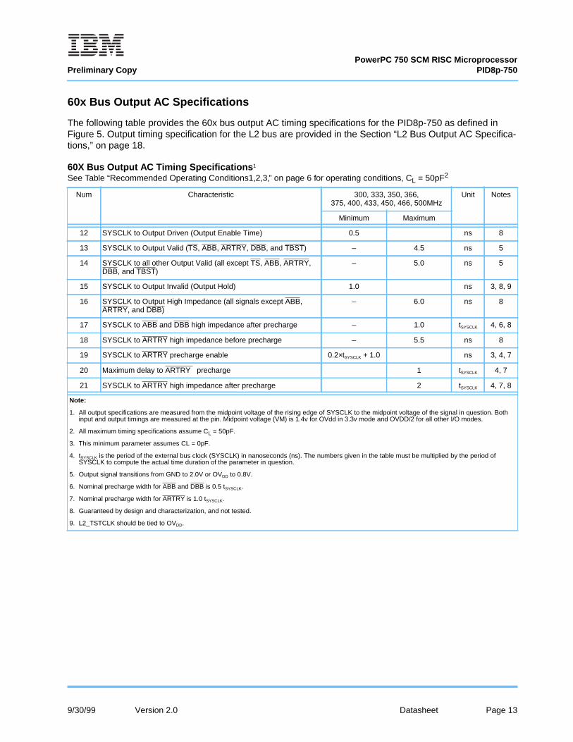
60x Bus Output AC Specifications
The following table provides the 60x bus output AC timing specifications for the PID8p-750 as defined inFigure 5. Output timing specification for the L2 bus are provided in the Section “L2 Bus Output AC Specifica-tions,” on page 18.
60X Bus Output AC Timing Specifications 1
See Table “Recommended Operating Conditions1,2,3,” on page 6 for operating conditions, CL = 50pF2
Num Characteristic 300, 333, 350, 366,375, 400, 433, 450, 466, 500MHz
Unit Notes
Minimum Maximum
12 SYSCLK to Output Driven (Output Enable Time) 0.5 ns 8
13 SYSCLK to Output Valid (TS, ABB, ARTRY, DBB, and TBST) – 4.5 ns 5
14 SYSCLK to all other Output Valid (all except TS, ABB, ARTRY,DBB, and TBST)
– 5.0 ns 5
15 SYSCLK to Output Invalid (Output Hold) 1.0 ns 3, 8, 9
16 SYSCLK to Output High Impedance (all signals except ABB,ARTRY, and DBB)
– 6.0 ns 8
17 SYSCLK to ABB and DBB high impedance after precharge – 1.0 tSYSCLK 4, 6, 8
18 SYSCLK to ARTRY high impedance before precharge – 5.5 ns 8
19 SYSCLK to ARTRY precharge enable 0.2×tSYSCLK + 1.0 ns 3, 4, 7
20 Maximum delay to ARTRY precharge 1 tSYSCLK 4, 7
21 SYSCLK to ARTRY high impedance after precharge 2 tSYSCLK 4, 7, 8
Note:
1. All output specifications are measured from the midpoint voltage of the rising edge of SYSCLK to the midpoint voltage of the signal in question. Bothinput and output timings are measured at the pin. Midpoint voltage (VM) is 1.4v for OVdd in 3.3v mode and OVDD/2 for all other I/O modes.
2. All maximum timing specifications assume CL = 50pF.
3. This minimum parameter assumes CL = 0pF.
4. tSYSCLK is the period of the external bus clock (SYSCLK) in nanoseconds (ns). The numbers given in the table must be multiplied by the period ofSYSCLK to compute the actual time duration of the parameter in question.
5. Output signal transitions from GND to 2.0V or OVDD to 0.8V.
6. Nominal precharge width for ABB and DBB is 0.5 tSYSCLK.
7. Nominal precharge width for ARTRY is 1.0 tSYSCLK.
8. Guaranteed by design and characterization, and not tested.
9. L2_TSTCLK should be tied to OVDD.
9/30/99 Version 2.0 Datasheet Page 13
PowerPC 750 SCM RISC MicroprocessorPID8p-750 Preliminary Copy
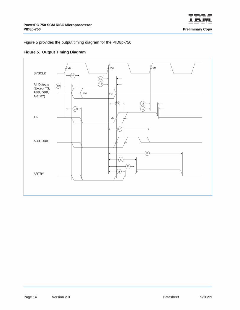
Figure 5 provides the output timing diagram for the PID8p-750.
Figure 5. Output Timing Diagram
SYSCLK
All Outputs(Except TS,ABB, DBB,ARTRY)
TS
ABB, DBB
ARTRY
12
14
13
15
16
16
VM VM
15
VM
13
20
18
17
21
19
VM VM
VM
Page 14 Version 2.0 Datasheet 9/30/99
PowerPC 750 SCM RISC MicroprocessorPreliminary Copy PID8p-750
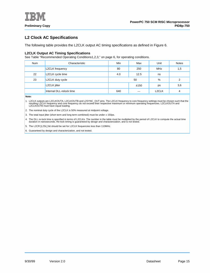
L2 Clock AC Specifications
The following table provides the L2CLK output AC timing specifications as defined in Figure 6.
L2CLK Output AC Timing SpecificationsSee Table “Recommended Operating Conditions1,2,3,” on page 6, for operating conditions.
Num Characteristic Min Max Unit Notes
L2CLK frequency 80 250 MHz 1,5
22 L2CLK cycle time 4.0 12.5 ns
23 L2CLK duty cycle 50 % 2
L2CLK jitter ±150 ps 3,6
Internal DLL-relock time 640 — L2CLK 4
Note:
1. L2CLK outputs are L2CLKOUTA, L2CLKOUTB and L2SYNC_OUT pins. The L2CLK frequency to core frequency settings must be chosen such that theresulting L2CLK frequency and core frequency do not exceed their respective maximum or minimum operating frequencies. L2CLKOUTA andL2CLKOUTB must have equal loading.
2. The nominal duty cycle of the L2CLK is 50% measured at midpoint voltage.
3. The total input jitter (short term and long term combined) must be under ± 150ps.
4. The DLL re-lock time is specified in terms of L2CLKs. The number in the table must be multiplied by the period of L2CLK to compute the actual timeduration in nanoseconds. Re-lock timing is guaranteed by design and characterization, and is not tested.
5. The L2CR [L2SL] bit should be set for L2CLK frequencies less than 110MHz.
6. Guaranteed by design and characterization, and not tested.
9/30/99 Version 2.0 Datasheet Page 15
PowerPC 750 SCM RISC MicroprocessorPID8p-750 Preliminary Copy
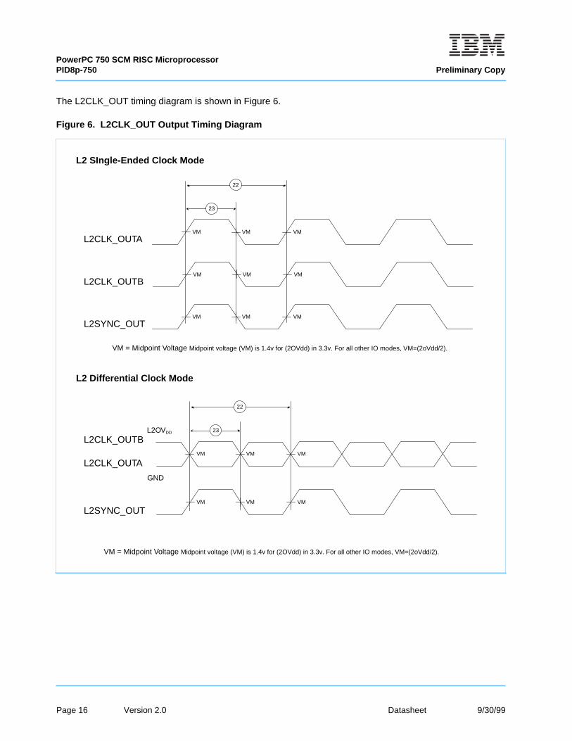
The L2CLK_OUT timing diagram is shown in Figure 6.
Figure 6. L2CLK_OUT Output Timing Diagram
VM
VM = Midpoint Voltage Midpoint voltage (VM) is 1.4v for (2OVdd) in 3.3v. For all other IO modes, VM=(2oVdd/2).
22
L2CLK_OUTAVM VM
23
VM
VM = Midpoint Voltage Midpoint voltage (VM) is 1.4v for (2OVdd) in 3.3v. For all other IO modes, VM=(2oVdd/2).
22
L2CLK_OUTAVM VM
23
L2CLK_OUTB
GND
L2OVDD
VM
L2CLK_OUTBVM VM
VM
L2SYNC_OUTVM VM
VM
L2SYNC_OUTVM VM
L2 SIngle-Ended Clock Mode
L2 Differential Clock Mode
Page 16 Version 2.0 Datasheet 9/30/99
PowerPC 750 SCM RISC MicroprocessorPreliminary Copy PID8p-750
L2 Bus Input AC Specifications
The L2 bus input interface AC timing specifications are found in the following table.
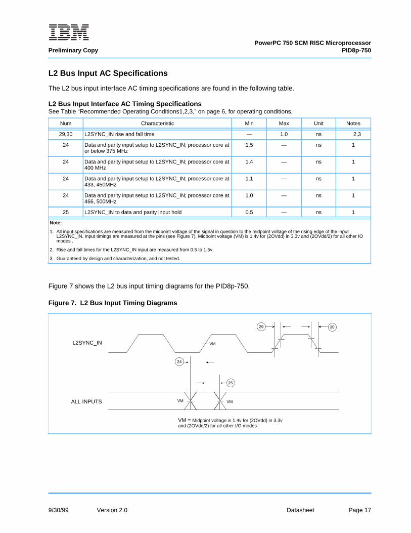
Figure 7 shows the L2 bus input timing diagrams for the PID8p-750.
L2 Bus Input Interface AC Timing SpecificationsSee Table “Recommended Operating Conditions1,2,3,” on page 6, for operating conditions.
Num Characteristic Min Max Unit Notes
29,30 L2SYNC_IN rise and fall time — 1.0 ns 2,3
24 Data and parity input setup to L2SYNC_IN; processor core ator below 375 MHz
1.5 — ns 1
24 Data and parity input setup to L2SYNC_IN; processor core at400 MHz
1.4 — ns 1
24 Data and parity input setup to L2SYNC_IN; processor core at433, 450MHz
1.1 — ns 1
24 Data and parity input setup to L2SYNC_IN; processor core at466, 500MHz
1.0 — ns 1
25 L2SYNC_IN to data and parity input hold 0.5 — ns 1
Note:
1. All input specifications are measured from the midpoint voltage of the signal in question to the midpoint voltage of the rising edge of the inputL2SYNC_IN. Input timings are measured at the pins (see Figure 7). Midpoint voltage (VM) is 1.4v for (2OVdd) in 3.3v and (2OVdd/2) for all other IOmodes .
2. Rise and fall times for the L2SYNC_IN input are measured from 0.5 to 1.5v.
3. Guaranteed by design and characterization, and not tested.
Figure 7. L2 Bus Input Timing Diagrams
VM
VM = Midpoint voltage is 1.4v for (2OVdd) in 3.3v
L2SYNC_IN
25
24
ALL INPUTS
29 30
VMVM
and (2OVdd/2) for all other I/O modes
9/30/99 Version 2.0 Datasheet Page 17
PowerPC 750 SCM RISC MicroprocessorPID8p-750 Preliminary Copy
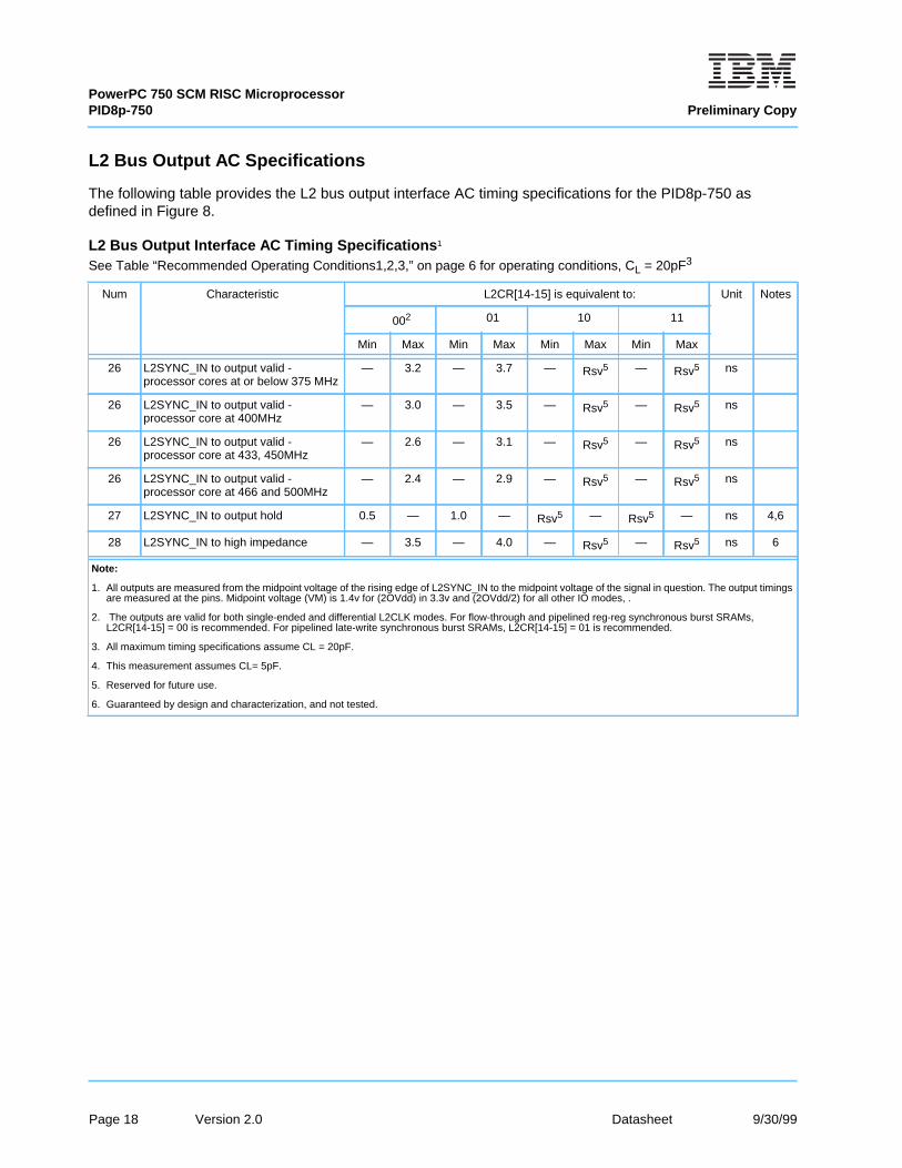
L2 Bus Output AC Specifications
The following table provides the L2 bus output interface AC timing specifications for the PID8p-750 asdefined in Figure 8.
L2 Bus Output Interface AC Timing Specifications 1
See Table “Recommended Operating Conditions1,2,3,” on page 6 for operating conditions, CL = 20pF3
Num Characteristic L2CR[14-15] is equivalent to: Unit Notes
002 01 10 11
Min Max Min Max Min Max Min Max
26 L2SYNC_IN to output valid -processor cores at or below 375 MHz
— 3.2 — 3.7 — Rsv5 — Rsv5 ns
26 L2SYNC_IN to output valid -processor core at 400MHz
— 3.0 — 3.5 — Rsv5 — Rsv5 ns
26 L2SYNC_IN to output valid -processor core at 433, 450MHz
— 2.6 — 3.1 — Rsv5 — Rsv5 ns
26 L2SYNC_IN to output valid -processor core at 466 and 500MHz
— 2.4 — 2.9 — Rsv5 — Rsv5 ns
27 L2SYNC_IN to output hold 0.5 — 1.0 — Rsv5 — Rsv5 — ns 4,6
28 L2SYNC_IN to high impedance — 3.5 — 4.0 — Rsv5 — Rsv5 ns 6
Note:
1. All outputs are measured from the midpoint voltage of the rising edge of L2SYNC_IN to the midpoint voltage of the signal in question. The output timingsare measured at the pins. Midpoint voltage (VM) is 1.4v for (2OVdd) in 3.3v and (2OVdd/2) for all other IO modes, .
2. The outputs are valid for both single-ended and differential L2CLK modes. For flow-through and pipelined reg-reg synchronous burst SRAMs,L2CR[14-15] = 00 is recommended. For pipelined late-write synchronous burst SRAMs, L2CR[14-15] = 01 is recommended.
3. All maximum timing specifications assume CL = 20pF.
4. This measurement assumes CL= 5pF.
5. Reserved for future use.
6. Guaranteed by design and characterization, and not tested.
Page 18 Version 2.0 Datasheet 9/30/99
PowerPC 750 SCM RISC MicroprocessorPreliminary Copy PID8p-750
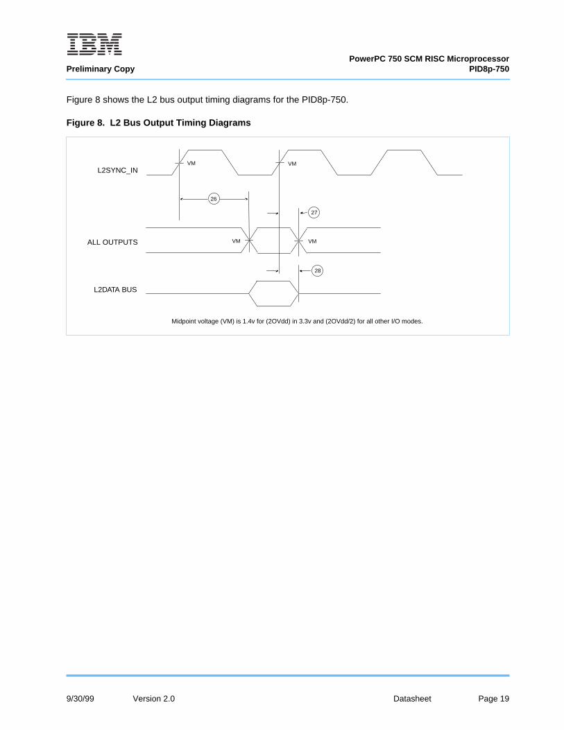
Figure 8 shows the L2 bus output timing diagrams for the PID8p-750.
Figure 8. L2 Bus Output Timing Diagrams
27
VML2SYNC_IN
26
ALL OUTPUTS
VM
28
L2DATA BUS
VMVM
Midpoint voltage (VM) is 1.4v for (2OVdd) in 3.3v and (2OVdd/2) for all other I/O modes.
9/30/99 Version 2.0 Datasheet Page 19
PowerPC 750 SCM RISC MicroprocessorPID8p-750 Preliminary Copy
IEEE 1149.1 AC Timing Specifications
The table below provides the IEEE 1149.1 (JTAG) AC timing specifications as defined in Figure 9, Figure 10,Figure 11, and Figure 12. The five JTAG signals are; TDI, TDO, TMS, TCK, and TRST.
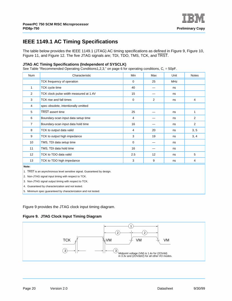
Figure 9 provides the JTAG clock input timing diagram.
JTAG AC Timing Specifications (Independent of SYSCLK)See Table “Recommended Operating Conditions1,2,3,” on page 6 for operating conditions, CL = 50pF.
Num Characteristic Min Max Unit Notes
TCK frequency of operation 0 25 MHz
1 TCK cycle time 40 — ns
2 TCK clock pulse width measured at 1.4V 15 — ns
3 TCK rise and fall times 0 2 ns 4
4 spec obsolete, intentionally omitted
5 TRST assert time 25 — ns 1
6 Boundary-scan input data setup time 4 — ns 2
7 Boundary-scan input data hold time 16 — ns 2
8 TCK to output data valid 4 20 ns 3, 5
9 TCK to output high impedance 3 19 ns 3, 4
10 TMS, TDI data setup time 0 — ns
11 TMS, TDI data hold time 16 — ns
12 TCK to TDO data valid 2.5 12 ns 5
13 TCK to TDO high impedance 3 9 ns 4
Note:
1. TRST is an asynchronous level sensitive signal. Guaranteed by design.
2. Non-JTAG signal input timing with respect to TCK.
3. Non-JTAG signal output timing with respect to TCK.
4. Guaranteed by characterization and not tested.
5. Minimum spec guaranteed by characterization and not tested.
Figure 9. JTAG Clock Input Timing Diagram
1
2 2
3 3
VMTCK VM VM
Midpoint voltage (VM) is 1.4v for (2OVdd)in 3.3v and (2OVdd/2) for all other I/O modes.
Page 20 Version 2.0 Datasheet 9/30/99
PowerPC 750 SCM RISC MicroprocessorPreliminary Copy PID8p-750
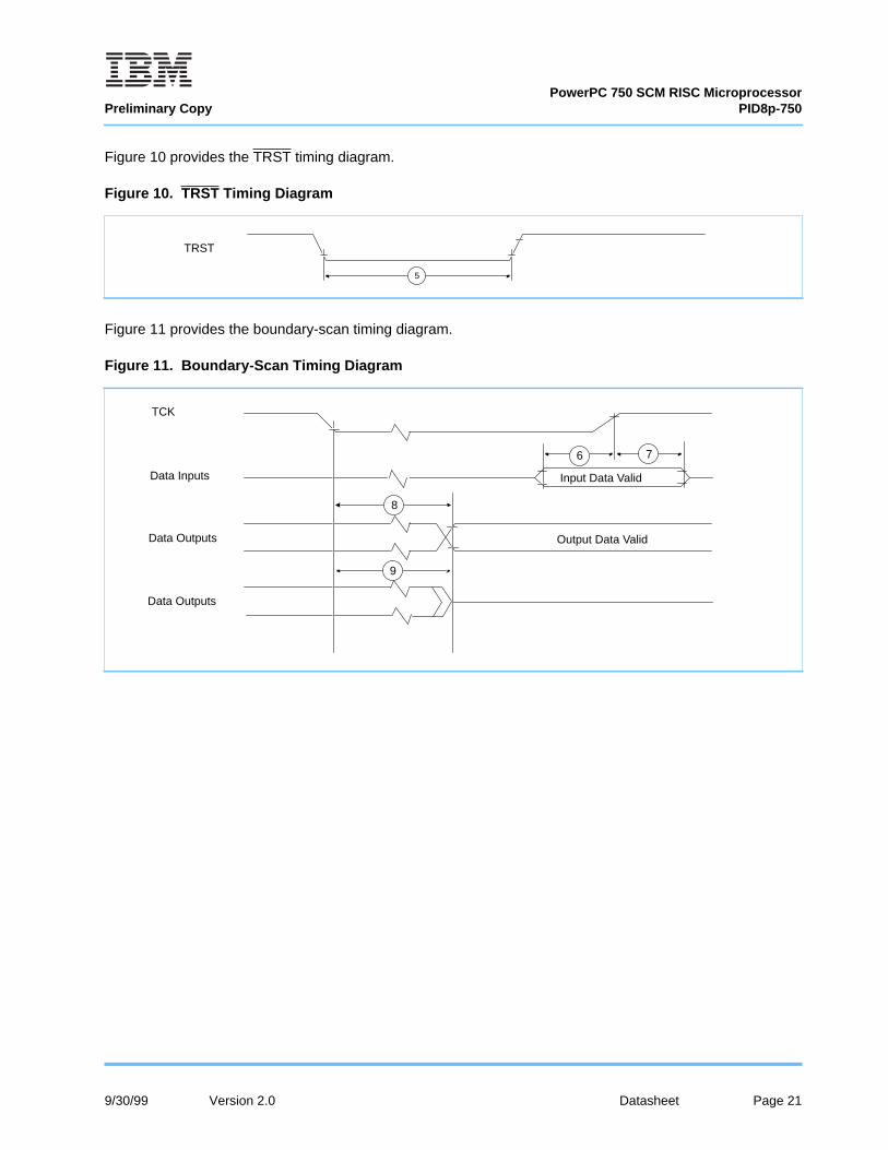
Figure 10 provides the TRST timing diagram.
Figure 11 provides the boundary-scan timing diagram.
Figure 10. TRST Timing Diagram
Figure 11. Boundary-Scan Timing Diagram
5
TRST
9
6 7
8
9
TCK
Data Inputs
Data Outputs
Data Outputs
Input Data Valid
Output Data Valid
9/30/99 Version 2.0 Datasheet Page 21
PowerPC 750 SCM RISC MicroprocessorPID8p-750 Preliminary Copy
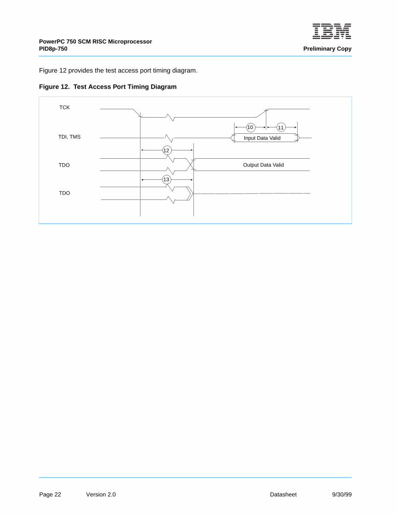
Figure 12 provides the test access port timing diagram.
Figure 12. Test Access Port Timing Diagram
913
12
10 11
TCK
TDI, TMS
TDO
TDO
Input Data Valid
Output Data Valid
Page 22 Version 2.0 Datasheet 9/30/99
PowerPC 750 SCM RISC MicroprocessorPreliminary Copy PID8p-750
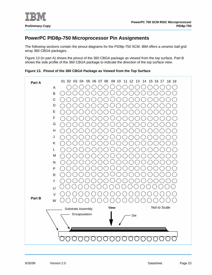
PowerPC PID8p-750 Microprocessor Pin Assignments
The following sections contain the pinout diagrams for the PID8p-750 SCM. IBM offers a ceramic ball gridarray 360 CBGA packages.
Figure 13 (in part A) shows the pinout of the 360 CBGA package as viewed from the top surface. Part Bshows the side profile of the 360 CBGA package to indicate the direction of the top surface view.
Figure 13. Pinout of the 360 CBGA Package as Viewed from the Top Surface
A
B
C
D
E
F
G
H
J
K
L
M
N
P
R
T
01 02 03 04 05 06 07 08 09 10 11 12 13 14 15 16
Not to ScaleSubstrate Assembly.
Encapsulation
View
Part B
Die
Part A 17 18 19
U
V
W
9/30/99 Version 2.0 Datasheet Page 23
PowerPC 750 SCM RISC MicroprocessorPID8p-750 Preliminary Copy
PowerPC PID8p-750 Microprocessor Pinout Listings
The following table provides the pinout listing for the 360 CBGA package (the PID8p-750).
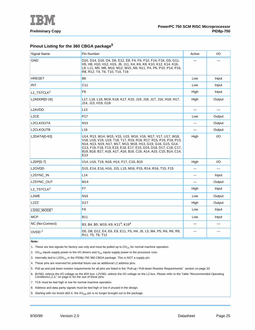
Pinout Listing for the 360 CBGA package 5
Signal Name Pin Number Active I/O
A0-A31 A13, D2, H11, C1, B13, F2, C13, E5, D13, G7, F12, G3, G6, H2, E2,L3, G5, L4, G4, J4, H7, E1, G2, F3, J7, M3, H3, J2, J6, K3, K2, L2
High I/O
AACK N3 Low Input
ABB L7 Low I/O
AP0-AP38 C4, C5, C6, C7 High I/O
ARTRY L6 Low I/O
AVDD 9 A8 — —
BG H1 Low Input
BR E7 Low Output
CKSTP_OUT D7 Low Output
CI C2 Low Output
CKSTP_IN B8 Low Input
CLKOUT E3 -- Output
DBB K5 Low I/O
DBDIS G1 Low Input
DBG K1 Low Input
DBWO D1 Low Input
DH0-DH31 W12, W11, V11, T9, W10, U9, U10, M11, M9, P8, W7, P9, W9, R10,W6, V7, V6, U8, V9, T7, U7, R7, U6, W5, U5, W4, P7, V5, V4, W3,U4, R5
High I/O
DL0-DL31 M6, P3, N4, N5, R3, M7, T2, N6, U2, N7, P11, V13, U12, P12, T13,W13, U13, V10, W8, T11, U11, V12, V8, T1, P1, V1, U1, N1, R2, V3,U3, W2
High I/O
DP0-DP78 L1, P2, M2, V2, M1, N2, T3, R1 High I/O
DRTRY H6 Low Input
GBL B1 Low I/O
Note:
1. These are test signals for factory use only and must be pulled up to OVDD for normal machine operation.
2. OVDD inputs supply power to the I/O drivers and VDD inputs supply power to the processor core.
3. Internally tied to L2OVDD in the PID8p-750 360 CBGA package. This is NOT a supply pin.
4. These pins are reserved for potential future use as additional L2 address pins.
5. Pull up and pull down resistor requirements for all pins are listed in the “Pull-up / Pull-down Resistor Requirements” section on page 33
6. BVSEL selects the I/O voltage on the 60X bus. L2VSEL selects the I/O voltage on the L2 bus. Please refer to the Table “Recommended OperatingConditions1,2,3,” on page 6, for the use of these pins.
7. TCK must be tied high or low for normal machine operation.
8. Address and data parity signals must be tied high or low if unused in the design.
9. Starting with rev levels dd3.X, the AVDD pin is no longer brought out to the package.
Page 24 Version 2.0 Datasheet 9/30/99
PowerPC 750 SCM RISC MicroprocessorPreliminary Copy PID8p-750
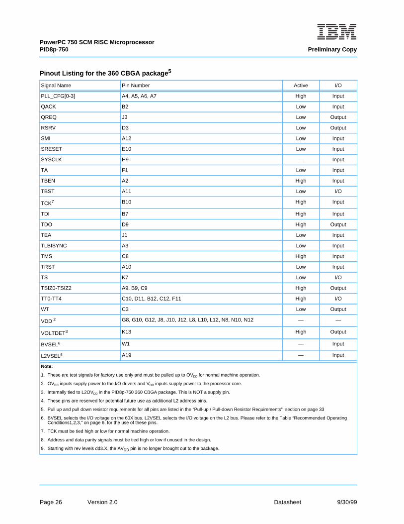
GND D10, D14, D16, D4, D6, E12, E8, F4, F6, F10, F14, F16, G9, G11,H5, H8, H10, H12, H15, J9, J11, K4, K6, K8, K10, K12, K14, K16,L9, L11, M5, M8, M10, M12, M15, N9, N11, P4, P6, P10, P14, P16,R8, R12, T4, T6, T10, T14, T16
— —
HRESET B6 Low Input
INT C11 Low Input
L1_TSTCLK1 F8 High Input
L2ADDR[0-16] L17, L18, L19, M19, K18, K17, K15, J19, J18, J17, J16, H18, H17,J14, J13, H19, G18
High Output
L2AVDD L13 — —
L2CE P17 Low Output
L2CLKOUTA N15 — Output
L2CLKOUTB L16 — Output
L2DATA[0-63] U14, R13, W14, W15, V15, U15, W16, V16, W17, V17, U17, W18,V18, U18, V19, U19, T18, T17, R19, R18, R17, R15, P19, P18, P13,N14, N13, N19, N17, M17, M13, M18, H13, G19, G16, G15, G14,G13, F19, F18, F13, E19, E18, E17, E15, D19, D18, D17, C18, C17,B19, B18, B17, A18, A17, A16, B16, C16, A14, A15, C15, B14, C14,E13
High I/O
L2DP[0-7] V14, U16, T19, N18, H14, F17, C19, B15 High I/O
L2OVDD D15, E14, E16, H16, J15, L15, M16, P15, R14, R16, T15, F15 — —
L2SYNC_IN L14 — Input
L2SYNC_OUT M14 — Output
L2_TSTCLK1 F7 High Input
L2WE N16 Low Output
L2ZZ G17 High Output
LSSD_MODE1 F9 Low Input
MCP B11 Low Input
NC (No-Connect) B3, B4, B5, W19, K9, K114, K194 — —
OVDD 2 D5, D8, D12, E4, E6, E9, E11, F5, H4, J5, L5, M4, P5, R4, R6, R9,R11, T5, T8, T12
— —
Pinout Listing for the 360 CBGA package 5
Signal Name Pin Number Active I/O
Note:
1. These are test signals for factory use only and must be pulled up to OVDD for normal machine operation.
2. OVDD inputs supply power to the I/O drivers and VDD inputs supply power to the processor core.
3. Internally tied to L2OVDD in the PID8p-750 360 CBGA package. This is NOT a supply pin.
4. These pins are reserved for potential future use as additional L2 address pins.
5. Pull up and pull down resistor requirements for all pins are listed in the “Pull-up / Pull-down Resistor Requirements” section on page 33
6. BVSEL selects the I/O voltage on the 60X bus. L2VSEL selects the I/O voltage on the L2 bus. Please refer to the Table “Recommended OperatingConditions1,2,3,” on page 6, for the use of these pins.
7. TCK must be tied high or low for normal machine operation.
8. Address and data parity signals must be tied high or low if unused in the design.
9. Starting with rev levels dd3.X, the AVDD pin is no longer brought out to the package.
9/30/99 Version 2.0 Datasheet Page 25
PowerPC 750 SCM RISC MicroprocessorPID8p-750 Preliminary Copy
PLL_CFG[0-3] A4, A5, A6, A7 High Input
QACK B2 Low Input
QREQ J3 Low Output
RSRV D3 Low Output
SMI A12 Low Input
SRESET E10 Low Input
SYSCLK H9 — Input
TA F1 Low Input
TBEN A2 High Input
TBST A11 Low I/O
TCK7 B10 High Input
TDI B7 High Input
TDO D9 High Output
TEA J1 Low Input
TLBISYNC A3 Low Input
TMS C8 High Input
TRST A10 Low Input
TS K7 Low I/O
TSIZ0-TSIZ2 A9, B9, C9 High Output
TT0-TT4 C10, D11, B12, C12, F11 High I/O
WT C3 Low Output
VDD 2 G8, G10, G12, J8, J10, J12, L8, L10, L12, N8, N10, N12 — —
VOLTDET3 K13 High Output
BVSEL6 W1 — Input
L2VSEL6 A19 — Input
Pinout Listing for the 360 CBGA package 5
Signal Name Pin Number Active I/O
Note:
1. These are test signals for factory use only and must be pulled up to OVDD for normal machine operation.
2. OVDD inputs supply power to the I/O drivers and VDD inputs supply power to the processor core.
3. Internally tied to L2OVDD in the PID8p-750 360 CBGA package. This is NOT a supply pin.
4. These pins are reserved for potential future use as additional L2 address pins.
5. Pull up and pull down resistor requirements for all pins are listed in the “Pull-up / Pull-down Resistor Requirements” section on page 33
6. BVSEL selects the I/O voltage on the 60X bus. L2VSEL selects the I/O voltage on the L2 bus. Please refer to the Table “Recommended OperatingConditions1,2,3,” on page 6, for the use of these pins.
7. TCK must be tied high or low for normal machine operation.
8. Address and data parity signals must be tied high or low if unused in the design.
9. Starting with rev levels dd3.X, the AVDD pin is no longer brought out to the package.
Page 26 Version 2.0 Datasheet 9/30/99
PowerPC 750 SCM RISC MicroprocessorPreliminary Copy PID8p-750
PowerPC PID8p-750 Microprocessor Package Description
The following sections provide the package parameters and the mechanical dimensions for the PID8p-750.
Parameters for the 360 CBGA Package
The package parameters are as provided in the following list. The package type is 25 x 25mm, 360-leadceramic ball grid array (CBGA).
Package outline 25 x 25mm
Interconnects 360 (19 x 19 ball array - 1)
Pitch 1.27mm (50mil)
Minimum module height 2.65mm
Maximum module height 3.20mm
Ball diameter 0.89mm (35mil)
9/30/99 Version 2.0 Datasheet Page 27
PowerPC 750 SCM RISC MicroprocessorPID8p-750 Preliminary Copy
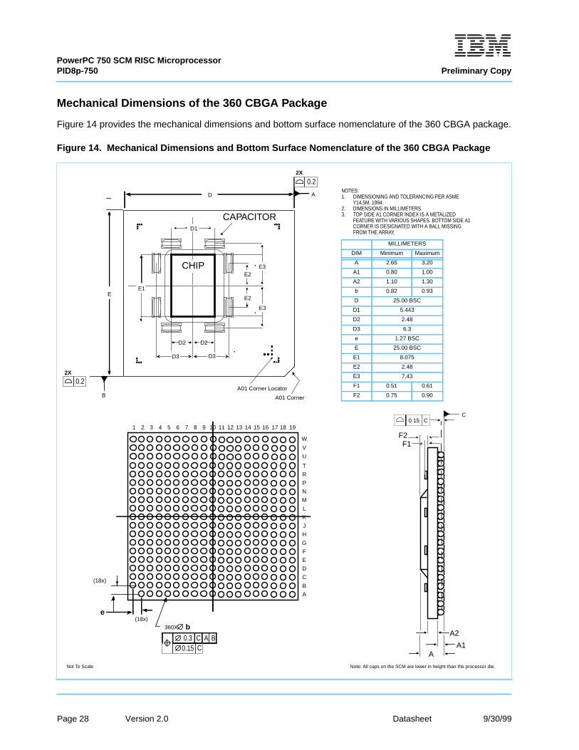
Mechanical Dimensions of the 360 CBGA Package
Figure 14 provides the mechanical dimensions and bottom surface nomenclature of the 360 CBGA package.
Figure 14. Mechanical Dimensions and Bottom Surface Nomenclature of the 360 CBGA Package
NOTES:1. DIMENSIONING AND TOLERANCING PER ASME
Y14.5M, 1994.2. DIMENSIONS IN MILLIMETERS.3. TOP SIDE A1 CORNER INDEX IS A METALIZED
FEATURE WITH VARIOUS SHAPES. BOTTOM SIDE A1CORNER IS DESIGNATED WITH A BALL MISSINGFROM THE ARRAY.
MILLIMETERS
DIM Minimum Maximum
A 2.65 3.20
A1 0.80 1.00
A2 1.10 1.30
b 0.82 0.93
D 25.00 BSC
D1 5.443
D2 2.48
D3 6.3
e 1.27 BSC
E 25.00 BSC
E1 8.075
E2 2.48
E3 7.43
F1 0.51 0.61
F2 0.75 0.90
e
1 2 3 4 5 6 7 8 9 10 11 12 13 14 15 16 17 18 19
U
V
W
A
B
C
D
E
F
G
H
J
K
L
M
N
P
R
T
BC
360X
A0.3C0.15
b
AA1
A2
C0.15 C
Not To Scale
(18x)
(18x)
0.2
D
2X
EE1
D1
0.22X
B
A
A01 Corner Locator
A01 Corner
CHIP
D2
D3
D2
D3
E3E2
E3
E2
CAPACITOR
Note: All caps on the SCM are lower in height than the processor die.
F2F1
Page 28 Version 2.0 Datasheet 9/30/99
PowerPC 750 SCM RISC MicroprocessorPreliminary Copy PID8p-750
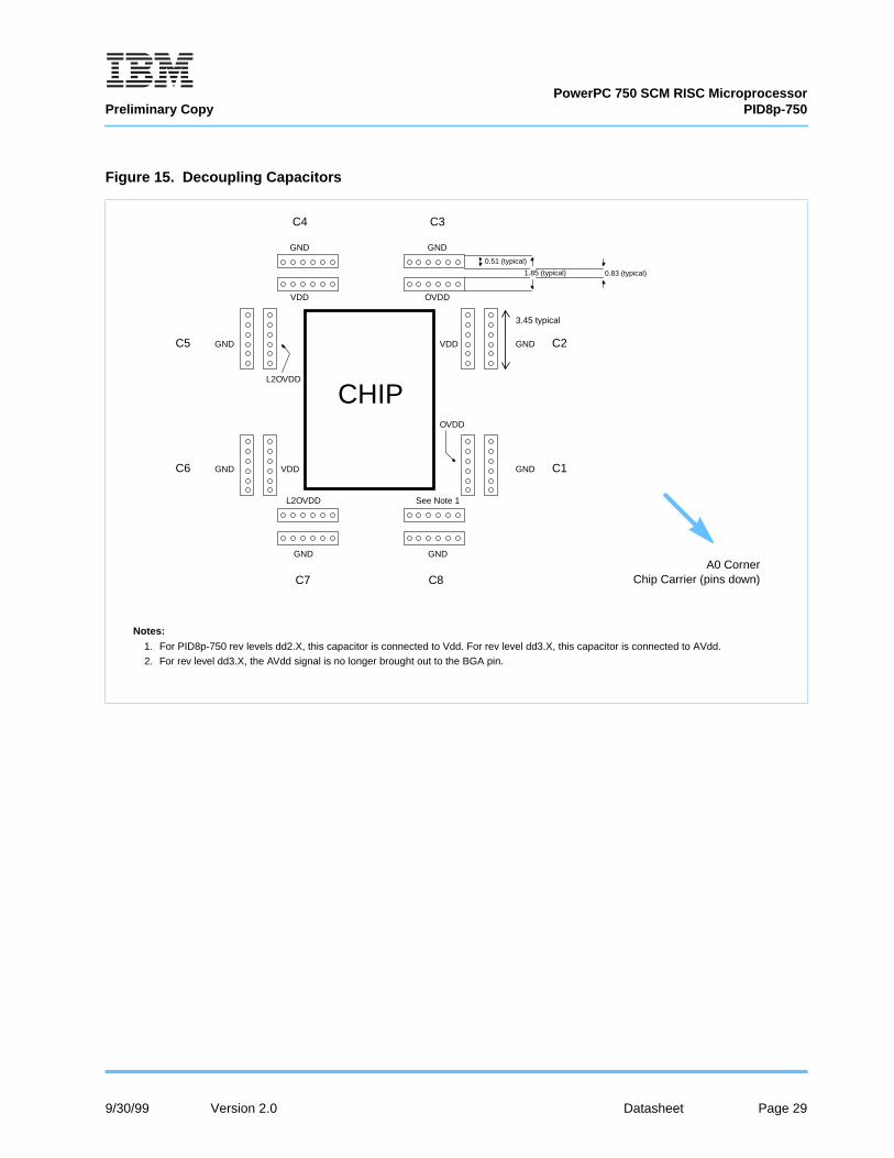
Figure 15. Decoupling Capacitors
L2OVDD
L2OVDD
VDDGND
GND
GNDGND
GND
GND
OVDD
See Note 1
VDD
VDD OVDD
GND GND
C1
C2
C3C4
C5
C6
C7 C8A0 Corner
Chip Carrier (pins down)
CHIP
0.83 (typical)1.85 (typical)
0.51 (typical)
3.45 typical
Notes:
1. For PID8p-750 rev levels dd2.X, this capacitor is connected to Vdd. For rev level dd3.X, this capacitor is connected to AVdd.
2. For rev level dd3.X, the AVdd signal is no longer brought out to the BGA pin.
9/30/99 Version 2.0 Datasheet Page 29
PowerPC 750 SCM RISC MicroprocessorPID8p-750 Preliminary Copy
System Design Information
This section provides electrical and thermal design recommendations for successful application of the PID8p-750.
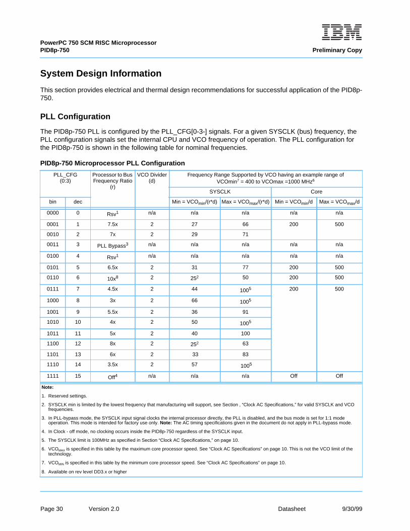
PLL Configuration
The PID8p-750 PLL is configured by the PLL_CFG[0-3-] signals. For a given SYSCLK (bus) frequency, thePLL configuration signals set the internal CPU and VCO frequency of operation. The PLL configuration forthe PID8p-750 is shown in the following table for nominal frequencies.
PID8p-750 Microprocessor PLL Configuration
PLL_CFG(0:3)
Processor to BusFrequency Ratio
(r)
VCO Divider(d)
Frequency Range Supported by VCO having an example range ofVCOmin7 = 400 to VCOmax =1000 MHz6
SYSCLK Core
bin dec Min = VCOmin/(r*d) Max = VCOmax/(r*d) Min = VCOmin/d Max = VCOmax/d
0000 0 Rsv1 n/a n/a n/a n/a n/a
0001 1 7.5x 2 27 66 200 500
0010 2 7x 2 29 71
0011 3 PLL Bypass3 n/a n/a n/a n/a n/a
0100 4 Rsv1 n/a n/a n/a n/a n/a
0101 5 6.5x 2 31 77 200 500
0110 6 10x8 2 252 50 200 500
0111 7 4.5x 2 44 1005 200 500
1000 8 3x 2 66 1005
1001 9 5.5x 2 36 91
1010 10 4x 2 50 1005
1011 11 5x 2 40 100
1100 12 8x 2 252 63
1101 13 6x 2 33 83
1110 14 3.5x 2 57 1005
1111 15 Off4 n/a n/a n/a Off Off
Note:
1. Reserved settings.
2. SYSCLK min is limited by the lowest frequency that manufacturing will support, see Section , “Clock AC Specifications,” for valid SYSCLK and VCOfrequencies.
3. In PLL-bypass mode, the SYSCLK input signal clocks the internal processor directly, the PLL is disabled, and the bus mode is set for 1:1 modeoperation. This mode is intended for factory use only. Note: The AC timing specifications given in the document do not apply in PLL-bypass mode.
4. In Clock - off mode, no clocking occurs inside the PID8p-750 regardless of the SYSCLK input.
5. The SYSCLK limit is 100MHz as specified in Section “Clock AC Specifications,” on page 10.
6. VCOMAX is specified in this table by the maximum core processor speed. See “Clock AC Specifications” on page 10. This is not the VCO limit of thetechnology.
7. VCOMIN is specified in this table by the minimum core processor speed. See “Clock AC Specifications” on page 10.
8. Available on rev level DD3.x or higher
Page 30 Version 2.0 Datasheet 9/30/99
PowerPC 750 SCM RISC MicroprocessorPreliminary Copy PID8p-750
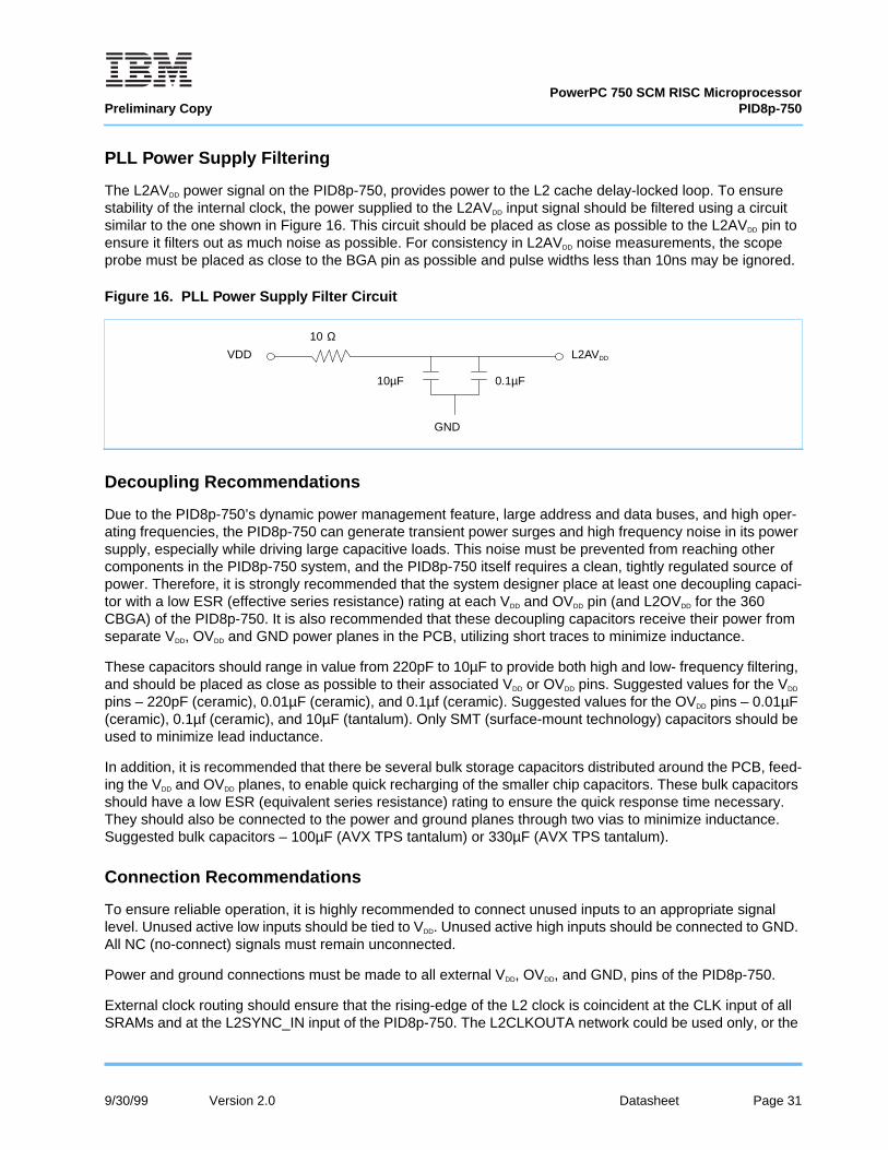
PLL Power Supply Filtering
The L2AVDD power signal on the PID8p-750, provides power to the L2 cache delay-locked loop. To ensurestability of the internal clock, the power supplied to the L2AVDD input signal should be filtered using a circuitsimilar to the one shown in Figure 16. This circuit should be placed as close as possible to the L2AVDD pin toensure it filters out as much noise as possible. For consistency in L2AVDD noise measurements, the scopeprobe must be placed as close to the BGA pin as possible and pulse widths less than 10ns may be ignored.
Decoupling Recommendations
Due to the PID8p-750’s dynamic power management feature, large address and data buses, and high oper-ating frequencies, the PID8p-750 can generate transient power surges and high frequency noise in its powersupply, especially while driving large capacitive loads. This noise must be prevented from reaching othercomponents in the PID8p-750 system, and the PID8p-750 itself requires a clean, tightly regulated source ofpower. Therefore, it is strongly recommended that the system designer place at least one decoupling capaci-tor with a low ESR (effective series resistance) rating at each VDD and OVDD pin (and L2OVDD for the 360CBGA) of the PID8p-750. It is also recommended that these decoupling capacitors receive their power fromseparate VDD, OVDD and GND power planes in the PCB, utilizing short traces to minimize inductance.
These capacitors should range in value from 220pF to 10µF to provide both high and low- frequency filtering,and should be placed as close as possible to their associated VDD or OVDD pins. Suggested values for the VDD
pins – 220pF (ceramic), 0.01µF (ceramic), and 0.1µf (ceramic). Suggested values for the OVDD pins – 0.01µF(ceramic), 0.1µf (ceramic), and 10µF (tantalum). Only SMT (surface-mount technology) capacitors should beused to minimize lead inductance.
In addition, it is recommended that there be several bulk storage capacitors distributed around the PCB, feed-ing the VDD and OVDD planes, to enable quick recharging of the smaller chip capacitors. These bulk capacitorsshould have a low ESR (equivalent series resistance) rating to ensure the quick response time necessary.They should also be connected to the power and ground planes through two vias to minimize inductance.Suggested bulk capacitors – 100µF (AVX TPS tantalum) or 330µF (AVX TPS tantalum).
Connection Recommendations
To ensure reliable operation, it is highly recommended to connect unused inputs to an appropriate signallevel. Unused active low inputs should be tied to VDD. Unused active high inputs should be connected to GND.All NC (no-connect) signals must remain unconnected.
Power and ground connections must be made to all external VDD, OVDD, and GND, pins of the PID8p-750.
External clock routing should ensure that the rising-edge of the L2 clock is coincident at the CLK input of allSRAMs and at the L2SYNC_IN input of the PID8p-750. The L2CLKOUTA network could be used only, or the
Figure 16. PLL Power Supply Filter Circuit
VDD L2AVDD
10 Ω
10µF 0.1µF
GND
9/30/99 Version 2.0 Datasheet Page 31
PowerPC 750 SCM RISC MicroprocessorPID8p-750 Preliminary Copy
L2CLKOUTB network could also be used depending on the loading, frequency, and number of SRAMs.
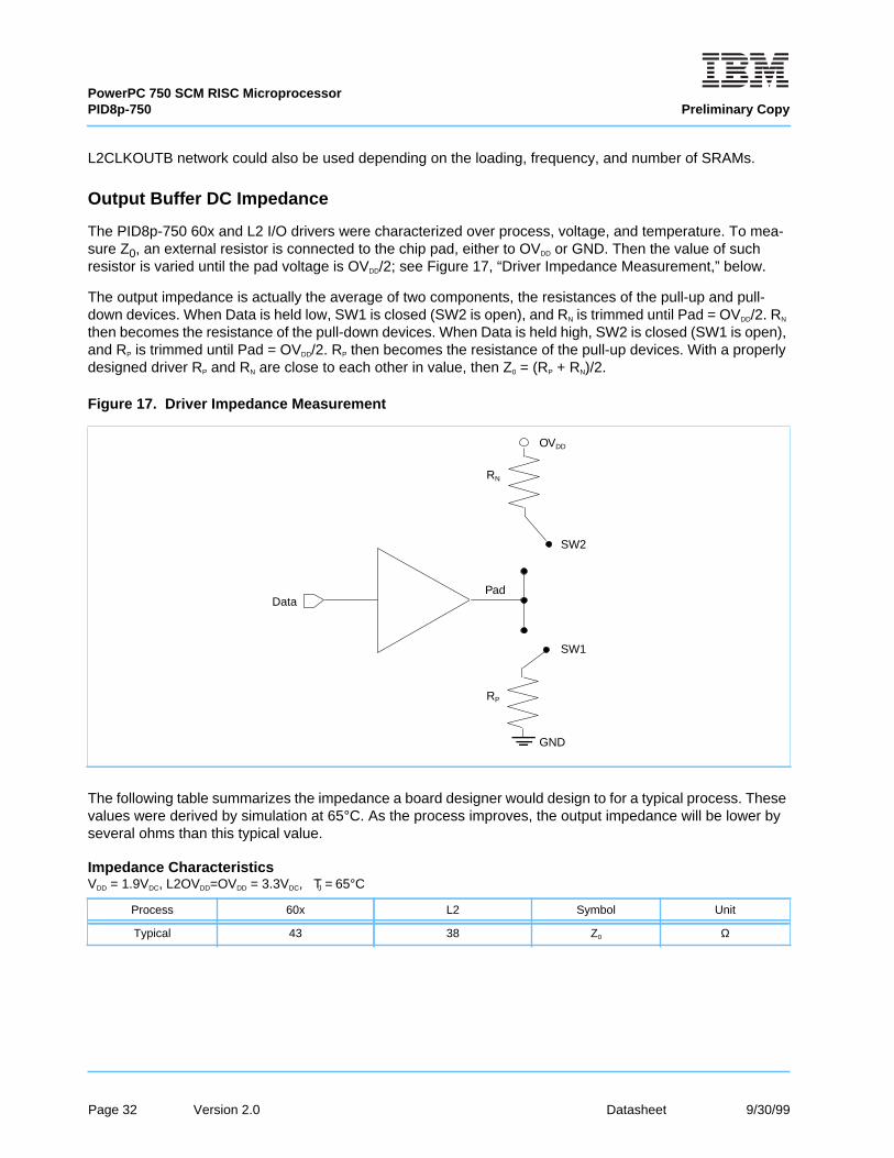
Output Buffer DC Impedance
The PID8p-750 60x and L2 I/O drivers were characterized over process, voltage, and temperature. To mea-sure Z0, an external resistor is connected to the chip pad, either to OVDD or GND. Then the value of suchresistor is varied until the pad voltage is OVDD/2; see Figure 17, “Driver Impedance Measurement,” below.
The output impedance is actually the average of two components, the resistances of the pull-up and pull-down devices. When Data is held low, SW1 is closed (SW2 is open), and RN is trimmed until Pad = OVDD/2. RN
then becomes the resistance of the pull-down devices. When Data is held high, SW2 is closed (SW1 is open),and RP is trimmed until Pad = OVDD/2. RP then becomes the resistance of the pull-up devices. With a properlydesigned driver RP and RN are close to each other in value, then Z0 = (RP + RN)/2.
The following table summarizes the impedance a board designer would design to for a typical process. Thesevalues were derived by simulation at 65°C. As the process improves, the output impedance will be lower byseveral ohms than this typical value.
Figure 17. Driver Impedance Measurement
Impedance CharacteristicsVDD = 1.9VDC, L2OVDD=OVDD = 3.3VDC, TJ = 65°C
Process 60x L2 Symbol Unit
Typical 43 38 Z0 Ω
Data
OVDD
RN
SW2
SW1
Pad
RP
GND
Page 32 Version 2.0 Datasheet 9/30/99
PowerPC 750 SCM RISC MicroprocessorPreliminary Copy PID8p-750
Pull-up / Pull-down Resistor Requirements
The PID8p-750 requires high-resistive (weak: 10KΩ) pull-up resistors on several control signals of the businterface to maintain the control signals in the negated state after they have been actively negated andreleased by the PID8p-750 or other bus masters. These signals are: TS, ABB, DBB, and ARTRY.
In addition, the PID8p-750 has one open-drain style output that requires a pull-up resistor (weak or stronger:4.7KΩ - 1- KΩ) if it is used by the system. This signal is: CKSTP_OUT.
If address or data parity is not used by the system, and the respective parity checking is disabled throughHID0, the input receivers for those pins are disabled. If all parity generation is disabled through HID0, than allparity checking should also be disabled through HID0. It is still recommended that the unused address ordata parity signals be tied high through pull up resistors to minimize noise on the package.
No pull-up resistors are normally required for the L2 interface.
HRESET Requirements
HRESET needs to be actively driven.
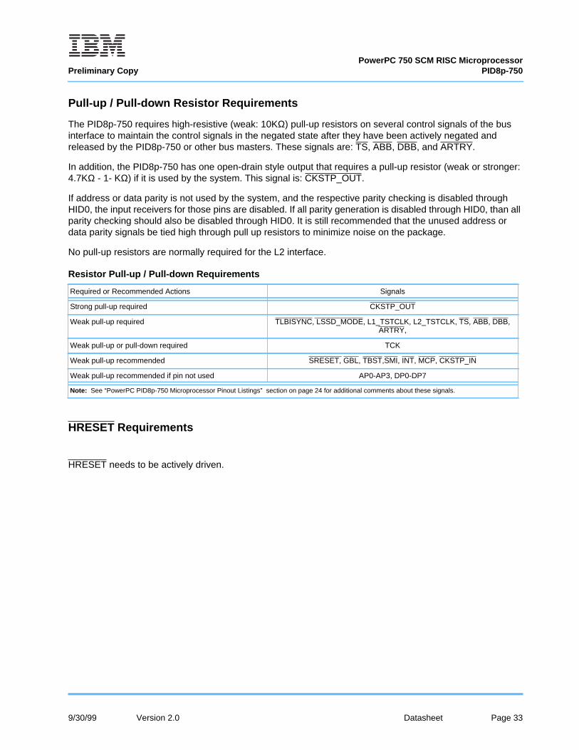
Resistor Pull-up / Pull-down Requirements
Required or Recommended Actions Signals
Strong pull-up required CKSTP_OUT
Weak pull-up required TLBISYNC, LSSD_MODE, L1_TSTCLK, L2_TSTCLK, TS, ABB, DBB,ARTRY,
Weak pull-up or pull-down required TCK
Weak pull-up recommended SRESET, GBL, TBST,SMI, INT, MCP, CKSTP_IN
Weak pull-up recommended if pin not used AP0-AP3, DP0-DP7
Note: See “PowerPC PID8p-750 Microprocessor Pinout Listings” section on page 24 for additional comments about these signals.
9/30/99 Version 2.0 Datasheet Page 33
PowerPC 750 SCM RISC MicroprocessorPID8p-750 Preliminary Copy
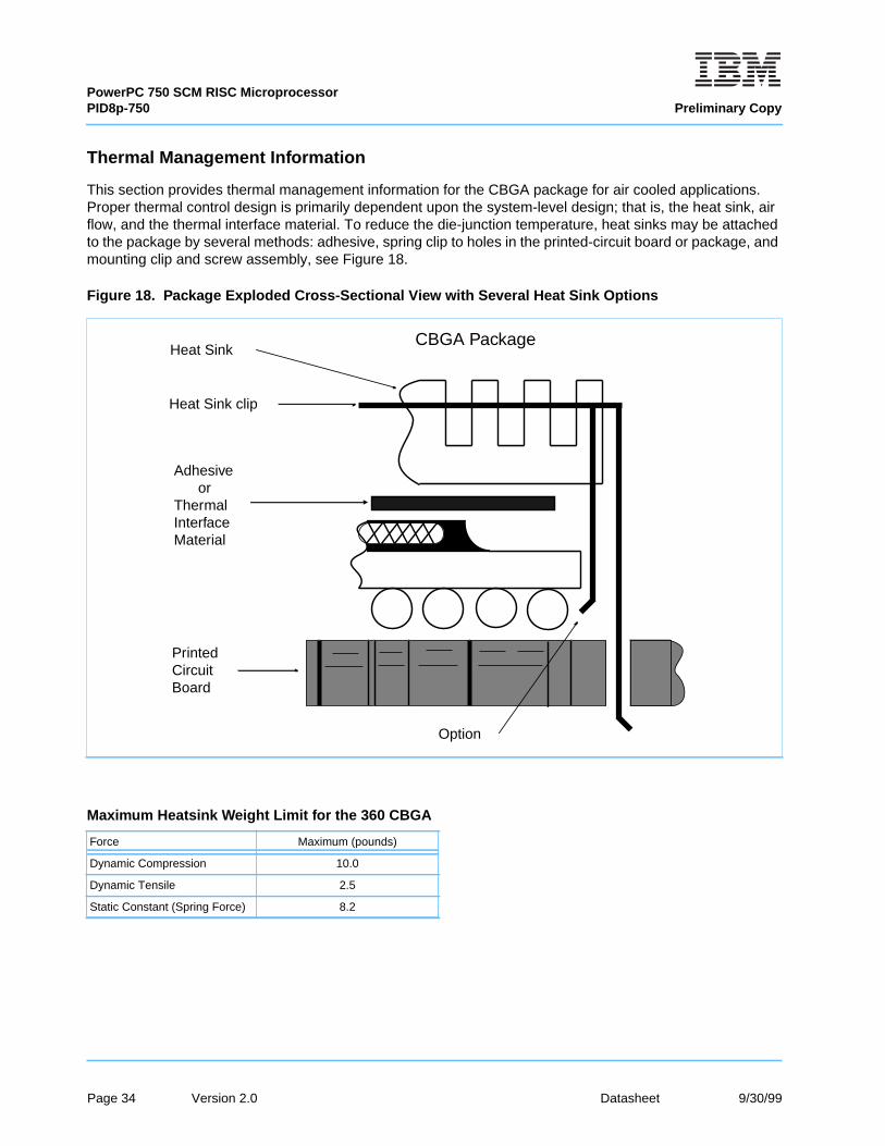
Thermal Management Information
This section provides thermal management information for the CBGA package for air cooled applications.Proper thermal control design is primarily dependent upon the system-level design; that is, the heat sink, airflow, and the thermal interface material. To reduce the die-junction temperature, heat sinks may be attachedto the package by several methods: adhesive, spring clip to holes in the printed-circuit board or package, andmounting clip and screw assembly, see Figure 18.
Figure 18. Package Exploded Cross-Sectional View with Several Heat Sink Options
Maximum Heatsink Weight Limit for the 360 CBGA
Force Maximum (pounds)
Dynamic Compression 10.0
Dynamic Tensile 2.5
Static Constant (Spring Force) 8.2
CBGA PackageHeat Sink
Heat Sink clip
Adhesive orThermalInterfaceMaterial
Printed
Option
CircuitBoard
Page 34 Version 2.0 Datasheet 9/30/99
PowerPC 750 SCM RISC MicroprocessorPreliminary Copy PID8p-750
The board designer can choose between several types of heat sinks to place on the PID8p-750. There areseveral commercially-available heat sinks for the PID8p-750 provided by the following vendors:
Chip Coolers, Inc. 800-227-0254 (USA/Canada)333 Strawberry Field Rd. 401-739-7600Warwick, RI 02887-6979
Thermalloy 214-243-43212021 W. Valley View LaneP.O. Box 810839Dallas, TX 75731
International Electronic Research Corporation (IERC) 818-842-7277135 W. Magnolia Blvd.Burbank, CA 91502
Aavid Engineering 603-528-3400One Kool PathLaconic, NH 03247-0440
Wakefield Engineering 617-245-590060 Audubon Rd.Wakefield, MA 01880
Ultimately, the final selection of an appropriate heat sink for the PID8p-750 depends on many factors, such asthermal performance at a given air velocity, spatial volume, mass, attachment method, assembly, and cost.
9/30/99 Version 2.0 Datasheet Page 35
PowerPC 750 SCM RISC MicroprocessorPID8p-750 Preliminary Copy
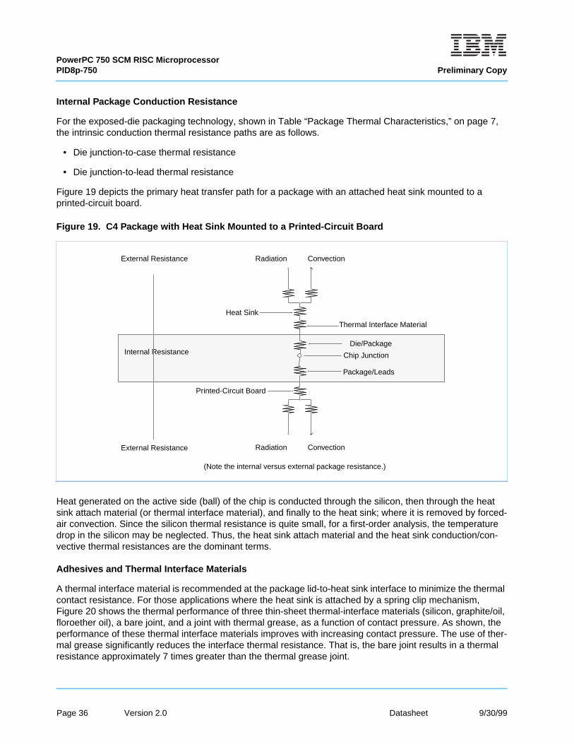
Internal Package Conduction Resistance
For the exposed-die packaging technology, shown in Table “Package Thermal Characteristics,” on page 7,the intrinsic conduction thermal resistance paths are as follows.
• Die junction-to-case thermal resistance
• Die junction-to-lead thermal resistance
Figure 19 depicts the primary heat transfer path for a package with an attached heat sink mounted to aprinted-circuit board.
Heat generated on the active side (ball) of the chip is conducted through the silicon, then through the heatsink attach material (or thermal interface material), and finally to the heat sink; where it is removed by forced-air convection. Since the silicon thermal resistance is quite small, for a first-order analysis, the temperaturedrop in the silicon may be neglected. Thus, the heat sink attach material and the heat sink conduction/con-vective thermal resistances are the dominant terms.
Adhesives and Thermal Interface Materials
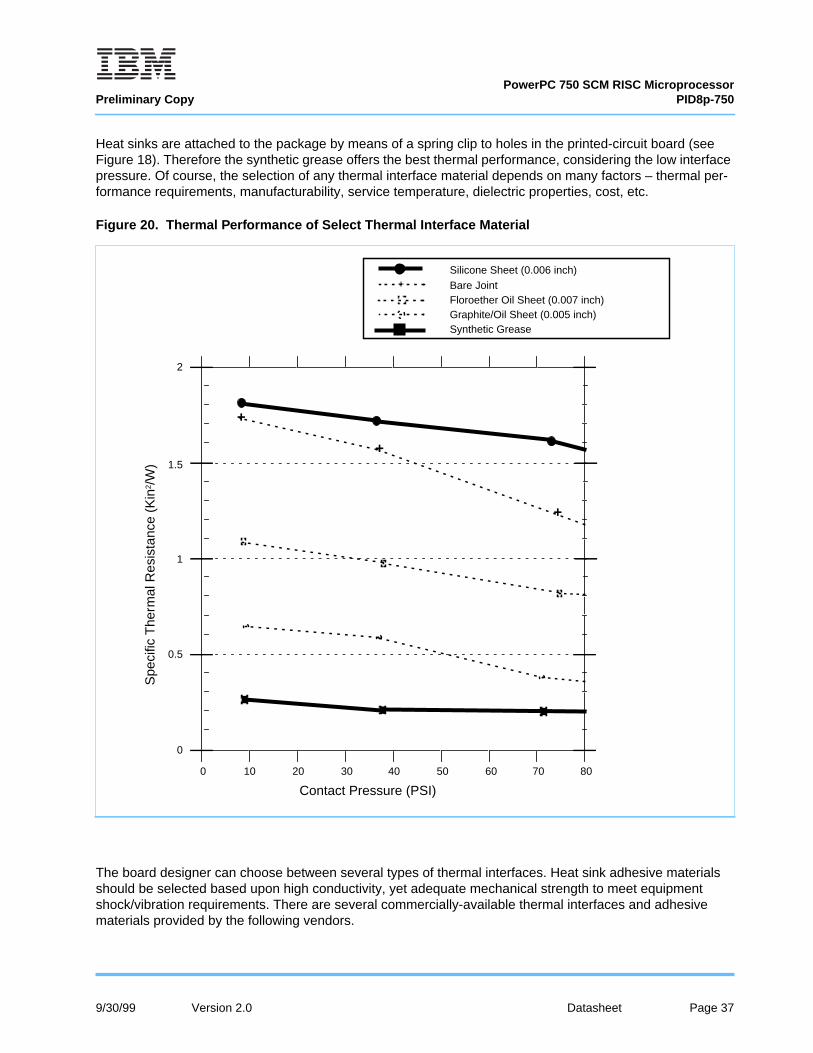
A thermal interface material is recommended at the package lid-to-heat sink interface to minimize the thermalcontact resistance. For those applications where the heat sink is attached by a spring clip mechanism,Figure 20 shows the thermal performance of three thin-sheet thermal-interface materials (silicon, graphite/oil,floroether oil), a bare joint, and a joint with thermal grease, as a function of contact pressure. As shown, theperformance of these thermal interface materials improves with increasing contact pressure. The use of ther-mal grease significantly reduces the interface thermal resistance. That is, the bare joint results in a thermalresistance approximately 7 times greater than the thermal grease joint.
Figure 19. C4 Package with Heat Sink Mounted to a Printed-Circuit Board
External Resistance
External Resistance
Internal Resistance
(Note the internal versus external package resistance.)
Radiation Convection
Radiation Convection
Heat Sink
Die/Package
Printed-Circuit Board
Thermal Interface Material
Package/Leads
Chip Junction
Page 36 Version 2.0 Datasheet 9/30/99
PowerPC 750 SCM RISC MicroprocessorPreliminary Copy PID8p-750
Heat sinks are attached to the package by means of a spring clip to holes in the printed-circuit board (seeFigure 18). Therefore the synthetic grease offers the best thermal performance, considering the low interfacepressure. Of course, the selection of any thermal interface material depends on many factors – thermal per-formance requirements, manufacturability, service temperature, dielectric properties, cost, etc.
The board designer can choose between several types of thermal interfaces. Heat sink adhesive materialsshould be selected based upon high conductivity, yet adequate mechanical strength to meet equipmentshock/vibration requirements. There are several commercially-available thermal interfaces and adhesivematerials provided by the following vendors.
Figure 20. Thermal Performance of Select Thermal Interface Material
Spe
cific
The
rmal
Res
ista
nce
(Kin
2 /W
)
0
0.5
1
1.5
2
0
10 20 30 40 50 60 70 80
Contact Pressure (PSI)
+
+
+
Silicone Sheet (0.006 inch)Bare JointFloroether Oil Sheet (0.007 inch)Graphite/Oil Sheet (0.005 inch)Synthetic Grease
+
9/30/99 Version 2.0 Datasheet Page 37
PowerPC 750 SCM RISC MicroprocessorPID8p-750 Preliminary Copy
Dow-Corning Corporation 517-496-4000Dow-Corning Electronic MaterialsP.O. Box 0997Midland, MI 48686-0997
Chomerics, Inc. 617-935-485077 Dragon CourtWoburn, MA 01888-4850
Thermagon, Inc. 216-741-76593256 West 25th StreetCleveland, OH 44109-1668
Loctite Corporation 860-571-51001001 Trout Brook CrossingRocky Hill, CT 06067
AI Technology (e.g. EG7655) 609-882-23321425 Lower Ferry RoadTrent, NJ 08618
The following section provides a heat sink selection example using one of the commercially available heatsinks.
Heat Sink Selection Example
For preliminary heat sink sizing, the die-junction temperature can be expressed as follows.
TJ = TA + TR + (θJC + θINT + θSA) × PD
Where :TJ is the die-junction temperatureTA is the inlet cabinet ambient temperatureTR is the air temperature rise within the system cabinetθJC is the junction-to-case thermal resistanceθINT is the thermal resistance of the thermal interface materialθSA is the heat sink-to-ambient thermal resistancePD is the power dissipated by the device
Typical die-junction temperatures (TJ) should be maintained less than the value specified in Table “PackageThermal Characteristics,” on page 7. The temperature of the air cooling the component greatly depends uponthe ambient inlet air temperature and the air temperature rise within the computer cabinet. An electronic cab-inet inlet-air temperature (TA) may range from 30 to 40°C. The air temperature rise within a cabinet (TR) maybe in the range of 5 to 10°C. The thermal resistance of the interface material (θINT) is typically about 1°C/W.Assuming a TA of 30°C, a TR of 5°C, a CBGA package θJC = 0.03, and a power dissipation (PD) of 5.0 watts, thefollowing expression for TJ is obtained.
Die-junction temperature: TJ = 30°C + 5°C + (0.03°C/W +1.0°C/W + θSA) × 5W
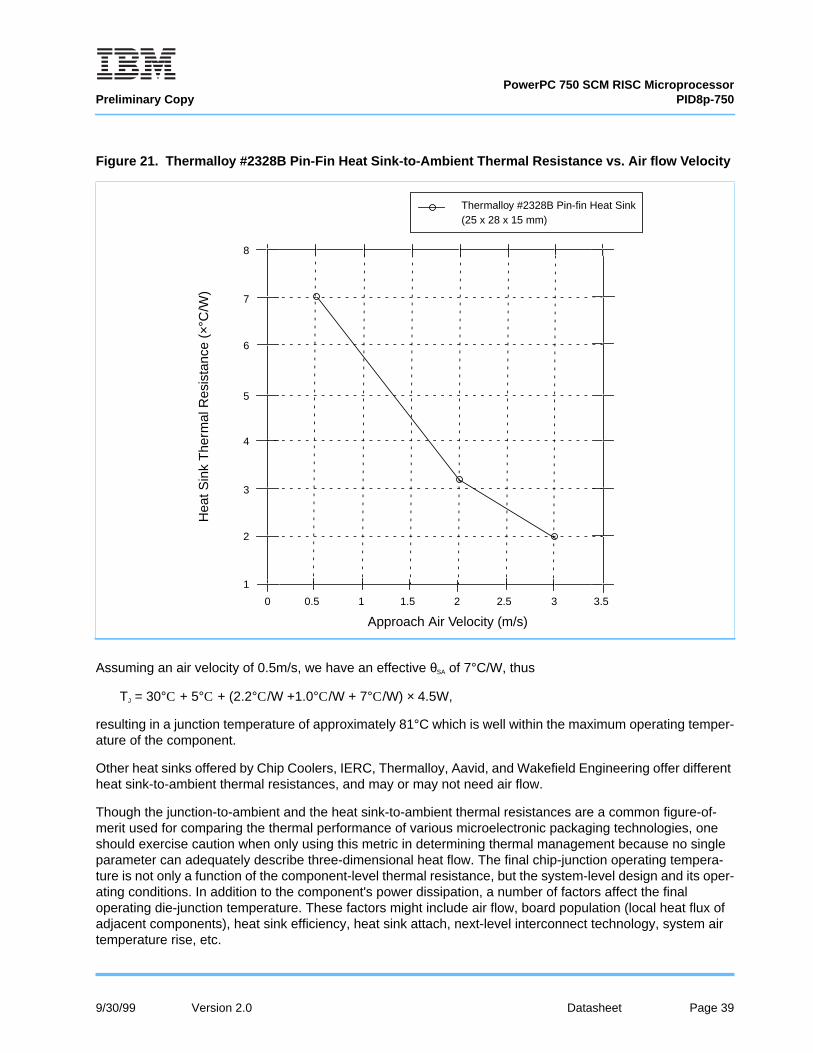
For a Thermalloy heat sink #2328B, the heat sink-to-ambient thermal resistance (θSA) versus air flow velocityis shown in Figure 21.
Page 38 Version 2.0 Datasheet 9/30/99
PowerPC 750 SCM RISC MicroprocessorPreliminary Copy PID8p-750
Assuming an air velocity of 0.5m/s, we have an effective θSA of 7°C/W, thus
TJ = 30°C + 5°C + (2.2°C/W +1.0°C/W + 7°C/W) × 4.5W,
resulting in a junction temperature of approximately 81°C which is well within the maximum operating temper-ature of the component.
Other heat sinks offered by Chip Coolers, IERC, Thermalloy, Aavid, and Wakefield Engineering offer differentheat sink-to-ambient thermal resistances, and may or may not need air flow.
Though the junction-to-ambient and the heat sink-to-ambient thermal resistances are a common figure-of-merit used for comparing the thermal performance of various microelectronic packaging technologies, oneshould exercise caution when only using this metric in determining thermal management because no singleparameter can adequately describe three-dimensional heat flow. The final chip-junction operating tempera-ture is not only a function of the component-level thermal resistance, but the system-level design and its oper-ating conditions. In addition to the component's power dissipation, a number of factors affect the finaloperating die-junction temperature. These factors might include air flow, board population (local heat flux ofadjacent components), heat sink efficiency, heat sink attach, next-level interconnect technology, system airtemperature rise, etc.
Figure 21. Thermalloy #2328B Pin-Fin Heat Sink-to-Ambient Thermal Resistance vs. Air flow Velocity
Approach Air Velocity (m/s)
Hea
t Sin
k T
herm
al R
esis
tanc
e (×
°C/W
)
1
2
3
4
5
6
7
8
0 0.5 1 1.5 2 2.5 3 3.5
Thermalloy #2328B Pin-fin Heat Sink(25 x 28 x 15 mm)
9/30/99 Version 2.0 Datasheet Page 39
PowerPC 750 SCM RISC MicroprocessorPID8p-750 Preliminary Copy
Ordering Information
This section provides the part numbering nomenclature for the PID8p-750. Note that the individual part num-bers correspond to a maximum processor core frequency. For available frequencies, contact your local IBMsales office.
In addition to the processor frequency and bus ratio, the part numbering scheme also consists of a part mod-ifier. The part modifier allows for the availability of future enhanced parts (that is, lower voltage, lower power,higher performance, etc.).
Each part number also contains a revision code. This refers to the die mask revision number and is specifiedin the part numbering scheme for identification purposes only.
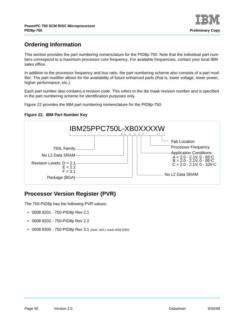
Figure 22 provides the IBM part numbering nomenclature for the PID8p-750.
Processor Version Register (PVR)
The 750-PID8p has the following PVR values:
• 0008 8201 - 750-PID8p Rev 2.1
• 0008 8202 - 750-PID8p Rev 2.2
• 0008 8300 - 750-PID8p Rev 3.1 (Note: dd3.1 reads 0008 8300)
Figure 22. IBM Part Number Key
750L Family
IBM25PPC750L-XB0XXXXW
Package (BGA)
Revision Levels: D = 2.1
No L2 Data SRAM
No L2 Data SRAM
Application Conditions:
Fab LocationProcessor Frequency
A = 2.0 - 2.1V, 0 - 65°CB = 2.0 - 2.1V, 0 - 85°CC = 2.0 - 2.1V, 0 - 105°C
E = 2.2F = 3.1
Page 40 Version 2.0 Datasheet 9/30/99
PowerPC 750 SCM RISC MicroprocessorPreliminary Copy PID8p-750
9/30/99 Version 2.0 Datasheet Page 41
© International Business Machines Corporation 1998
Printed in the United States of America
9/30/99
All Rights Reserved
The information contained in this document is subject to change without notice. The products described in this documentare NOT intended for use in implantation or other life support applications where malfunction may result in injury or death topersons. The information contained in this document does not affect or change IBM’s product specifications or warranties.Nothing in this document shall operate as an express or implied license or indemnity under the intellectual property rights ofIBM or third parties. All information contained in this document was obtained in specific environments, and is presented asillustration. The results obtained in other operating environments may vary.
While the information contained herein is believed to be accurate, such information is preliminary, and should not be reliedupon for accuracy or completeness, and no representations or warranties of accuracy or completeness are made.
THE INFORMATION CONTAINED IN THIS DOCUMENT IS PROVIDED ON AN “AS IS” BASIS. In no event will IBM be lia-ble for any damages arising directly or indirectly from any use of the information contained in this document.
IBM Microelectronics Division1580 Route 52, Bldg. 504Hopewell Junction, NY12533-6531
The IBM home page can be found at http://www.ibm.com
The IBM Microelectronics Division home page can be found at http://www.chips.ibm.com