Organic-Organic Semiconductor Interfaces for Molecular Electronic

Potentiometry on organic semiconductor devices
Citation for published version (APA):Charrier, D. S. H. (2009). Potentiometry on organic semiconductor devices. Eindhoven: Technische UniversiteitEindhoven. https://doi.org/10.6100/IR652483
DOI:10.6100/IR652483
Document status and date:Published: 01/01/2009
Document Version:Publisher’s PDF, also known as Version of Record (includes final page, issue and volume numbers)
Please check the document version of this publication:
• A submitted manuscript is the version of the article upon submission and before peer-review. There can beimportant differences between the submitted version and the official published version of record. Peopleinterested in the research are advised to contact the author for the final version of the publication, or visit theDOI to the publisher's website.• The final author version and the galley proof are versions of the publication after peer review.• The final published version features the final layout of the paper including the volume, issue and pagenumbers.Link to publication
General rightsCopyright and moral rights for the publications made accessible in the public portal are retained by the authors and/or other copyright ownersand it is a condition of accessing publications that users recognise and abide by the legal requirements associated with these rights.
• Users may download and print one copy of any publication from the public portal for the purpose of private study or research. • You may not further distribute the material or use it for any profit-making activity or commercial gain • You may freely distribute the URL identifying the publication in the public portal.
If the publication is distributed under the terms of Article 25fa of the Dutch Copyright Act, indicated by the “Taverne” license above, pleasefollow below link for the End User Agreement:
www.tue.nl/taverne
Take down policyIf you believe that this document breaches copyright please contact us at:
providing details and we will investigate your claim.
Download date: 07. Feb. 2020
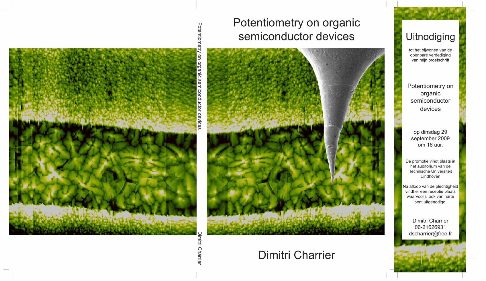
Potentiometry on organicsemiconductor devices
Dimitri Charrier
Potentiom
etry on organic semiconductor devices D
imitri C
harrier
Uitnodigingtot het bijwonen van deopenbare verdedigingvan mijn proefschrift
Potentiometry onorganic
semiconductordevices
op dinsdag 29september 2009
om 16 uur.
De promotie vindt plaats inhet auditorium van de
Technische Universiteit Eindhoven
Na afloop van de plechtigheidvindt er een receptie plaatswaarvoor u ook van harte
bent uitgenodigd.
Dimitri Charrier06-21626931
Potentiometry on organic semiconductor devices
PROEFSCHRIFT
ter verkrijging van de graad van doctor aan de Technische Universiteit Eindhoven,
op gezag van de rector magnificus, prof.dr.ir. C.J. van Duijn,
voor een commissie aangewezen door het College voor Promoties
in het openbaar te verdedigen op dinsdag 29 september 2009 om 16.00 uur
door
Dimitri Sébastien Hans Charrier
geboren te Privas, Frankrijk
Dit proefschrift is goedgekeurd door de promotor: prof.dr.ir. R.A.J. Janssen Copromotor: dr.ir. M. Kemerink A catalogue record is available from the Eindhoven University of Technology Library. Charrier, Dimitri Sébastien Hans Potentiometry on organic semiconductor devices / by Dimitri Charrier. - Eindhoven: Technische Universiteit Eindhoven, 2009. Proefschrift. ISBN 978-90-386-2004-6
NUR 926
Trefwoorden: organische halfgeleiders / organische veld-effect transistor / potentiometrie / Kelvin scanning probe microscoop / modelleren / recombinatie breedte / overdracht functie / scanning tunneling microscoop / actuator Subject headings: organic semiconductors / organic field effect transistor / potentiometry / scanning Kelvin probe microscope / modeling / recombination width / transfer function / scanning tunneling microscope / actuator Printed by Gildeprint Drukkerijen in Enschede This research was financially supported by NanoNed (NanoNed is the Dutch nanotechnology initiative by the Ministry of Economic Affairs).

iii
Contents
1. Introduction 1
1.1 Context . . . . . . . . . . . . . . . . . . . . . . . . . . . . . . . . . . . . . . . . . . . . . . . . . . . . . . . . . . 1 1.2 Materials used in this thesis . . . . . . . . . . . . . . . . . . . . . . . . . . . . . . . . . . . . . . . . . . 2 1.3 Organic field effect transistors . . . . . . . . . . . . . . . . . . . . . . . . . . . . . . . . . . . . . . . . 3 1.4 Scanning Kelvin probe microscopy . . . . . . . . . . . . . . . . . . . . . . . . . . . . . . . . . . . 11 1.5 Scanning Kelvin probe microscopy on oFETs . . . . . . . . . . . . . . . . . . . . . . . . . . .14 1.6 Scopes of the thesis . . . . . . . . . . . . . . . . . . . . . . . . . . . . . . . . . . . . . . . . . . . . . . . .17 1.7 References and notes . . . . . . . . . . . . . . . . . . . . . . . . . . . . . . . . . . . . . . . . . . . . . . .18
2. Real versus measured surface potentials in scanning Kelvin probe
microscopy 23
2.1 Introduction . . . . . . . . . . . . . . . . . . . . . . . . . . . . . . . . . . . . . . . . . . . . . . . . . . . . . .23 2.2 Experimental scanning Kelvin probe microscope results . . . . . . . . . . . . . . . . . . .24 2.3 Simulation of scanning Kelvin probe microscope . . . . . . . . . . . . . . . . . . . . . . . . 27 2.4 Conclusion . . . . . . . . . . . . . . . . . . . . . . . . . . . . . . . . . . . . . . . . . . . . . . . . . . . . . . 33 2.5 Materials and methods . . . . . . . . . . . . . . . . . . . . . . . . . . . . . . . . . . . . . . . . . . . . . 33 2.6 References and notes . . . . . . . . . . . . . . . . . . . . . . . . . . . . . . . . . . . . . . . . . . . . . . .34
3. On the width of the recombination zone in organic light emitting field effect
transistors 37
3.1 Introduction . . . . . . . . . . . . . . . . . . . . . . . . . . . . . . . . . . . . . . . . . . . . . . . . . . . . . .37 3.2 Analytical model of recombination width . . . . . . . . . . . . . . . . . . . . . . . . . . . . . . 38 3.3 Recombination width of a NiDT field-effect transistor . . . . . . . . . . . . . . . . . . . . 42 3.4 Conclusion . . . . . . . . . . . . . . . . . . . . . . . . . . . . . . . . . . . . . . . . . . . . . . . . . . . . . . 44 3.5 References and notes . . . . . . . . . . . . . . . . . . . . . . . . . . . . . . . . . . . . . . . . . . . . . . 44
4. Bimolecular recombination in ambipolar organic field effect transistors 47
4.1 Introduction. . . . . . . . . . . . . . . . . . . . . . . . . . . . . . . . . . . . . . . . . . . . . . . . . . . . . . 47 4.2 Materials and methods . . . . . . . . . . . . . . . . . . . . . . . . . . . . . . . . . . . . . . . . . . . . . 49 4.3 Results and discussion . . . . . . . . . . . . . . . . . . . . . . . . . . . . . . . . . . . . . . . . . . . . . 51 4.4 Conclusion . . . . . . . . . . . . . . . . . . . . . . . . . . . . . . . . . . . . . . . . . . . . . . . . . . . . . . 54 4.5 References and notes . . . . . . . . . . . . . . . . . . . . . . . . . . . . . . . . . . . . . . . . . . . . . . .54
iv
5. Scanning tunneling microscopy via the accumulation layer of p-type organic field effect transistors 57
5.1 Introduction . . . . . . . . . . . . . . . . . . . . . . . . . . . . . . . . . . . . . . . . . . . . . . . . . . . . . .57 5.2 Materials and methods . . . . . . . . . . . . . . . . . . . . . . . . . . . . . . . . . . . . . . . . . . . . . 58 5.3 Results and discussion . . . . . . . . . . . . . . . . . . . . . . . . . . . . . . . . . . . . . . . . . . . . . 60 5.4 Conclusion . . . . . . . . . . . . . . . . . . . . . . . . . . . . . . . . . . . . . . . . . . . . . . . . . . . . . . 65 5.5 References and notes . . . . . . . . . . . . . . . . . . . . . . . . . . . . . . . . . . . . . . . . . . . . . . .65
6. Giant out-of-plane ambient actuation of poly(3,4-ethylenedioxythiophene) :
poly(styrenesulfonate) thin films 67
6.1 Introduction . . . . . . . . . . . . . . . . . . . . . . . . . . . . . . . . . . . . . . . . . . . . . . . . . . . . . .67 6.2 Results . . . . . . . . . . . . . . . . . . . . . . . . . . . . . . . . . . . . . . . . . . . . . . . . . . . . . . . . . .68
6.2.1 Out-of-plane actuation at the anode . . . . . . . . . . . . . . . . . . . . . . . . . . . . . 68 6.2.2 Depletion and morphology changes in the channel . . . . . . . . . . . . . . . . . 71 6.2.3 Lack of volume conservation . . . . . . . . . . . . . . . . . . . . . . . . . . . . . . . . . . 73 6.2.4 Reversibility of actuation . . . . . . . . . . . . . . . . . . . . . . . . . . . . . . . . . . . . . 74 6.2.5 Role of humidity in actuation and stability . . . . . . . . . . . . . . . . . . . . . . . .76 6.2.6 Surface potential measurements . . . . . . . . . . . . . . . . . . . . . . . . . . . . . . . .78
6.3 Discussion . . . . . . . . . . . . . . . . . . . . . . . . . . . . . . . . . . . . . . . . . . . . . . . . . . . . . . .80 6.4 Conclusion . . . . . . . . . . . . . . . . . . . . . . . . . . . . . . . . . . . . . . . . . . . . . . . . . . . . . . 85 6.5 Experimental . . . . . . . . . . . . . . . . . . . . . . . . . . . . . . . . . . . . . . . . . . . . . . . . . . . . .85 6.6 References and notes . . . . . . . . . . . . . . . . . . . . . . . . . . . . . . . . . . . . . . . . . . . . . . .86
Summary 89 Samenvatting 93 Acknowledgements 97 Curriculum Vitae 101
Chapter 1
Introduction
1.1 Context
The field of organic electronics is rapidly maturing, as witnessed by, e.g.,
hundreds of organic transistors performing complex logical operations1,2 and organic
materials forming the heart of both rigid and flexible displays, based on various
operational principles like e-ink3 and fluorescence or phosphorescence.4 Nevertheless,
many important questions are still open and will likely require novel or improved
measurement schemes to be answered. The goal of this chapter is to give a short
introduction on the functioning and metrology of an important organic device, the organic
field effect transistor (oFET), which is the building block of logical circuits.
Recent years showed an intense and competitive research on measuring and
modeling the functionality of oFETs. The most commonly used technique, measurement
of the transfer and output curves, suffers from the drawback that what goes on in the
channel has to be deduced from the behavior at the terminals. In other words, there is a
‘black box’ problem, which evidently asks for ways to probe the operational channel. To
physically access the channel, which is typically a few to a few tens of microns long,
scarce technical options are available. Far-field optical methods are limited in lateral
resolution by diffraction effects to at best half the wavelength used. Near-field optical
techniques may have a sub-100 nm resolution, but do so at the cost of much weaker
signals. In all cases, the most relevant information is electrical in nature, and the
associated optical signatures are often very small but measurable. E.g. charge modulation
spectroscopy can be used to probe the excitation at the dielectric/semiconductor interface
through a transparent layer.5 Also Stark shifts can also be measured in situ and yield
information on (local) electric fields.6,7 In comparison, scanning probe microscopy (SPM)
1
is usually far more accurate in terms of lateral resolution, which may be below the single
atom level, depending on conditions, sample and probing scheme. Among the wide
variety of SPM techniques, the most logical choice is scanning Kelvin probe microscopy
or SKPM. This technique allows one to measure the local potential inside the oFET
channel, which can quantitatively, and in principle directly, be compared to transport
models. Moreover, SKPM is a standard option on most modern atomic force microscopes
(AFM).
Not surprisingly, SKPM is nowadays the most commonly used tool for looking at
the channel potential. However, the SKPM technique still suffers from limitations in
resolution due to the intrinsic capacitive coupling between the entire probe, of which the
tip apex is only the extreme part, and the entire device. As a consequence the measured
surface potential needs deepened analysis before quantitative, or even qualitative,
comparison to theoretical predictions can be made. In this thesis, such an analysis was
performed which enabled us to use the SKPM technique to investigate the physics of
oFETs.
1.2 Materials used in this thesis
The list of organic semiconductor materials that is used in the active layer of
oFETs is virtually endless, and still growing. Of these, we focused on two prototypical
materials, shown in Fig. 1 a) and b). Pentacene (PC) is taken as reference molecule
because of its ubiquity and its high performance in p-type oFETs, see Fig. 1 a). The high
performance in this context refers to the relatively high mobility of holes in the
crystalline phase, which can be as high as 1.4 cm2/Vs.8 Thermally evaporated films are
typically polycrystalline, with the grain boundaries reducing the mobility to typically 0.1
cm2/Vs.9 Nickel dithiolene (NiDT) is a small metalorganic dye that was recently found to
show ambipolar behavior in oFETs on SiO2 substrates under ambient conditions, see Fig.
1 b).10 Poly(3,4-ethylenedioxythiophene) : poly(styrenesulfonate) (PEDOT:PSS) (Fig. 1
c)) is a doped small-bandgap semiconductor and hence not applicable as active layer in
an oFET, but it is the most likely candidate for replacing metal electrodes in all-plastic
2
1. Introduction
and transparent devices because of its plasticity, transparency and its quasi metallic
conductivity. Despite the fact that it is one of the most used materials in the field, it can
still show very surprising behavior, as shown in Chapter 6.
Fig. 1. Materials studied in this thesis, a) pentacene (PC), b) nickel dithiolene (NiDT),
and c) poly(3,4-ethylenedioxythiophene):poly(styrenesulfonate) (PEDOT:PSS).
1.3 Organic field effect transistors
One of the reasons motivating the effort put into improving performance and
reliability of oFETs is the hope for lower production costs than Si technology as soon as
large area devices can be produced in a roll-to-roll way. Another advantage may be the
higher plasticity and robustness than amorphous Si (a-Si).
organic semiconductor
gate
source drain
dielectric (εr)
L
d - - - - - - - - - - - - - - - -
+ + + + + + + + + + +
Vsg
Vsd
Fig. 2. Cross-section drawing of a typical organic field effect transistor (oFET), with an
organic semiconductor, electrically driven by the source, drain, and gate electrodes.
Positive charge (hole) accumulation occurs throughout the channel when |Vsg| > |Vsd| and
Vsg < 0.
3
A potential application then is the backplane of active matrix displays, where
organic circuitry should replace the already existing flexible a-Si. An oFET is formed by
an organic semiconductor with three electrical terminals: a gate, a source and a drain, see
Fig. 2. The space between source and drain, called the channel, has a length L and a width
W. While the organic semiconductive layer is in direct contact with the source and drain
electrodes, the gate electrode is connected to it via a dielectric spacer (εr > 1) of thickness
d. When a gate bias is applied, charges accumulate at the organic
semiconductor/dielectric interface, like in a capacitor. Since the carriers are mobile in the
semiconductor, the channel becomes conductive. Then, at finite source-drain bias, a
source-drain current will flow. The threshold voltage Vth defines the gate voltage at which
a conductive channel between source and drain is formed.
The carrier density in the organic layer increases with the source-gate bias Vsg
allowing an increasing source-drain current Isd to flow at a fixed source-drain bias Vsd.
When Vsg - Vth > Vsd, the transistor is in the linear regime. In this regime, the charge
density in the accumulation layer is roughly constant, and the current is linear in both Vsg
and Vsd.11 When |Vsg - Vth| < |Vsd|, the transistor is in the saturation regime, which is
characterized by Isd being independent of Vsd. A depletion region is present at the drain
side of the channel in this regime.
The field effect mobility µ (cm2/Vs) is one of the main performance indicators of
oFETs and can be extracted by means of transport measurements, e.g. via measurement
of the transfer characteristic Isd(Vsg). The mobility µ in the linear regime can be written as
sgsdrlin dVdIWd /)/( 20εεµ = where ε0 = 8.854 × 10⁻¹² F/m. In organic single crystals,
mobilities above 10 cm2/Vs have been achieved,8,12 which surpass mobilities in
amorphous silicon thin film transistors. The single crystals have the advantage to show
the intrinsic mobilities while polycrystalline materials show a lower mobility (~0.1
cm2/Vs) that is limited by the grain boundaries. In that case, advanced four-point-probe
measurements can still enable one to estimate the intrinsic mobility.9 For polymer
materials that show good ordering properties, the highest reported mobilities are around
0.2 cm2/Vs for poly(3-hexylthiophene) (P3HT)13 and 0.72 cm2/Vs for poly(2,5-bis(3-
alkylthiophen-2-yl)thieno[3,2-b]thiophene) (PBTTT).14 In strongly disordered polymers
like most poly(p-phenylene vinylene) (PPV) derivatives, mobilities are typically 10-5
4

1. Introduction
cm2/Vs and below.15 To date, the record mobility in disordered polymers was obtained at
0.85 cm2/Vs for poly{[N,N’-bis(2-octyldodecyl)-naphthalene-1,4,5,8-bis(dicarboximide)-
2,6-diyl]-alt-5,5’-(2,2’-bithiophene)} (P(NDI2OD-T2)).16
The first polycrystalline (polythiophene) oFETs, as described by Tsumura et al.,17
showed a relatively poor performance. Nevertheless they are very suited to gain
understanding of the typical physical limitations of oFETs: contact resistance, gate
dielectric problems, and a low intrinsic mobility. Below, these three issues will be
discussed in more detail.
The contact resistance, i.e. the injection barrier between the metallic electrode
and the semiconductor can be estimated by measuring the longitudinal resistance as a
function of channel length. The resistance is then obtained by extrapolating the device
resistance to channel length equal zero. Typically found contact resistances for
sexithiophene (6 T) on Au electrodes are in the range of 105-106 �.18
Gate dielectric. Since the flexible substrates are in state of development, most
organic transistors use SiO2 (εr = 3.9) on highly doped Si as gate dielectric. This is,
amongst others, due to an easier patterning of the metallic electrodes than on a polymer
dielectric, although some organic dielectrics have a good dielectric constant and show
low leakage currents to the gate.19 The morphology of gate dielectric and the interfacial
chemical interaction with the semiconductor play an important role in the apparent
mobility. Hysteresis, charge trapping, and nonzero threshold voltages are commonly
attributed to the gate dielectric. A lot of effort is given to improve the transport at the
dielectric/semiconductor interface, which enabled a gain by several orders of magnitude
in mobility.20 Note that some free-dielectric (εr = 1) oFETs have also been realized, using
vacuum as a spacer.21 They have the advantage to circumvent the charge trapping at the
organic semiconductor/dielectric interface.
Low mobility. From conjugated polymers to small molecules, the recent strategy
to obtain high mobility and solution-processed oFETs is in general to have soluble
materials, highly microcrystalline layers, and a high density of states. Sirringhaus22 gives
an overview of such high performance materials. The regioregular P3HT reaches high
field effect mobilities 0.1-0.3 cm2/Vs.23,24 Several routes allow small molecules to be
solution processible such as precursor routes, side chain substitution and liquid crystalline
5
molecule. For instance, pentacene precursors showed mobilities from 0.01 to 0.8
cm2/Vs25,26 after thermal conversion at 150-200 °C. The high density of states is obtained
with well-designed materials leading to strong �-� interchain interactions. The correlation
between transport properties and morphology is often completed by X-ray diffraction
giving molecular packing within the randomly oriented microcrystals.
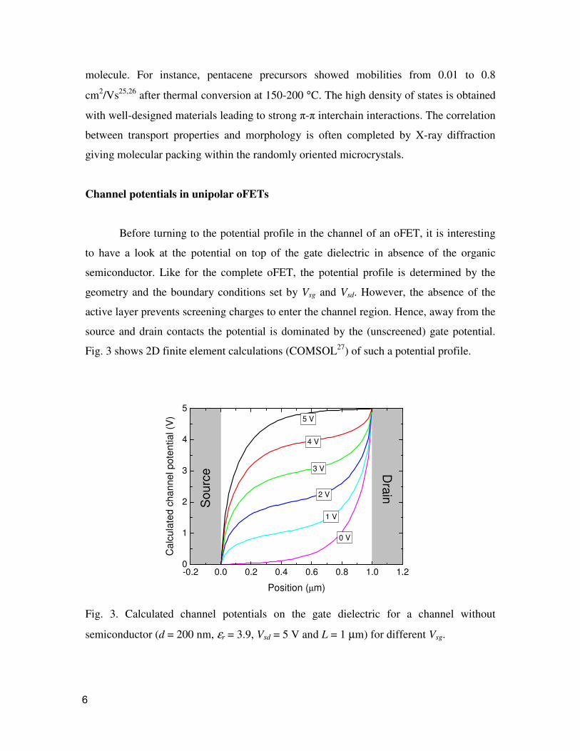
Channel potentials in unipolar oFETs
Before turning to the potential profile in the channel of an oFET, it is interesting
to have a look at the potential on top of the gate dielectric in absence of the organic
semiconductor. Like for the complete oFET, the potential profile is determined by the
geometry and the boundary conditions set by Vsg and Vsd. However, the absence of the
active layer prevents screening charges to enter the channel region. Hence, away from the
source and drain contacts the potential is dominated by the (unscreened) gate potential.
Fig. 3 shows 2D finite element calculations (COMSOL27) of such a potential profile.
-0.2 0.0 0.2 0.4 0.6 0.8 1.0 1.20
1
2
3
4
5
Drain
5 V
4 V
3 V
2 V
1 V
0 V
Cal
cula
ted
chan
nel p
oten
tial (
V)
Position (µm)
Sou
rce
Fig. 3. Calculated channel potentials on the gate dielectric for a channel without
semiconductor (d = 200 nm, εr = 3.9, Vsd = 5 V and L = 1 µm) for different Vsg.
6
1. Introduction
As soon as a hole or electron transporting material is present, the gate bias causes
accumulation of charges in the lowest unoccupied molecular orbital (LUMO) (for Vsg >
0) or highest occupied molecular orbital (HOMO) (for Vsg < 0) of the organic
semiconductor. Making approximations,11 such as the gradual channel approximation, no
contact resistance, no depletion, no diffusion and assuming an exponential density of
states, it is possible to calculate the analytical channel potential V(x) (Eq. (1)). The
gradual channel approximation supposes the electric field induced by the gate is much
larger than the field induced by the electrodes. In practice, this is valid for large channel
lengths. In oFETs, an exponential density of states is commonly assumed28 and has the
advantage to be analytically treatable. From the current continuity equation one then
obtains:
{ } ββββ /1])()[(/)()( thsgsdthsgthsgthsg VVVVVLxVVVVxV +−−+−−+−+−= (1)
with TT /2 0=β . T0 is a measure of the width of the exponential density of states and T is
the absolute temperature.
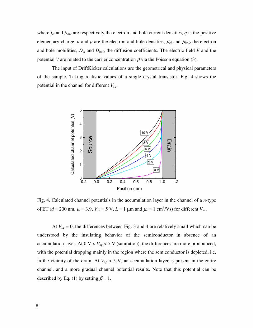
In case depletion regions are present, analytical calculations are no longer
possible and numerical models are required to calculate the channel potential. Within our
group a program (DriftKicker) has been developed which enables numerical calculations
of channel and surface potentials (the difference will be discussed below) on basis of the
coupled drift/diffusion (Eq. (2)) and Poisson (Eq. (3)) equations. In 1 dimension, these
are:
total el hole
el el el
hole hole hole
j j j
dnj qn E qD
dxdp
j qp E qDdx
µ
µ
= +
= +
= −
(2)
rdxVd
dxdE
εερ0
2
2
=−= (3)
7
where jel and jhole are respectively the electron and hole current densities, q is the positive
elementary charge, n and p are the electron and hole densities, µel and µhole the electron
and hole mobilities, Del and Dhole the diffusion coefficients. The electric field E and the
potential V are related to the carrier concentration ρ via the Poisson equation (3).
The input of DriftKicker calculations are the geometrical and physical parameters
of the sample. Taking realistic values of a single crystal transistor, Fig. 4 shows the
potential in the channel for different Vsg.
-0.2 0.0 0.2 0.4 0.6 0.8 1.0 1.20
1
2
3
4
5
Drain
Sou
rce
Cal
cula
ted
chan
nel p
oten
tial (
V)
Position (µm)
10 V
8 V
6 V
4 V
2 V
0 V
Fig. 4. Calculated channel potentials in the accumulation layer in the channel of a n-type
oFET (d = 200 nm, εr = 3.9, Vsd = 5 V, L = 1 µm and µe = 1 cm2/Vs) for different Vsg.
At Vsg = 0, the differences between Fig. 3 and 4 are relatively small which can be
understood by the insulating behavior of the semiconductor in absence of an
accumulation layer. At 0 V < Vsg < 5 V (saturation), the differences are more pronounced,
with the potential dropping mainly in the region where the semiconductor is depleted, i.e.
in the vicinity of the drain. At Vsg > 5 V, an accumulation layer is present in the entire
channel, and a more gradual channel potential results. Note that this potential can be
described by Eq. (1) by setting β = 1.
8
1. Introduction
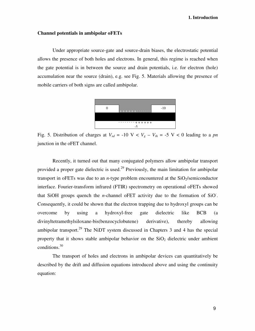
Channel potentials in ambipolar oFETs
Under appropriate source-gate and source-drain biases, the electrostatic potential
allows the presence of both holes and electrons. In general, this regime is reached when
the gate potential is in between the source and drain potentials, i.e. for electron (hole)
accumulation near the source (drain), e.g. see Fig. 5. Materials allowing the presence of
mobile carriers of both signs are called ambipolar.
0 -10
- - - - - - - -
+ + + + + +
-5 + + + + + +
- - - - - - -
Fig. 5. Distribution of charges at Vsd = -10 V < Vg – Vth = -5 V < 0 leading to a pn
junction in the oFET channel.
Recently, it turned out that many conjugated polymers allow ambipolar transport
provided a proper gate dielectric is used.29 Previously, the main limitation for ambipolar
transport in oFETs was due to an n-type problem encountered at the SiO2/semiconductor
interface. Fourier-transform infrared (FTIR) spectrometry on operational oFETs showed
that SiOH groups quench the n-channel oFET activity due to the formation of SiO-.
Consequently, it could be shown that the electron trapping due to hydroxyl groups can be
overcome by using a hydroxyl-free gate dielectric like BCB (a
divinyltetramethylsiloxane-bis(benzocyclobutene) derivative), thereby allowing
ambipolar transport.29 The NiDT system discussed in Chapters 3 and 4 has the special
property that it shows stable ambipolar behavior on the SiO2 dielectric under ambient
conditions.30
The transport of holes and electrons in ambipolar devices can quantitatively be
described by the drift and diffusion equations introduced above and using the continuity
equation:
9

RGdxdjedtdp hole −+−= − // 1
RGdxdjedtdn electron −+−= − // 1
G and R are the generation and recombination rates, respectively. At the border between
n- and p-type regions, electron and hole currents meet. A consequence of having both
carriers in close proximity is bimolecular recombination of electrons and holes. In the
bimolecular-recombination plasma, R is usually assumed to be described by a Langevin-
type equation:
npR γ= (5)
where � is the recombination prefactor. For Langevin recombination, � is given by � =
q(µel+µhole)/ε0εr. Here, q, µel and µhole are the elementary charge, and the electron and
hole mobility, respectively. Using the same approximations as for unipolar oFETs and the
current continuity equation, the ambipolar channel potential can be analytically calculated
under the assumption of a zero recombination zone width, i.e. R is infinite.11
{ } eeethsgthsgthsg VVxxVVVVxV
βββ /1
0 )(/)()( −−−−−= (6)
for 0 < x < x0
{ } hhhthsgsdthsgsdthsg VVVxLxLVVVVVxV
βββ /110 )())(()()( +−−−−+−+−= − (7)
for x0 < x < L
where x0 is the pn meeting point. The infinitely large recombination rate R leads to a
steplike increase in the potential which is, obviously, in reality not the case. Numerical
calculations are needed to take a finite R into account.
To summarize, the drift/diffusion, Poisson, and Langevin equations are the
theoretical basement to predict physical observables such as the channel potential. From
surface potential measurements by SKPM, the width of the recombination zone in light-
emitting oFETs (LEFETs) can be measured and compared to model predictions.
(4)
10

1. Introduction
Recent Monte-Carlo studies were conducted to reconsider the recombination
factor (also called rate constant) used in Langevin-type recombination. As discussed by
Groves et al.,31 deviations are reported between the exact Langevin value and measured
values for the recombination factor �. Differences amounting up to several orders of
magnitude are reported.
So far, the only physical observables that have been used to study the
recombination in LEFETs are the surface potential and the light emitted from the exciton
recombination at the p-n interface described above. LEFETs based on ambipolar single
crystals have been reported but no further studies on their recombination width are
reported. Ambipolar polymers FETs are reported to emit visible32 or infrared33,34 light.
Although optical techniques enable the direct reading of the light intensity, the lateral
accuracy is intrinsically limited by the wavelength. Moreover, in thin polymer films,
waveguiding effects by the layer may cause an apparent broadening of the recombination
zone. No optical reconstruction has been reported to deduce the real light emission
width.32,35
As discussed above, surface potential measurements are expected to give a much
higher lateral resolution. SKPM was used to measure the surface potential on an
ambipolar oFET based on NiDT.11 In Chapters 3 and 4 these results are analyzed in detail
in order to make quantitative statements about the width of the recombination zone and
the bimolecular recombination rate.
1.4 Scanning Kelvin probe microscopy
The channel potential is the potential located at the dielectric/semiconductor
interface while the surface potential is the potential on the semiconductor/vacuum
interface. In this chapter, the measurement of the surface potential V(x) by SKPM is
discussed. As mentioned above, the most convenient technique to perform non-contact
local potentiometry on organic semiconductors is SKPM. It is a non-destructive method,
easily reproducible and possibly functioning in air. The Kelvin probe aims to approach a
sharp metallic tip (probe) to a sample at distance d, as shown in Fig. 6 a).
11

�tip �sample
Evac
εtip
εsample �tip
�sample
Evac
εtip εsample
eVcpd �tip
�sample
Evac
εtip
εsample
Vcpd
d
→E
Fig. 6. Schematic of band diagrams of Kelvin probe. �tip and �sample are the work functions
of tip and sample, εtip and εsample are their respective Fermi levels, d their separating
distance. Vcpd is the contact potential difference. a) At proximity, the vacuum levels of tip
and sample are aligned. b) At closed tip-sample circuit, their Fermi level are aligned
creating a force, in order to nullify that force, the work function difference is applied in
the circuit c).
semiconductor
gate
source drain
dielectric
~ Vdc + Vac sin(ωt) Fz
� � �res
Fig. 7. Schematic of non-contact local potentiometry by SKPM. The local surface
potential is deduced by nullifying the electrostatic force Fz between tip and sample when
the condition Vcpd = Vdc is fulfilled.
At closed tip-sample circuit, see Fig. 6 b), the work function difference eVcpd
between the tip �tip and sample �sample creates a force
ddeVEeF sampletipcpd /)(/|| χχ −===→
between them that depends on the contact
a) b) c)
12
1. Introduction
potential difference Vcpd. Applying Vcpd in the circuit, as in Fig. 6 c), the force becomes
zero.
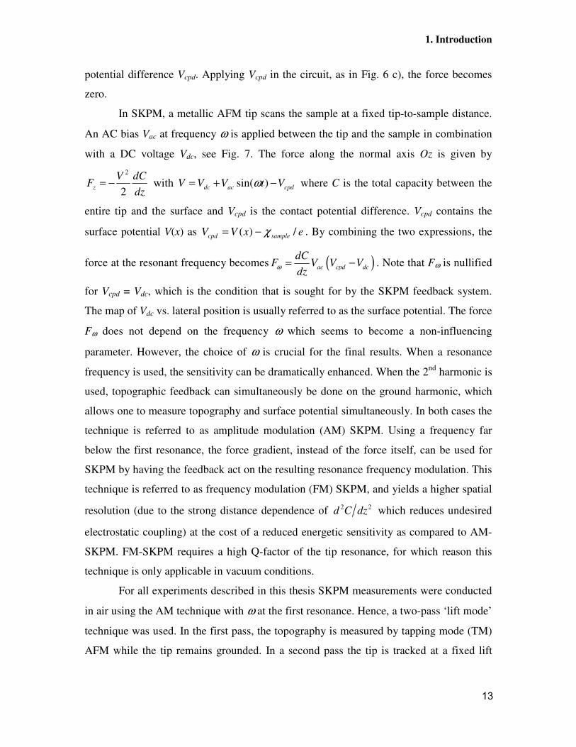
In SKPM, a metallic AFM tip scans the sample at a fixed tip-to-sample distance.
An AC bias Vac at frequency ω is applied between the tip and the sample in combination
with a DC voltage Vdc, see Fig. 7. The force along the normal axis Oz is given by 2
2z
V dCF
dz= − with cpdacdc VtVVV −+= )sin(ω where C is the total capacity between the
entire tip and the surface and Vcpd is the contact potential difference. Vcpd contains the
surface potential V(x) as exVV samplecpd /)( χ−= . By combining the two expressions, the
force at the resonant frequency becomes ( )ac cpd dc
dCF V V V
dzω = − . Note that Fω is nullified
for Vcpd = Vdc, which is the condition that is sought for by the SKPM feedback system.
The map of Vdc vs. lateral position is usually referred to as the surface potential. The force
Fω does not depend on the frequency ω which seems to become a non-influencing
parameter. However, the choice of ω is crucial for the final results. When a resonance
frequency is used, the sensitivity can be dramatically enhanced. When the 2nd harmonic is
used, topographic feedback can simultaneously be done on the ground harmonic, which
allows one to measure topography and surface potential simultaneously. In both cases the
technique is referred to as amplitude modulation (AM) SKPM. Using a frequency far
below the first resonance, the force gradient, instead of the force itself, can be used for
SKPM by having the feedback act on the resulting resonance frequency modulation. This
technique is referred to as frequency modulation (FM) SKPM, and yields a higher spatial
resolution (due to the strong distance dependence of 2 2d C dz which reduces undesired
electrostatic coupling) at the cost of a reduced energetic sensitivity as compared to AM-
SKPM. FM-SKPM requires a high Q-factor of the tip resonance, for which reason this
technique is only applicable in vacuum conditions.
For all experiments described in this thesis SKPM measurements were conducted
in air using the AM technique with ω at the first resonance. Hence, a two-pass ‘lift mode’
technique was used. In the first pass, the topography is measured by tapping mode (TM)
AFM while the tip remains grounded. In a second pass the tip is tracked at a fixed lift
13
height over the surface, using the height information obtained in the first pass. In this 2nd
pass, the surface potential is measured.
The working tip-to-surface distance, i.e. the lift height, of the SKPM affects both
resolution and sensitivity. Most AFM tips used in SKPM are made of silicon and are
metal coated. Therefore the apex radius is usually not smaller than 10 nm, causing a first
limitation to the spatial resolution at which the surface potential can be measured. Next,
the cone of the tip and the cantilever also have a capacitive coupling to the surface,
further reducing the resolution. A very small cone angle somewhat reduces the
electrostatic coupling with the surrounding area, but the final spatial resolution of AM-
SKPM is typically 100 nm or worse.
The tip-to-sample distance effect is analytically described in literature only for
systems consisting of an apex + cone.36 In this thesis, we have developed a 3D numerical
model that enables to quantitatively predict the SKPM output for any probe, i.e. including
cantilever, from a known potential distribution and geometry. The model is successfully
compared to SKPM measurements performed on relevant test devices and will be
discussed in Chapter 2.
1.5 Scanning Kelvin probe microscopy on oFETs
The previous paragraph described the surface potential mapping on metallic
surfaces. In a situation where organic layers are sandwiched between a metal electrode
and a metallic tip differences arise. On organic surfaces, the capacitive approach is still
valid although several effects complicate the interpretation of the measurements. Hudlet
et al.37 gave the force expressions of a metallic tip above metallic and semiconductor
surfaces. Fig. 8 shows the potential drop in the case of metallic (a) and semiconducting
(b) surfaces. Due to the dielectric behavior of non-degenerately doped semiconductors, a
potential drop may occur inside the semiconductor. The potential decrease inside the
semiconductor can be described by the Debye screening length 2/12 )2/( qNkTL DD ε=
where ND is the doping density, q the elementary charge, ε the permittivity, k =
1.3806.10-23 J/K the Boltzmann constant, and T the temperature. The potential drop
14

1. Introduction
reflects the bending of both valence and conduction bands, or HOMO and LUMO levels
in case of organic semiconductors.
Tip
Surface
0
QS
QM
z
0
z
V
z
V
VS
(a) (b)
LD
Fig. 8. Potential and charge distribution in the tip-surface system: (a) Metal tip/metal
surface case, (b) metal tip/semiconductor surface case, see ref. [37].
As soon as the metallic tip is above an oFET, the whole electrostatic interaction
becomes even more complex, so a number of simplifying assumptions is made:
1. The semiconductive layer above the accumulation layer is a perfect
insulator, having dielectric properties.
2. The carrier accumulation layer is located near the dielectric and is only a
few nanometers thick.
3. The metallic tip has a negligible effect on the field distribution and charge
transport in the device.
The first assumption supposes that the active layer acts as a dielectric spacer and
avoids the implementation of the Debye length LD. For instance, for ND = 1015 cm-3 in
PPV,38 the Debye length at room temperature becomes LD � 46 nm, so it is reasonable to
treat thin organic layers like a dielectric. Also other effects might cause a problem in
measured surface potentials. Let us define ltyp as the size of a feature to be discerned in
the potential trace on a polymer film of thickness d. Then, if dLD < and dltyp < the
measured surface potential is smeared out by screening and geometrical (thickness)
effects. Hence, the feature size ltyp should be larger than about 100 nm which is the case
in this thesis. The validity of the second assumption follows from the calculations in Ref.
18, where the accumulation layer is shown to be around 1 nm thick for Vsg – Vth = 10 V at
15
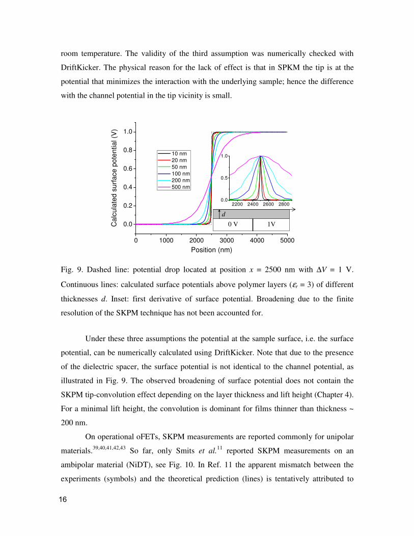
room temperature. The validity of the third assumption was numerically checked with
DriftKicker. The physical reason for the lack of effect is that in SPKM the tip is at the
potential that minimizes the interaction with the underlying sample; hence the difference
with the channel potential in the tip vicinity is small.
0 1000 2000 3000 4000 5000
0.0
0.2
0.4
0.6
0.8
1.0
0 V 1V d
2200 2400 2600 28000.0
0.5
1.0
Cal
cula
ted
surfa
ce p
oten
tial (
V)
Position (nm)
10 nm 20 nm 50 nm 100 nm 200 nm 500 nm
Fig. 9. Dashed line: potential drop located at position x = 2500 nm with ∆V = 1 V.
Continuous lines: calculated surface potentials above polymer layers (εr = 3) of different
thicknesses d. Inset: first derivative of surface potential. Broadening due to the finite
resolution of the SKPM technique has not been accounted for.
Under these three assumptions the potential at the sample surface, i.e. the surface
potential, can be numerically calculated using DriftKicker. Note that due to the presence
of the dielectric spacer, the surface potential is not identical to the channel potential, as
illustrated in Fig. 9. The observed broadening of surface potential does not contain the
SKPM tip-convolution effect depending on the layer thickness and lift height (Chapter 4).
For a minimal lift height, the convolution is dominant for films thinner than thickness ~
200 nm.
On operational oFETs, SKPM measurements are reported commonly for unipolar
materials.39,40,41,42,43 So far, only Smits et al.11 reported SKPM measurements on an
ambipolar material (NiDT), see Fig. 10. In Ref. 11 the apparent mismatch between the
experiments (symbols) and the theoretical prediction (lines) is tentatively attributed to
16
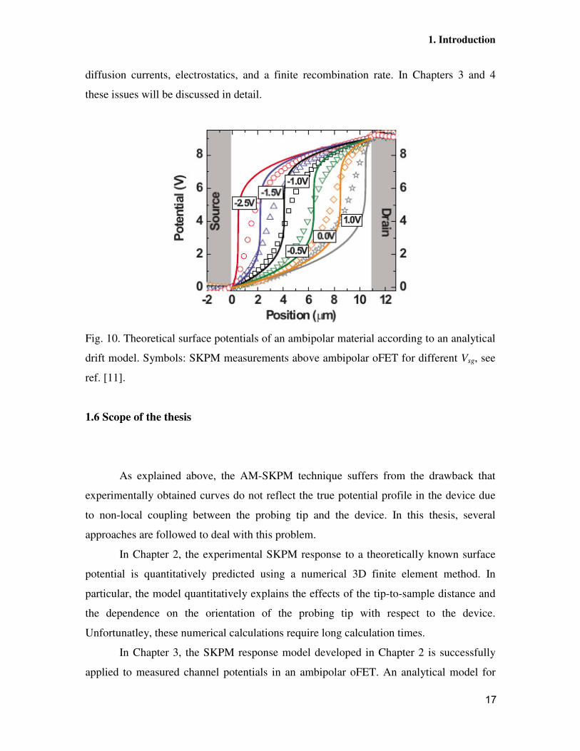
1. Introduction
diffusion currents, electrostatics, and a finite recombination rate. In Chapters 3 and 4
these issues will be discussed in detail.
Fig. 10. Theoretical surface potentials of an ambipolar material according to an analytical
drift model. Symbols: SKPM measurements above ambipolar oFET for different Vsg, see
ref. [11].
1.6 Scope of the thesis
As explained above, the AM-SKPM technique suffers from the drawback that
experimentally obtained curves do not reflect the true potential profile in the device due
to non-local coupling between the probing tip and the device. In this thesis, several
approaches are followed to deal with this problem.
In Chapter 2, the experimental SKPM response to a theoretically known surface
potential is quantitatively predicted using a numerical 3D finite element method. In
particular, the model quantitatively explains the effects of the tip-to-sample distance and
the dependence on the orientation of the probing tip with respect to the device.
Unfortunatley, these numerical calculations require long calculation times.
In Chapter 3, the SKPM response model developed in Chapter 2 is successfully
applied to measured channel potentials in an ambipolar oFET. An analytical model for
17

the recombination profile is derived and used for comparison. Assuming Langevin
recombination, the recombination zone width Wrec is found to be given by
δdWrec 34.4= with d and δ the gate dielectric and accumulation layer thicknesses,
respectively. From this analysis, we find that the actual recombination rate is two orders
of magnitude below the value predicted by the Langevin model, yielding Wrec ~ 0.5 µm.
In Chapter 4, a method based on (de)convolution with an experimentally
calibrated transfer function containing the electrostatic tip-sample coupling is developed,
which also allows reconstructing the real surface potential from a measured SKPM
response. Using this method we determined a recombination zone width of again 0.5 µm
for a NiDT ambipolar oFET. The (de)convolution methods are more flexible than the
finite element method and require negligible calculation times.
In Chapter 5, we aim at implementing a scanning-tunneling microscope-based
method, STM potentiometry (STP), to measure potentials with potentially sub-nm
resolution. In order to perform STM-potentiometry on operational oFETs in a controlled
atmosphere, a dedicated ultra high vacuum STM has been designed and built. Using
scanning tunneling spectroscopy, this instrument should also allow a direct measurement
of the density of states in the accumulation layer of an oFET. We demonstrate that it is
possible to do STM on oFETs provided that an accumulation layer of sufficient
conductivity is present in the sample, which is an important step towards STP.
Finally, in Chapter 6 we demonstrate and model a giant out-of-plane actuation
under ambient conditions in thin films of the oxidatively doped conjugated polymer blend
poly(3,4-ethylenedioxythiophene) : poly(styrenesulfonate) (PEDOT:PSS) spin cast
between interdigitated gold electrodes on glass substrates.
1.7 References and notes
[1] A. Dodabalapur, Materials Today 9, 24 (2006).
[2] E.C.P. Smits, S.G.J. Mathijssen, P.A. van Hal, S. Setayesh, T.C.T. Geuns, K.A.H.A.
Mutsaers, E. Cantatore, H.J. Wondergem, O. Werzer, R. Resel, M. Kemerink, S.
18
1. Introduction
Kirchmeyer, A.M. Muzafarov, S.A. Ponomarenko, B. de Boer, P.W.M. Blom, and D.M.
de Leeuw, Nature 455, 956 (2008).
[3] B. Comiskey, J.D. Albert, H. Yoshizawa, and J. Jacobson, Nature 394, 253 (1998).
[4] T. Sekitani, H. Nakajima, H. Maeda, T. Fukushima, T. Aida, K. Hata, and T. Someya,
Nature Mater. 8, 494 (2009).
[5] Y.Y. Deng, and H. Sirringhaus, Phys. Rev. B 72, 045207 (2005).
[6] J. Cabanillas-Gonzalez, T. Virgili, A. Gambetta, G. Lanzani, T. D. Anthopoulos, and
D.M. de Leeuw, Phys. Rev. Lett. 96, 106601 (2006).
[7] H. Tsuji, and Y. Furukawa, Mol. Cryst. Liq. Cryst. 455, 353 (2006).
[8] C. Goldmann, S. Haas, C. Krellner, K.P. Pernstich, D.J. Gundlach, and B. Batlogg, J.
Appl. Phys. 96, 2080 (2004).
[9] R. Matsubara, N. Ohashi, M. Sakai, K. Kudo, and M. Nakamura, Appl. Phys. Lett. 92,
242108 (2008).
[10] T.D. Anthopoulos, S. Setayesh, E. Smits, M. Cölle, E. Cantatore, B. de Boer,
P.W.M. Blom, and D.M. de Leeuw, Adv. Mater. 18, 1900 (2006).
[11] E.C.P. Smits, S.G.J. Mathijssen, M. Cölle, A.J.G. Mank, P.A. Bobbert, P.W.M.
Blom, B. de Boer, and D.M. de Leeuw, Phys. Rev. B 76, 125202 (2007).
[12] O.D. Jurchescu, M. Popinciuc, B.J. van Weeks, and T.T.M. Palstra, Adv. Mater. 19,
688 (2004).
[13] G. Wang, J. Swensen, D. Moses, and A.J. Heeger, J. Appl. Phys. 93, 6137 (2003).
[14] I. McCulloch, M. Heeney, C. Bailey, K. Genevicius, I. MacDonald, M. Shkunov, D.
Sparrowe, S. Tierney, R. Wagner, W. Zhang, M.L. Chabinyc, R.J. Kline, M.D. McGehee,
and M.F. Toney, Nature Mater. 5, 328 (2006).
[15] W. Geens, D. Tsamouras, J. Poortmans, and G. Hadziioannou, Synth. Met. 122, 191
(2001).
[16] H. Yan, Z. Chen, Y. Zheng, C. Newman, J.R. Quinn, F. Dötz, M. Kastler, and A.
Facchetti, Nature 457, 679 (2009).
[17] A. Tsumura, H. Koezuka, and T. Ando, Synth. Met. 25, 11 (1988).
[18] G. Horowitz, M.E. Hajlaoui, and R. Hajlaoui, J. Appl. Phys. 87, 4456 (2000).
19
[19] M.-H. Yoon, H. Yan, A. Facchetti, and T.J. Marks, J. Am. Chem. Soc. 127, 10388
(2005).�
[20] M.-H. Yoon, C. Kim, A. Facchetti, and T.J. Marks, J. Am. Chem. Soc. 128, 12851
(2006).
[21] E. Menard, V. Podzorov, S.-H. Hur, A. Gaur, M.E. Gershenson, and J.A. Rogers,
Adv. Mater. 16, 2097 (2004).
[22] H. Sirringhaus, Adv. Mater. 17, 1 (2005).
[23] Z. Bao, A. Dodabalapur, and A.J. Lovinger, Appl. Phys. Lett. 69, 4108 (1996).
[24] H. Sirringhaus, N. Tessler, and R.H. Friend, Science 280, 1741 (1998).
[25] G.H. Gelinck, T.C.T. Geuns, and D.M. de Leeuw, Appl. Phys. Lett. 77, 1487 (2000).
[26] A. Afzali, C.D. Dimitrakopoulos, and T.L. Breen, J. Am. Chem. Soc. 124, 8812
(2002).
[27] http://www.comsol.com/
[28] M.C.J.M Vissenberg, and M. Matters, Phys. Rev. B 57, 12964 (1998).
[29] L.-L. Chua, J. Zaumseil, J.-F. Chang, E.C.-W. Ou, P.K.-H. Ho, H. Sirringhaus, and
R.H. Friend, Nature 434, 194 (2005).
[30] T.D. Anthopoulos, G.C. Anyfantis, G.C. Papavassiliou, and D.M. de Leeuw, Appl.
Phys. Lett. 90, 122105 (2007).
[31] C. Groves, and N.C. Greenham, Phys. Rev. B 78, 155205 (2008).
[32] J. Zaumseil. R.H. Friend, and H. Sirringhaus, Nature Mater. 5, 69 (2006).
[33] E.C.P. Smits, S. Setayesh, T.D. Anthopoulos, M. Buechel, W. Nijssen, R. Coehoorn,
P.W.M. Blom, B. de Boer, and D.M. de Leeuw, Adv. Mater. 19, 734 (2007).
[34] L. Bürgi, M. Turbiez, R. Pfeiffer, F. Bienewald, H.-J. Kirner, C. Winnewisser, Adv.
Mater. 20, 2217 (2007).
[35] J.S. Swensen, J. Yeun, D. Gargas, S.K. Buratto, and A.J. Heeger, J. Appl. Phys. 102,
013103 (2007).
[36] C. Argento, and R.H. Friend, J. Appl. Phys. 80, 6081 (1996).
[37] S. Hudlet, M. Saint Jean, B. Roulet, J. Berger, and C. Guthmann, J. Appl. Phys. 77,
3308 (1994).
20
1. Introduction
[38] S.C. Jain, W. Geens, A. Mehra, V. Kumar, T. Aernouts, J. Poortmans, and R.
Mertens, and M. Willander, J. Appl. Phys. 89, 3804 (2001).
[39] L. Bürgi, T.J. Richards, R.H. Friend, and H. Sirringhaus, J. Appl. Phys. 94, 6129
(2003).
[40] K.P. Puntambekar, P.V. Pesavento, and C.D. Frisbie, Appl. Phys. Lett. 83, 5539
(2003).
[41] Y. Luo, F. Gustavo, J.-Y. Henry, F. Mathevet, F. Lefloch, M. Sanquer, P. Rannou,
and B. Grévin, Adv. Mater. 19, 2267 (2007).
[42] V. Palermo, M. Palma, and P. Samori, Adv. Mater. 18, 145 (2006).
[43] W.R. Silveira, and J.A. Marhon, Phys. Rev. Lett. 93, 116104 (2004).
21

22
Chapter 2
Real versus measured surface potentials in scanning Kelvin probe microscopy
2.1 Introduction
In recent years the potential mapping on organic semiconductor devices has been
steadily gaining momentum. Scanning Kelvin probe microscopy (SKPM) and electric
force microscopy (EFM) both offer unique opportunities to measure local surface
potentials with ~100 nm resolution on operational devices. Since the measured surface
potential seems to reflect the actual potential in the active layer, and this information is
otherwise unattainable, these techniques are becoming more and more popular for
characterizing physical aspects of organic thin films devices1 such as charge transport in
polymer transistors2 and charge generation in organic solar cells.3
As a consequence, the resolution of the SKPM measurements is an important
issue. Several experimental and theoretical studies have identified the tip-to-sample
distance4-14 and the tip radius15-16 as the limiting parameters. Actually, the lateral
resolution is affected by the capacitive coupling between the entire tip, including apex,
cone and lever, and the device. Due to this complex geometry, the problem is three
dimensional and so far, no predictive model has been reported in literature. The two
dimensional simulations that have been reported17-20 do not account for the asymmetric
influence of the lever,6,21 which causes the problem to become truly three dimensional.
We used a standard organic transistor layout without active layer, see Figure 1, as a
relevant test system to quantify the electrostatic tip-sample interaction. It appears that the
measured potential profile between ‘source’ and ‘drain’ electrodes strongly depends on
whether the tip is parallel or orthogonal to the channel. Moreover, only a fraction (from
23
50 % to 90 %) of the applied voltage is observed in measured potential traces. It would
seem, therefore, that further investigations are needed to quantify and understand the non-
negligible influence of the entire tip-sample interaction. This paper describes a numerical
tool, enabling the quantitative prediction of the surface potential as measured by SKPM
without the use of any fitting parameters.
The rest of this chapter is organized as follows. In the first part we will describe
the principle of the surface potential measurements which allows us to show the
experimental resolution problem in detail. In the second part we will describe the three
dimensional SKPM simulations and we will confront them with the measurements on the
test devices.
2.2 Experimental SKPM results
SKPM combines the classical Kelvin probe technique with atomic force
microscopy (AFM). Ideally, SKPM probes the electrochemical potential of the sample
under the tip apex, which in case of a metallic tip and sample with work function χtip and
χsample, respectively, is equivalent to a measurement of the contact potential difference
Vcpd = (χtip - χsample)/e , where e is the electron charge.
The SKPM measurements are performed on a commercial AFM system
(Dimension 3100 connected to a Nanoscope IIIa controller equipped with a Quadrex
module, Veeco Instruments) using metallized cantilevers (OMCL-AC240TM), Olympus,
resonant frequency –~70 kHz, spring constant ~2 N/m, lever thickness 2.8 �m, lever
length 240 �m, lever width 30 �m. The tip height is around 14 �m and the tip radius ~ 30
nm. Potential maps are taken in interleave mode in which the potential is measured at
each scan line in a second pass at a predefined lift height ∆z. An AC bias Vac at frequency
ω close to the AFM tip resonance frequency is applied between the tip and the sample, in
combination with a DC voltage Vdc. The force along the z axis is given by 2
2z
V dCF
dz= −
with cpdacdc VtVVV −+= )sin(ω where C is the entire capacity between tip and surface. By
introducing the latter expression into the force expression, the force at the resonant
24

2. Real versus measured surface potentials in scanning Kelvin probe microscopy
frequency becomes ( )ac cpd dc
dCF V V V
dzω = − . The force Fω is nullified by setting Vcpd = Vdc,
and does not depend on the resonant frequency ω which becomes a non-influencing
parameter. Strictly spoken, this is only valid for a metal/metal configuration of two
infinite plates, for the metal/semiconductor case Vcpd is different and is extensively
described by Hudlet et al.22
height (nm)
zscale = 50 nm
surface potential (V)
zscale = 10 V
Fig. 1. Top: Table showing topography and surface potential measured on a test device in
two different orientations: tip parallel to the channel and tip perpendicular to the channel.
Bottom left: schematic view of the probe area. Bottom right: Potential profile as
measured by SKPM. The symbols (lines) denote experimental data (numerical
simulations), done at 0 nm lift height. The applied potential profile is shown as dashed
line. Note the difference in potential profile depending on the cantilever orientation. The
insets show the tip and sample orientation. The blue dotted line shows a topography line
section.
2 4 6 8 10 12 14
0
2
4
6
8
10
orthogonal parallel theoretical
Position (µm)
Sur
face
pot
entia
l (V
)
0
10
20
30
40
Height (nm
)
dielectric
source
gate
drainchannel
levercone
apex
25
We performed SKPM measurements on bottom-contact, bottom gate transistor
substrates while applying a source-drain voltage of 10 V. Because of the absence of an
active layer, the naively expected potential profile is a plateau at 0 V over the source and
a plateau at 10 V over the drain, linked by a straight line in the channel, as indicated by
the dotted line in Fig. 1. The SKPM result obtained for ∆z = 0 nm is shown in Figure 1.
Wu et al 23 remarked that due to the oscillation amplitude, ∆z = 0 nm corresponds at a tip-
to-sample distance around 30 nm. Clearly, several deviations from the expected behavior
are visible. The potential profile is not constant over the electrodes, the highest curvature
does not occur at the channel edge, and the full bias of 10 V is not visible. In literature,
several reports described the same behavior.22,25-28 Moreover, depending on the tip-to-
channel orientation (orthogonal or parallel) the surface potential is dramatically different.
A second observation is the strong influence of the tip-to-sample distance, which was
discussed before4-14 as being a limiting parameter. Figure 2 shows a set of data for
different ∆z (0, 100, and 1000 nm). These observations have strong impact on the
applicability of SKPM for the investigation of (organic) transistors and other devices,
since the models to which the measured potential profiles are compared do not take these
limitations into account. It should be emphasized that even for the smallest lift height, the
error is non-negligible, as witnessed by Figs. 1 and 2. In order to overcome this problem,
the raw data are often rescaled to the expected values,29-30 although this is not common
practice.31-32 The rescaling procedure does not solve the problem for both mathematical
and practical reasons and deletes part of the information. In our case, such rescaling does
not remove the rounding in the experimental curves, nor does it repair the geometry-
induced asymmetry. In order to quantify these problems and to come to a workable link
between device model and SKPM response, we developed a fully 3D SKPM modeling.
The simulations that will be discussed in the next sections excellently fit the experimental
data, as shown by the continuous lines in Figs. 1 and 2.
26

2. Real versus measured surface potentials in scanning Kelvin probe microscopy
-2 0 2 4 6 80
3
6
90
3
6
9-2 0 2 4 6 8
Sur
face
pot
entia
l (V
)
P o s i t i o n ( µ m )
∆ z = 0 n m ∆ z = 1 0 0 n m ∆ z = 1 0 0 0 n m
Fig. 2. Experimental (symbols) and modeled (lines) surface potentials for three different
tip-surface distances ∆z over a 4.5 µm long channel. ∆z = 0 nm (squares), 100 nm
(circles) and 1000 nm (triangles). (a) With the tip orthogonal to the channel. (b) With the
tip parallel to the channel. In both cases, the measured voltage difference is decreasing
with the lift scan height. The insets show the tip and sample orientation.
2.3 Simulation of SKPM
In order to simulate the SKPM technique, we used a commercial finite-element
package which allows one to draw and subsequently simulate realistic tip and device
shapes, see Figure 3 (a) and (b). An additional organic layer, which would be present in
an actual organic field effect transistor, can be easily added in a future work. A meshing
procedure fills the entire space with tetrahedrons while conserving continuity at their
(a)
(b)
27
interfaces and builds up all object as compositions of tetrahedrons, see Fig. 3 (b). The
discrete filling of tetrahedrons causes a limitation in resolution if the meshing density is
low. The software tool used allows one to control the meshing in some detail, which is
crucial for reducing the numerical scatter to an acceptable level. The issue of numerical
noise is further addressed below in the discussion of Fig. 5. It is important to point out
that the model described above does not have any fitting parameters, i.e. all parameters
are known prior to the simulation.
Fig. 3. Three-dimensional drawing of the tip - consisting of lever, cone and apex - into a
vacuum box which determines the calculation space. The box size is 50 �m × 65 �m
(surface) × 25 �m (height). The drawn tip is not an exact replica of the tip used in the
experiments but all characteristic features (cone angle and height, apex radius, width and
tilt of the lever) are reproduced. The inset is a zoom on the tip meshing, showing that the
apex is defined as a combination of tetrahedrons which can lead to a limitation in
resolution, see text.
Subsequently the SKPM response VSKPM is calculated as follows: for a given tip-
to-sample distance and lateral tip position, the vertical force between the tip and the
surface is calculated as a function of Vdc. The force Fz versus Vdc is a parabola as expected
28
2. Real versus measured surface potentials in scanning Kelvin probe microscopy
from simple electrostatics, of which the potential VSKPM that is measured by SKPM is the
maximum, see Fig. 4.
0 1 2 3 4 5 6
-8
-6
-4
-2
0
Forc
e (n
N)
Tip voltage (V)
Fig. 4. Vertical force between the probe (including cone, apex and cantilever) and the
entire device versus bias applied to the probe. Since the SKPM technique nullifies this
force, the voltage at the extreme of the parabola equals the SKPM output VSKPM(x). The
calculation is done in the channel close to the source.
Then, for each new geometry the force between tip and surface as a function of
tip-to-sample distance is calculated. Figure 5 shows the force for both tip-to-channel
orientations. The curves are not smooth since the meshing procedure creates a slightly
different distribution of tetrahedrons after every change in geometry. However, once
proper settings are found, a relatively smooth curve with few deviating points is obtained.
In the subsequent calculation of lateral SKPM profiles the particular tip-to-sample
distances at which scatter occurs are avoided. To check if the simulated downward force
is reasonable, a comparison with analytical expressions given in literature for a system
consisting of an apex plus cone16 is made. We find that both the order of magnitude and
the behavior at small separation are similar, whereas the height dependence at larger
separation is weaker in the present case because of the (almost constant) coupling of the
relatively large lever to the sample, which is not present in the analytical expressions.
29
10 100 1000
0.1
1
10
Forc
e (n
N)
Tip-to-sample distance (nm)
Fig. 5. Vertical (downward) force between the tip and the surface versus their separating
distance. The calculations were done in the middle of channel. Empty squares (full
squares) correspond to the tip orthogonal (parallel) to the channel. The thin lines are a
guide to the eye.
Figure 2 (a) and (b) show the experimental and simulated surface potentials for
three different lift scan heights, 0 nm, 100 nm and 1000 nm, in the orthogonal and
parallel configuration. Clearly, all characteristic features in the experimental traces like
the non-constant signal above the electrodes and the loss of resolution with increasing
height are well reproduced by the calculations. Also the dependence on tip-to-channel
orientation is correctly described by the model. As anticipated, the (lack of) symmetry of
the experimental situation with respect to the middle of the channel in the (anti) parallel
situation results in (a)symmetric SKPM traces. Obviously, the real electrostatic potential
profile is symmetric in both cases. We attribute the small differences between the
experimental and modeling curves to slight differences between the modeled and true tip.
In particular, the inclination of the cantilever is known to be around 35° with errors in
fabrication. The cone height ranges between 9 and 19 µm due to fabrication margins.
Having established the model, it is worthwhile to briefly point out some ‘scaling’
properties of SKPM measurements. Figure 6 shows three different biasing configurations
that are possible with the tip orthogonal to the channel. Electrostatically, these situations
30
2. Real versus measured surface potentials in scanning Kelvin probe microscopy
are equivalent. Therefore, provided that the shape of the potential distribution V(x) is
independent of the magnitude of the bias, as is the case in our test devices, one may
anticipate that all SKPM curves can be rescaled to one ‘master curve’ that only depends
on the geometry. Obviously, the same holds for the tip parallel to the channel. For the
simulations, this result implies that per geometry only one calculation is needed and that
VSKPM(x) of configurations with different biases on the ‘source’ and ‘drain’ electrodes can
be obtained by simple rescaling. Note, however, that in many ‘real’ devices like FETs
outside the linear regime, the shape of V(x) is not independent of source-drain bias.
-2 0 2 4 6 8 10 12
-10
-8
-6
-4
-2
0
2
4
6
8
10
Vsd = 10 V Vsd =-10 V Vsd = 1 V
Position (µm)
Sur
face
pot
entia
l (V
)
0.0
0.5
1.0
Rescaled surface potential
Fig. 6. (a) Potential profiles for three different source-drain potentials Vsd = 10 V, 1 V and
-10 V (top to bottom). (b) as (a), after rescaling the curves in panel (a) by dividing them
by the applied source-drain bias.
In order to qualitatively estimate the contribution of different tip parts, Figure 7
shows the experimental potential profile in the geometry with the lever orthogonal to the
channel and three different modeling curves. The solid black line is calculated for the full
3D probe consisting of apex, cone and lever. Calculations for a probe consisting of cone
+ apex (red dashed line) and only a single apex (blue dotted line) are also shown. A few
comments can be given. As soon as the lever disappears to leave only the apex + cone,
the full potential difference at the electrodes becomes 20% higher. Moreover the non-
31
symmetric potential profile that is calculated with the full tip becomes symmetric upon
removal of the lever, reflecting the increased symmetry of the ‘reduced’ probes. When
also the cone is removed from the calculation, the potential profile becomes virtually
identical to the true surface potential. The minor deviations in the present calculation are
due to the limited number of calculated lateral points. From a comparison of these three
situations, it follows that the optimal geometry for a practical probe is one where (a) the
cone is long –to reduce the coupling between the sample and the lever– and slender –to
minimize the coupling between the sample and the cone itself and (b) the lever is narrow
–again to avoid undesired coupling to the sample. Moreover, to avoid asymmetry, the
lever is preferably kept parallel to the channel.
-2 0 2 4 6 8
0
2
4
6
8
10
Sur
face
pot
entia
l (V
)
Position (µm)
Fig. 7. Experimental potential profile in the situation with the lever orthogonal to the
channel (squares) and modeling for a full 3D tip (black line) containing the apex, cone
and lever. The red dashed line is the simulation for a probe consisting only of cone +
apex, the blue dotted line for a probe consisting of only an apex.
32
2. Real versus measured surface potentials in scanning Kelvin probe microscopy
2.4 Conclusion
Summarizing, we have shown that the potential profiles that are measured by
scanning Kelvin probe microscopy do not purely reflect the electrostatic potential under
the tip apex, but are strongly affected by the electrostatic coupling between the entire
probe and the entire device, even at small tip-sample separation. We have developed a
3D numerical model that enables one to quantitatively predict the SKPM output from a
known potential distribution and geometry. The model is successfully compared to
SKPM measurements performed on relevant test devices.
2.5 Materials and methods
The used samples were typical bottom contact and bottom gate transistor
substrates defined using UV lithography and lift-off, i.e. a device structure that is
commonly used in organic semiconductor research and technology. The structures were
fabricated on n+ - Si wafers with a thick (1 µm) thermally grown SiO2 oxide layer (εr =
3.9). The source and drain electrodes consisted of 25 nm Au on top of a 5 nm Ti adhesion
layer, and were shaped either as interdigitated fingers or as concentric rings, both with
various W/L ratios. For the present work, no substantial differences between interdigitated
and ring geometries were found.
Numerical simulations were performed using COMSOL 3.2b in combination with
MatLab 7.1 running on a desktop pc with 2 GB of internal memory. In the simulations
the entire system was split into three blocks, being the tip containing a semi-spherical
apex, a cone and a parallelepiped lever, the surrounding vacuum block and a block
representing the substrate surface and contacts (Fig. 3). Once the geometry was drawn,
the subdomain settings had to be defined, the subdomains being blocks. The tip was
defined as platinum, the space around the tip was air. An organic layer, if present, was a
dielectric layer defined with a dielectric constant εr. In order to simplify the geometry and
avoid the need of re-meshing for each lateral tip position, the electrodes were assumed to
33
have zero height, so their potential can be analytically defined via boundary condition
settings. The order of error of this assumption had not been strictly checked, since the
calculations would require a huge amount of memory which was out of our
computational possibility. However, we expected that the error was confined to a narrow
region with a width that was comparable to the electrode height, i.e. a few tens of nm. In
the modeling we assumed zero contact resistance which is the case in most devices in this
thesis. The implementation of contact resistance is possible by accordingly including the
potential steps at the electrodes.
The boundary settings were a DC potential Vdc on the tip, continuity for all the
interior boundaries and electric insulation for the exterior boundaries. The surface
potential Vcpd(x) from which the SKPM response VSKPM was to be determined was defined
as a boundary condition for the potential of the bottom surface, using an equation
function of coordinates (Oxyz). By defining the surface potential on top of the gate oxide,
the underlying bulk layers, i.e. the dielectric SiO2 and gate n+-Si, needed not to be defined
anymore since the surface potential boundary condition contained their contribution and
(by definition) screens everything underneath. Instead of moving the tip, which required
re-meshing and caused significant numerical noise, the channel was analytically moved
along the x axis. Moreover, COMSOL offered the possibility to increase locally the
meshing quality when the parameters by defaults gave a non-optimized resolution
between the apex and the surface. The ‘Maximum element size’ parameter specified the
maximum allowed element size, which by default was 1/10th of the maximum distance in
the geometry. The apex had a Maximum element size equal to 0.09 in COMSOL unit,
corresponding to 18 nm. The ‘Element growth rate’ determined the maximum rate at
which the element size can grow from a region with small elements to a region with
larger elements. The value must be greater or equal to one. In our calculation we took the
Element Growth Rate at 1.7.
2.6 References and notes
[1] S. Palermo, M. Palma, and P. Samorì, Adv. Mater. 18, 145 (2006).
34

2. Real versus measured surface potentials in scanning Kelvin probe microscopy
[2] L. Bürgi, T. Richards, M. Chiesa, R.H. Friend, and H. Sirringhaus, Synth. Met. 146,
297 (2004).
[3] D.C. Coffey, and D.S. Ginger, Nature Mater. 5, 735 (2006).
[4] Z. Weng, T. Kaminsky, G.E. Bridges, and D.J. Thomson, J. Vac. Sci. Technol. A 22,
948 (2004).
[5] G.M. Sacha, and J.J. Sáenz, Appl. Phys. Lett. 85, 2610 (2004).
[6] G. Koley, G. Spencer, and H.R. Bhangale, Appl. Phys. Lett. 79, 545 (2001).
[7] A. Gil, J. Colchero Gómez-Herrero, and A.M. Baró, Nanotechnology 14, 332 (2003).
[8] T. Takahashi, and S. Ono, Ultramicroscopy 100, 287 (2004).
[9] S. Belaidi, P. Girard, and G. Leveque, J. Appl. Phys. 81, 1023 (1997).
[10] O. Vatel, and M. Tanimoto, J. Appl. Phys. 77, 2358 (1995).
[11] R. Shikler, and Y. Rosenwaks, Appl. Surf. Sci. 157, 11041 (2000).
[12] S. Hudlet, M. Saint Jean, C. Guthmann, and J. Berger, Eur. Phys. J. B 2, 5 (1998).
[13] A.S. Foster, L.N. Kantorovich, and A.L. Shluger, Appl. Phys. A 72, 59 (2001).
[14] E. Bonaccurso, F. Schönfeld, and H.-J. Butt, Phys. Rev. B 74, 085413 (2006).
[15] G.M. Sacha, A. Verdaguer, J. Martinez, J.J. Sáenz, D.F. Ogletree, and M. Salmeron,
Appl. Phys. Lett. 86, 123101 (2005).
[16] C. Argento, and R.H. French, J. Appl. Phys. 80, 6081 (1996).
[17] E. Tevaarwerk, D.G. Keppel, P. Rugheimer, M.G. Lagally, and M.A. Eriksson, Rev.
Sci. Instrum. 76, 053707 (2005).
[18] H.O. Jacobs, P. Leuchtmann, O.J. Homan, and A. Stemmer, J. Appl. Phys. 84, 1168
(1998).
[19] T.S. Gross, C.M. Prindle, K. Chamberlin, N. bin Kamsah, and Y. Wu,
Ultramicroscopy 87, 147 (2001).
[20] S. Belaidi, F. Lebon, P. Girard, G. Leveque, and S. Pagano, Appl. Phys. A 66, 239
(1998).
[21] T. Hochwitz, A.K. Henning, C. Levey, C. Daghlian, and J. Slinkman, J. Vac. Sci.
Technol. B 14, 457 (1996).
[22] S. Hudlet, M. Saint Jean, B. Roulet, J. Berger, and C. Guthmann, J. Appl. Phys. 77,
3308 (1995).
[23] Y. Wu, and M.A. Shannon, Rev. Sci. Instrum. 77, 043711 (2006).
35
[24] J.A. Nichols, D.J. Gundlach, and T.N. Jackson, Appl. Phys. Lett. 83, 2366 (2003).
[25] K. Müller, A. Goryachko, Y. Burkov, C. Schwiertz, M. Ratzke, J. Köble, J. Reif, and
D. Schmeißer, Synth. Met. 146, 377 (2004).
[26] C.H. Lei, A. Das, M. Elliot, and J.E. Macdonald, Nanotechnology 15, 627 (2004).
[27] U. Zerweck, C. Loppacher, T. Otto, S. Grafström, and L.M. Eng, Phys. Rev B 71,
125424 (2005).
[28] Y. Luo, F. Gustavo, J.-Y. Henry, F. Mathevet, F. Lefloch, M. Sanquer, P. Rannou,
and B. Grévin, Adv. Mater. 19, 2267 (2007).
[29] K.P. Puntambekar, P.V. Pesavento, and C.D. Frisbie, Appl. Phys. Lett. 83, 5539
(2003).
[30] E.C.P. Smits, S.G.J. Mathijssen, M. Cölle, A.J.G. Mank, P.A. Bobbert, P.W.M.
Blom, B. de Boer, and D.M. de Leeuw, Phys. Rev B 76, 125202 (2007).
[31] W.R. Silveira, and J.A. Marohn, Phys. Rev. Lett. 93, 116104 (2004).
[32] L. Bürgi, H. Sirringhaus, and R.H. Friend, Appl. Phys. Lett. 80, 2913 (2002).
36

Chapter 3
On the width of the recombination zone in organic light emitting field effect transistors
3.1 Introduction
The recent realization of bipolar currents in organic field effect transistors has
enabled the fabrication of organic light emitting field effect transistors (LEFET).1 The
high current densities in these devices2 as compared to those in diode-type devices may
help to reach population inversion which is a prerequisite for an electrically driven
organic laser.3 Apart from the possible use in an organic lasing device, LEFET may offer
significant advantages over conventional organic light emitting diodes (OLED). Not only
the high current density, but also the possibility to shift the recombination zone away
from the metallic contacts and the fact that all free carriers contribute to exciton
formation can lead to increased brightness and efficiency.1,4 However, the high carrier
and exciton densities in LEFET may also enhance exciton quenching, reducing the
internal quantum efficiency.2,4,5
Since exciton-exciton and exciton-carrier quenching rates are strong functions of
the exciton and carrier density, both the maximum attainable exciton density and the in-
and external quantum efficiency of LEFET strongly depend on the width of the
recombination zone. So far, the actual value of the recombination zone width W has
received surprisingly little attention. In theoretical works, W is commonly taken to be
zero, i.e. an infinite bimolecular recombination rate R is assumed.6,7,8 Experimentally,
both confocal optical9 and electrostatical10 methods have been employed to resolve the
37
recombination profile, yielding values for W in the micrometer range. However, both
techniques suffer from a non-negligible finite spatial resolution.
Here, we present an analytical model for the width and shape of the
recombination profile in ambipolar transistors, including LEFET.11 The results compare
favorably to numerical calculations and indicate that W ≈ 100 nm for typical organic
LEFET when R is taken equal to the Langevin rate. This observation is supported by a
detailed analysis of surface potential profiles as measured by scanning Kelvin probe
microscopy (SKPM).
3.2 Analytical model of recombination width
With the analytical model, one allows to calculate the recombination of electrons
and holes in the recombination zone of a LEFET. For this, we divide the device in three
regions as illustrated in Fig. 1. In the regions between the source and drain contacts and
the recombination zone we apply the gradual channel approximation12, i.e. the hole and
electron densities are given by ( )( ) gp C V x V= − and ( )( )gn C V V x= − , with V(x) and Vg
the (local) channel and gate potential, respectively. 0 rC dε ε= is the gate capacitance
with εr and d the relative dielectric constant and thickness of the gate insulator. Inside the
recombination zone we assume that the carrier densities are determined by the
recombination process only. Assuming further a constant electrostatic field F, the hole
and electron drift current densities are h hj qp Fµ= and e ej qp Fµ= with q the
elementary charge, p, n the hole and electron density and µh, µe the hole and electron
mobility, respectively. Using a Langevin-type recombination rate R npγ= one finds for
the hole and electron density
h e
dp dp dx dp dn dnv np v
dt dx dt dx dx dtγ= = = − = = (1)
where h hv Fµ= and e ev Fµ= − are the hole and electron drift velocities. In (1)
diffusion effects are tacitly ignored, which will be justified below.
38

3. On the width of the recombination zone in organic light emitting field effect transistors
gatedielectric
source drainsemiconductor
x
eVn,
p, R
Vs
Vd
Vg∆Vsd
V(x)
pn
n’p’
W
R
gatedielectric
source drainsemiconductor
x
eVn,
p, R
Vs
Vd
Vg∆Vsd
V(x)
pn
n’p’
W
R
Fig.1. Schematic layout of the LEFET as assumed in the analytical model. The top panel
shows carrier densities and recombination vs. position in the LEFET channel. The middle
panel shows the potential profile and the bottom panel the device layout. Parameters are
explained in the text. Note that n’, p’ are symmetric, whereas n, p are not.
Defining effective densities ' hp pµ≡ and ' hn nµ≡ current conservation demands
that the limiting values of p′ , n′ on either side of the recombination zone are equal, i.e.
0 0p n j qF′ ′= = . For a given source-drain voltage Vsd, this condition fixes the gate
voltage to )/1/( ehsdgssg VVVV µµ+=−=− , to be used later. Moreover, one has
0 0( ) ( )p x n x p n′ ′ ′ ′+ = = everywhere in the recombination zone. With these definitions one
easily arrives at the following differential equations
( ) ( )0 0 and dp dn
p p p n n ndx dx
α α′ ′′ ′ ′ ′ ′ ′= − − = − (2)
39
with h eFα γ µ µ≡ . Taking the source (drain) on the left (right) and for the source (Vs),
gate (Vg) and drain (Vd) voltages s g dV V V> > as in Fig. 1, the solution of (2) is
( )
( )( )
0 0 00
0 0 0 0
exp and
exp 1 exp 1
n n x xpp n
p x x n x x
αα α
′ ′ −� �′ � �′ ′= =′ ′− + − +� � � �� � � �
(3)
with x0 the position of the center of the recombination zone where 10 0 02( ) ( )p x n x n′ ′ ′= = .
The recombination profile follows from R npγ= , i.e.
( )
( )( )2
0 002
0 0
exp
exp 1h e
n x xnR
n x x
αγµ µ α
′ +� �′ � �=′ + +� �� �
. (4)
Taking W as the width at which R reaches 1/e of its maximum value, one obtains
04.34W n α′= .
In order to apply the above to actual devices, estimates for the boundary
conditions 0p′ , 0n′ and the field F need to be made. Defining ∆Vsd as the voltage drop
over the recombination zone one finds from their definitions that α ~ sdVWF ∆= //1 and
0n′ ~ sdV∆ . Hence 04.34W n α′= becomes the square root of a constant, i.e. independent
of ∆Vsd. The full expression for W is easiest obtained by setting ∆Vsd = Vsd, i.e.
sdF V W= . The gate bias determines p0 according to ( )00
rs gp V V
qdε ε
δ= − with δ the
thickness of the accumulation layer. Using ( )1s g sd h eV V V µ µ− = + as derived above
from current conservation, and the Langevin13 value for the recombination prefactor
( ) 0h e rqγ µ µ ε ε= + one finally finds
4.34W dδ= (5)
Typical values for δ are around 1–10 nm,14 and for d 50 nm – 1 µm, giving W
values in the range 15 – 200 nm. The surprisingly few parameters in (5) reflect the
cancellation of (a) the mobility dependence of the drift velocity and recombination rate,
40

3. On the width of the recombination zone in organic light emitting field effect transistors
(b) the dielectric constant dependence of the capacitance and recombination rate and (c)
the bias dependence of the carrier density (~Vg) and drift velocity (~Vsd) since Vg and Vsd
are linked by current conservation as discussed above.
Let us now briefly come back to the ignored effects of carrier diffusion. The
broadening of the recombination profile due to diffusion can be estimated from
diffW Dτ≈ . Here, D is the diffusion constant, linked to the mobility via the Einstein
relation BD k T qµ= with kB the Boltzmann constant and T the absolute temperature. The
recombination time constant τ is estimated as 01 nτ γ≈ . With this, the diffusion
broadening becomes diff B sdW W k T qV≈ . Since the square root term is much smaller
than unity for all practical devices as Bk T q ≈ 25 meV at room temperature, the diffusion
broadening can indeed safely be ignored.
In Fig. 2, the predictions of Eqs. 3-5 are compared to numerical solutions of the
coupled drift/diffusion and Poisson equations. The parameters used correspond to the
nickel dithiolene (NiDT) devices described in Ref. 10. Clearly, both the height and shape
of the recombination profile, and correspondingly the decay of the electron and hole
density, are accurately reproduced by the analytical model. In the bottom panel of Fig. 2
the numerically and analytically calculated recombination profiles for three different
accumulation layer thicknesses are compared. Indeed, the numerically obtained profile
has a width that follows Eq. 5. It should be pointed out that the numerically calculated
recombination profile is extremely sensitive to undersampling, i.e. a too coarse
calculation grid will result in overestimation of W, usually without much effect on the
calculated current densities. Likely, this explains the large differences between the
present results and those in Ref. 15. Our calculated widths do match well with those
found by Smith and Ruden.16
41
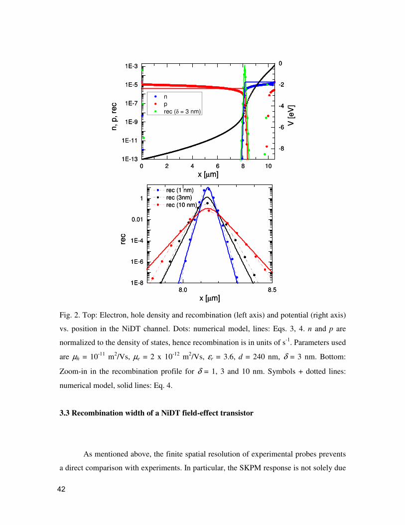
0 2 4 6 8 101E-13
1E-11
1E-9
1E-7
1E-5
1E-3
-8
-6
-4
-2
0
n, p
, rec
x [µm]
n p rec (δ = 3 nm)
V [e
V]
8.0 8.51E-8
1E-6
1E-4
0.01
1
rec (1 nm) rec (3nm) rec (10 nm)
rec
x [µm]
0 2 4 6 8 101E-13
1E-11
1E-9
1E-7
1E-5
1E-3
-8
-6
-4
-2
0
n, p
, rec
x [µm]
n p rec (δ = 3 nm)
V [e
V]
8.0 8.51E-8
1E-6
1E-4
0.01
1
rec (1 nm) rec (3nm) rec (10 nm)
rec
x [µm]
Fig. 2. Top: Electron, hole density and recombination (left axis) and potential (right axis)
vs. position in the NiDT channel. Dots: numerical model, lines: Eqs. 3, 4. n and p are
normalized to the density of states, hence recombination is in units of s-1. Parameters used
are µh = 10-11 m2/Vs, µe = 2 x 10-12 m2/Vs, εr = 3.6, d = 240 nm, δ = 3 nm. Bottom:
Zoom-in in the recombination profile for δ = 1, 3 and 10 nm. Symbols + dotted lines:
numerical model, solid lines: Eq. 4.
3.3 Recombination width of a NiDT field-effect transistor
As mentioned above, the finite spatial resolution of experimental probes prevents
a direct comparison with experiments. In particular, the SKPM response is not solely due
42
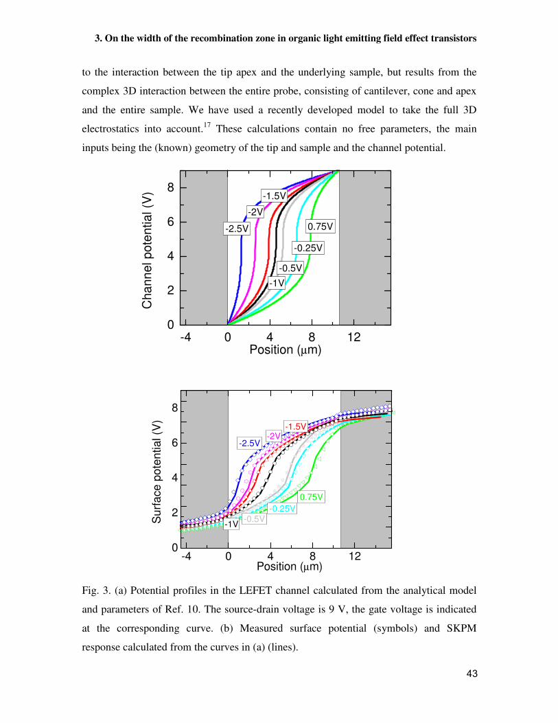
3. On the width of the recombination zone in organic light emitting field effect transistors
to the interaction between the tip apex and the underlying sample, but results from the
complex 3D interaction between the entire probe, consisting of cantilever, cone and apex
and the entire sample. We have used a recently developed model to take the full 3D
electrostatics into account.17 These calculations contain no free parameters, the main
inputs being the (known) geometry of the tip and sample and the channel potential.
-4 0 4 8 120
2
4
6
8
Cha
nnel
pot
entia
l (V
)
Position (µm)
-1V
-2.5V
-2V0.75V
-0.25V
-1.5V
-0.5V
-4 0 4 8 120
2
4
6
8
-1V
-2.5V-2V
Sur
face
pot
entia
l (V
)
Position (µm)
0.75V-0.25V
-1.5V
-0.5V
Fig. 3. (a) Potential profiles in the LEFET channel calculated from the analytical model
and parameters of Ref. 10. The source-drain voltage is 9 V, the gate voltage is indicated
at the corresponding curve. (b) Measured surface potential (symbols) and SKPM
response calculated from the curves in (a) (lines).
43

As input for the channel potential we use the analytical expressions for V(x) as
derived by Smits et al., see Fig. 3a.10 These calculations are based on variable range
hopping in an exponential density of states, and assume W = 0. The calculation of the
surface potential takes only parameters as inputs that are independently determined, i.e.
the entire calculation is free of fitting parameters. The calculated surface potentials
accurately match the measured ones, as shown in Fig. 3b. Within their error margins, the
shapes of the experimental and numerical traces are equal. A detailed analysis of the
calculated and measured surface potentials in the recombination region allows us to put
an upper limit to the width of the actual recombination zone of less than 0.5 µm.
In order to arrive at values for W that are in the µm range, as claimed by Swensen et
al. on basis of confocal microscopy experiments9, the recombination prefactor needs to
be set significantly below the Langevin value that is used in this paper. Reducing γ by a
factor β (β < 1) leads to an increase in W by a factor β-1/2.
3.4 Conclusion
Summarizing, we have presented an analytical model for the recombination
profile in organic ambipolar FETs. The model only depends on experimentally easily
accessible parameters and predicts a recombination zone width in the range 15 – 200 nm,
which is confirmed by numerical calculations. A detailed analysis of the surface potential
obtained by scanning Kelvin probe microscopy on nickel dithiolene LEFET supports the
notion of a narrow recombination zone.
3.5 References and notes
[1] For a recent review see e.g. J. Zaumseil, and H. Sirringhaus, Chem. Rev. 107, 1296
(2007).
44

3. On the width of the recombination zone in organic light emitting field effect transistors
[2] T. Takenobu, S.Z. Bisri, T. Takahashi, M. Yahiro, C. Adachi, and Y. Iwasa, Phys.
Rev. Lett. 100, 066601 (2008).
[3] For a recent review see e.g. I.D.W. Samuel, and G. A. Turnbull, Chem. Rev. 107,
1272 (2007).
[4] J. Zaumseil, R.H. Friend and H. Sirringhaus, Nature Mater. 5, 69 (2006).
[5] S. Verlaak, D. Cheyns, M. Debucquoy, V. Arkhipov, and P. Heremans, Appl. Phys.
Lett. 85, 2405 (2004).
[6] D.L. Smith and P.P. Ruden, Appl. Phys. Lett. 89, 233519 (2006).
[7] E.C.P. Smits, T.D. Anthopoulos, S. Setayesh, E. van Veenendaal, R. Coehoorn,
P.W.M. Blom, B. de Boer, and D.M. de Leeuw, Phys. Rev. B 73, 205316 (2006).
[8] R. Schmechel, M. Ahles and H. von Seggern, J. Appl. Phys. 98, 084511 (2005).
[9] J.S. Swensen, J. Yuen, D. Gargas, S.K. Buratto, and A.J. Heeger, J. Appl. Phys. 102,
013103 (2007).
[10] E.C.P. Smits, S.G.J. Mathijssen, M. Cölle, A.J.G. Mank, P.A. Bobbert, P.W.M.
Blom, B. de Boer, and D.M. de Leeuw, Phys. Rev. B 76, 125202 (2007).
[11] For this problem, only the capture rate of positive and negative charges matters, the
question whether subsequent recombination is emissive or not is irrelevant. Hence the
model is valid for any ambipolar field effect transistor.
[12] S.M. Sze, Physics of Semiconductor Devices, 2nd edition, Wiley, New York, 1981.
[13] P. Langevin, Ann. Chim. Phys., serie 7, 433 (1903).
[14] G. Horowitz, R. Hajlaoui and P. Delannoy, J. de Physique III 5, 355 (1995).
[15] G. Paasch, T. Lindner, C. Rost-Bietsch, S. Karg, W. Riess, and S. Scheinert, J. Appl.
Phys. 98, 084505 (2005).
[16] D.L. Smith, and P. P. Ruden, J. Appl. Phys. 101, 084503 (2007).
[17] D.S.H. Charrier, M. Kemerink, B.E. Smalbrugge, T. de Vries, and R.A.J. Janssen,
ACS Nano 2, 622 (2008).
45

46

Chapter 4
Bimolecular recombination in ambipolar organic field effect transistors
4.1 Introduction
At present, there is significant debate on the strength of bimolecular
recombination in organic semiconducting materials.1 Not only does this issue relate to our
understanding of fundamental processes in a large class of disordered materials, but it
also translates directly into device performance. A device type in which the bimolecular
recombination strength is of great relevance is the recently developed organic light
emitting field effect transistor (LEFET).2 The high current densities in these devices3 as
compared to those in diode-type devices may help to reach population inversion, which is
a prerequisite for an electrically driven organic laser,45
-6 and may offer significant
advantages for lighting applications. However, the high carrier and exciton densities in
LEFET may also enhance exciton quenching, reducing the internal quantum efficiency.3,7
As such, knowledge of the actual exciton density is crucial. The latter is directly related
to the width of the recombination zone W, which in turn, is governed by the bimolecular
recombination strength �. In the previous chapter we have shown that W is given by8
4.34W dδ β= (1)
with d and � the thickness of the gate dielectric and the accumulation layer, respectively.
The parameter � is defined as Lγ βγ= with �L the Langevin recombination strength.
Reported values for � vary from around unity to orders of magnitude below unity.1
47
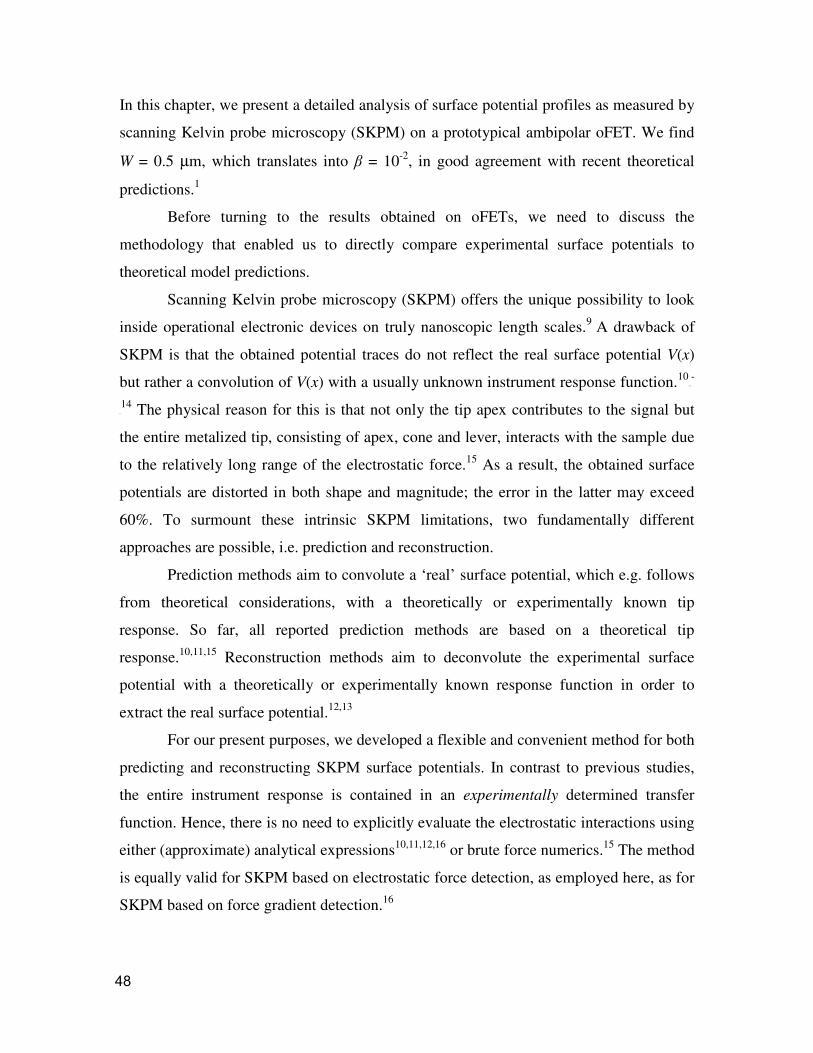
In this chapter, we present a detailed analysis of surface potential profiles as measured by
scanning Kelvin probe microscopy (SKPM) on a prototypical ambipolar oFET. We find
W = 0.5 µm, which translates into � = 10-2, in good agreement with recent theoretical
predictions.1
Before turning to the results obtained on oFETs, we need to discuss the
methodology that enabled us to directly compare experimental surface potentials to
theoretical model predictions.
Scanning Kelvin probe microscopy (SKPM) offers the unique possibility to look
inside operational electronic devices on truly nanoscopic length scales.9 A drawback of
SKPM is that the obtained potential traces do not reflect the real surface potential V(x)
but rather a convolution of V(x) with a usually unknown instrument response function.101112
-
13
14 The physical reason for this is that not only the tip apex contributes to the signal but
the entire metalized tip, consisting of apex, cone and lever, interacts with the sample due
to the relatively long range of the electrostatic force.15 As a result, the obtained surface
potentials are distorted in both shape and magnitude; the error in the latter may exceed
60%. To surmount these intrinsic SKPM limitations, two fundamentally different
approaches are possible, i.e. prediction and reconstruction.
Prediction methods aim to convolute a ‘real’ surface potential, which e.g. follows
from theoretical considerations, with a theoretically or experimentally known tip
response. So far, all reported prediction methods are based on a theoretical tip
response.10,11,15 Reconstruction methods aim to deconvolute the experimental surface
potential with a theoretically or experimentally known response function in order to
extract the real surface potential.12,13
For our present purposes, we developed a flexible and convenient method for both
predicting and reconstructing SKPM surface potentials. In contrast to previous studies,
the entire instrument response is contained in an experimentally determined transfer
function. Hence, there is no need to explicitly evaluate the electrostatic interactions using
either (approximate) analytical expressions10,11,12,16 or brute force numerics.15 The method
is equally valid for SKPM based on electrostatic force detection, as employed here, as for
SKPM based on force gradient detection.16
48
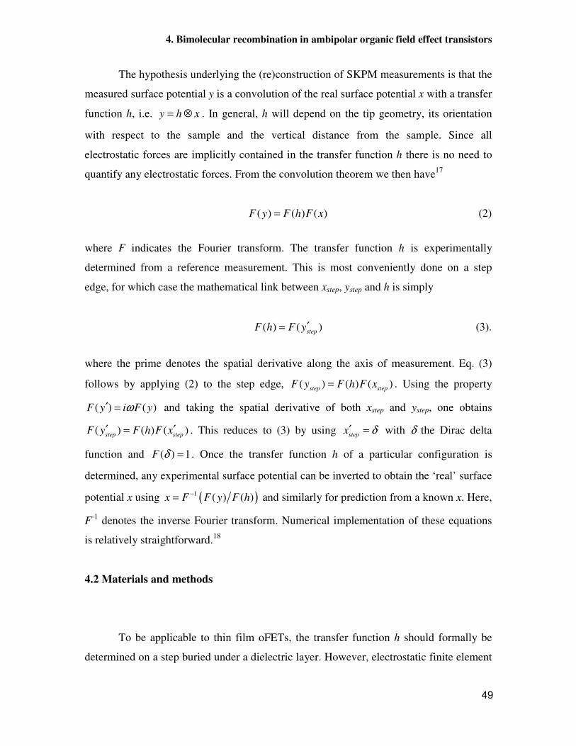
4. Bimolecular recombination in ambipolar organic field effect transistors
The hypothesis underlying the (re)construction of SKPM measurements is that the
measured surface potential y is a convolution of the real surface potential x with a transfer
function h, i.e. y h x= ⊗ . In general, h will depend on the tip geometry, its orientation
with respect to the sample and the vertical distance from the sample. Since all
electrostatic forces are implicitly contained in the transfer function h there is no need to
quantify any electrostatic forces. From the convolution theorem we then have17
( ) ( ) ( )F y F h F x= (2)
where F indicates the Fourier transform. The transfer function h is experimentally
determined from a reference measurement. This is most conveniently done on a step
edge, for which case the mathematical link between xstep, ystep and h is simply
( ) ( )stepF h F y′= (3).
where the prime denotes the spatial derivative along the axis of measurement. Eq. (3)
follows by applying (2) to the step edge, ( ) ( ) ( )step stepF y F h F x= . Using the property
( ) ( )F y i F yω′ = and taking the spatial derivative of both xstep and ystep, one obtains
( ) ( ) ( )step stepF y F h F x′ ′= . This reduces to (3) by using stepx δ′ = with δ the Dirac delta
function and ( ) 1F δ = . Once the transfer function h of a particular configuration is
determined, any experimental surface potential can be inverted to obtain the ‘real’ surface
potential x using ( )1 ( ) ( )x F F y F h−= and similarly for prediction from a known x. Here,
F-1 denotes the inverse Fourier transform. Numerical implementation of these equations
is relatively straightforward.18
4.2 Materials and methods
To be applicable to thin film oFETs, the transfer function h should formally be
determined on a step buried under a dielectric layer. However, electrostatic finite element
49
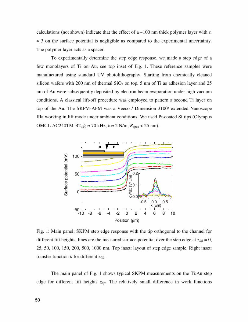
calculations (not shown) indicate that the effect of a ~100 nm thick polymer layer with �r
≈ 3 on the surface potential is negligible as compared to the experimental uncertainty.
The polymer layer acts as a spacer.
To experimentally determine the step edge response, we made a step edge of a
few monolayers of Ti on Au, see top inset of Fig. 1. These reference samples were
manufactured using standard UV photolithography. Starting from chemically cleaned
silicon wafers with 200 nm of thermal SiO2 on top, 5 nm of Ti as adhesion layer and 25
nm of Au were subsequently deposited by electron beam evaporation under high vacuum
conditions. A classical lift-off procedure was employed to pattern a second Ti layer on
top of the Au. The SKPM-AFM was a Veeco / Dimension 3100/ extended Nanoscope
IIIa working in lift mode under ambient conditions. We used Pt-coated Si tips (Olympus
OMCL-AC240TM-B2, f0 ≈ 70 kHz, k ≈ 2 N/m, Rapex < 25 nm).
-10 -8 -6 -4 -2 0 2 4 6 8 10-50
0
50
100
-0.5 0.0 0.50.0
0.1
0.2
dV
/dx
(V/µ
m)
x (µm)
Sur
face
pot
entia
l (m
V)
Position (µm)
Fig. 1: Main panel: SKPM step edge response with the tip orthogonal to the channel for
different lift heights, lines are the measured surface potential over the step edge at zlift = 0,
25, 50, 100, 150, 200, 500, 1000 nm. Top inset: layout of step edge sample. Right inset:
transfer function h for different zlift.
The main panel of Fig. 1 shows typical SKPM measurements on the Ti:Au step
edge for different lift heights zlift. The relatively small difference in work functions
50
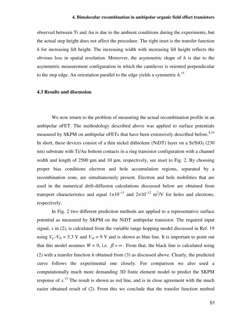
4. Bimolecular recombination in ambipolar organic field effect transistors
observed between Ti and Au is due to the ambient conditions during the experiments, but
the actual step height does not affect the procedure. The right inset is the transfer function
h for increasing lift height. The increasing width with increasing lift height reflects the
obvious loss in spatial resolution. Moreover, the asymmetric shape of h is due to the
asymmetric measurement configuration in which the cantilever is oriented perpendicular
to the step edge. An orientation parallel to the edge yields a symmetric h.15
4.3 Results and discussion
We now return to the problem of measuring the actual recombination profile in an
ambipolar oFET. The methodology described above was applied to surface potentials
measured by SKPM on ambipolar oFETs that have been extensively described before.8,19
In short, these devices consist of a thin nickel dithiolene (NiDT) layer on a Si/SiO2 (230
nm) substrate with Ti/Au bottom contacts in a ring transistor configuration with a channel
width and length of 2500 µm and 10 µm, respectively, see inset to Fig. 2. By choosing
proper bias conditions electron and hole accumulation regions, separated by a
recombination zone, are simultaneously present. Electron and hole mobilities that are
used in the numerical drift-diffusion calculations discussed below are obtained from
transport characteristics and equal 1×10⁻¹¹ and 2×10⁻¹² m2/V for holes and electrons,
respectively.
In Fig. 2 two different prediction methods are applied to a representative surface
potential as measured by SKPM on the NiDT ambipolar transistor. The required input
signal, x in (2), is calculated from the variable range hopping model discussed in Ref. 19
using Vg–Vth = 5.3 V and Vsd = 9 V and is shown as blue line. It is important to point out
that this model assumes W = 0, i.e. β = ∞ . From that, the black line is calculated using
(2) with a transfer function h obtained from (3) as discussed above. Clearly, the predicted
curve follows the experimental one closely. For comparison we also used a
computationally much more demanding 3D finite element model to predict the SKPM
response of x.15 The result is shown as red line, and is in close agreement with the much
easier obtained result of (2). From this we conclude that the transfer function method
51
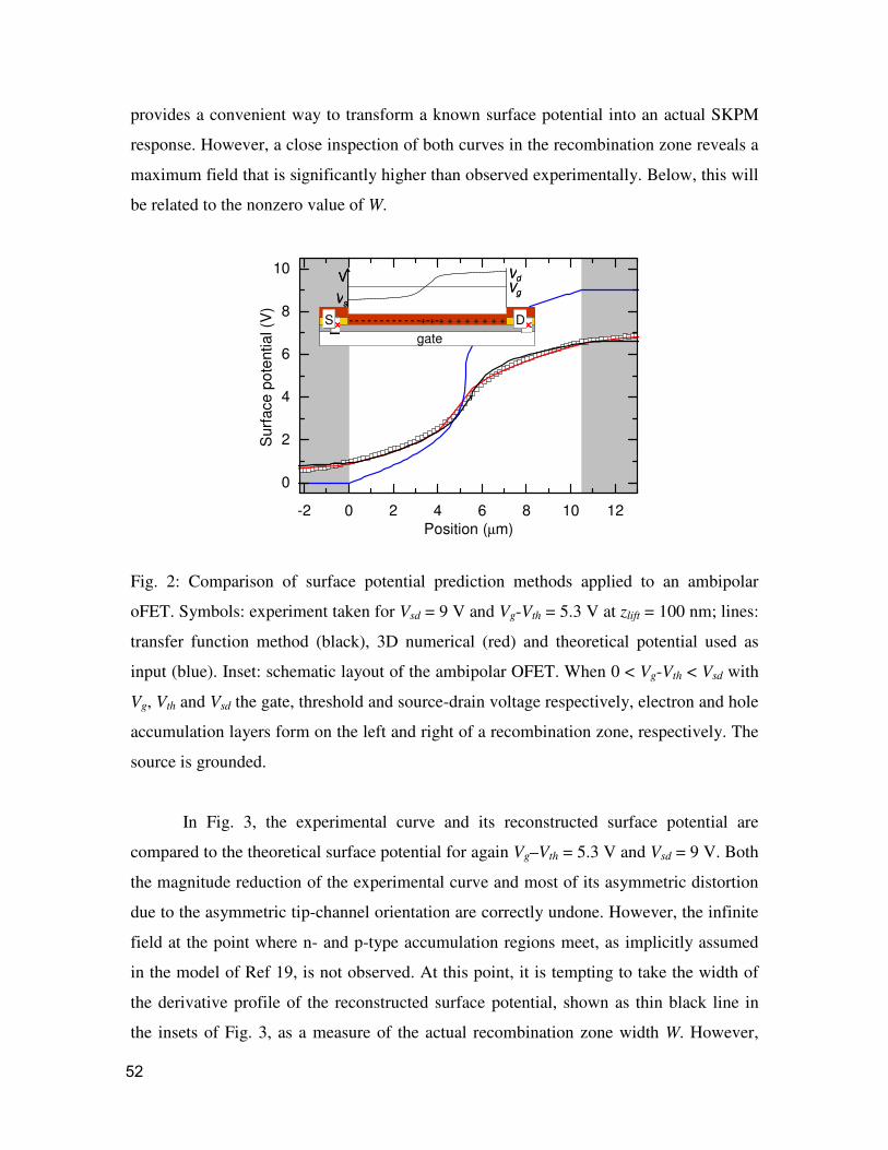
provides a convenient way to transform a known surface potential into an actual SKPM
response. However, a close inspection of both curves in the recombination zone reveals a
maximum field that is significantly higher than observed experimentally. Below, this will
be related to the nonzero value of W.
-2 0 2 4 6 8 10 12
0
2
4
6
8
10
Position (µm)
Sur
face
pot
entia
l (V
)
Fig. 2: Comparison of surface potential prediction methods applied to an ambipolar
oFET. Symbols: experiment taken for Vsd = 9 V and Vg-Vth = 5.3 V at zlift = 100 nm; lines:
transfer function method (black), 3D numerical (red) and theoretical potential used as
input (blue). Inset: schematic layout of the ambipolar OFET. When 0 < Vg-Vth < Vsd with
Vg, Vth and Vsd the gate, threshold and source-drain voltage respectively, electron and hole
accumulation layers form on the left and right of a recombination zone, respectively. The
source is grounded.
In Fig. 3, the experimental curve and its reconstructed surface potential are
compared to the theoretical surface potential for again Vg–Vth = 5.3 V and Vsd = 9 V. Both
the magnitude reduction of the experimental curve and most of its asymmetric distortion
due to the asymmetric tip-channel orientation are correctly undone. However, the infinite
field at the point where n- and p-type accumulation regions meet, as implicitly assumed
in the model of Ref 19, is not observed. At this point, it is tempting to take the width of
the derivative profile of the reconstructed surface potential, shown as thin black line in
the insets of Fig. 3, as a measure of the actual recombination zone width W. However,
V Vg Vs
Vd
gat - - - - - - - - - - - - + - + - + + + + + + + + S D
V V g Vs
Vd
gate - - - - - - - - - - - - + - + - + + + + + + + + S D
52
4. Bimolecular recombination in ambipolar organic field effect transistors
despite the fact that the analytical model underlying (1) correctly predicts the
recombination profile, it makes no predictions of the corresponding potential profile, and
the widths of the two profiles are usually not equal.8 Hence we performed a numerical
drift-diffusion analysis as outlined in Ref. 8, and compared the (spatial derivative of the)
resulting potential profiles to the reconstructed experimental profile, as shown in the
lower inset of Fig. 3. We find optimal agreement between the two derivative profiles
when parameters that give rise to a recombination zone width of 0.5 µm are used. With d
= 200 nm and estimating � = 3 nm, it follows from (1) that 210β −≈ , which is also used
in the numerical calculations.
-2 0 2 4 6 8 10 12
0
2
4
6
8
10
Position (µm)
Sur
face
pot
entia
l (V
)
2 4 6 8
dV
/dx
(nor
mal
ized
)
0 5 10 dV
/dx
(nor
mal
ized
)
Fig. 3: Reconstruction of the surface potential of an ambipolar oFET. Symbols:
experiment taken for Vsd = 9 V and Vg-Vth = 5.3 V at zlift = 100 nm; lines: transfer function
method (black) and theoretical potential as calculated according to Ref. 19 (blue). Upper
inset: normalized first derivative of the curves in the main panel. Lower inset: zoom-in on
reconstructed first derivative profile (black) and calculated profile for a recombination
zone width of 0.5 µm (red).
This implies that the bimolecular recombination rate is two orders of magnitude
below the value predicted by the Langevin expression. This finding is in good agreement
53
with the results from Monte Carlo simulations by Groves and Greenham,1 who find
values for � between 10-1 and 10-2 for similar parameters as in the present experiment.
Indeed, they showed that by shrinking the dimensionality from 3D (bulk) to 2D (planar
device as LEFET) � also decreases, and this is checked for different carrier densities. �
decreases while the effective intercarrier spacing for a given charge density increases as
transport in one dimension is increasingly constrained.
4.4 Conclusion
Summarizing, we presented a practical method for prediction and reconstruction
of surface potentials measured by SKPM. The method is based on (de)convolution with a
transfer function containing the whole electrostatic tip-sample coupling. The transfer
function is experimentally calibrated on an ‘ideal’ step edge. Using this method we
determined a recombination zone width of 0.5 µm for a NiDT ambipolar oFET,
indicating a bimolecular recombination rate that is two orders of magnitude below the
Langevin value.
4.5 References and notes
[1] See e.g. C. Groves, and N.C. Greenham, Phys. Rev. B 78, 155205 (2008) and
references therein.
[2] For a recent review see e.g. J. Zaumseil, and H. Sirringhaus, Chem. Rev. 107, 1296
(2007).
[3] T. Takenobu, S.Z. Bisri, T. Takahashi, M. Yahiro, C. Adachi, and Y. Iwasa, Phys.
Rev. Lett. 100, 066601 (2008).
[4] For a recent review see e.g. I. D. W. Samuel, and G. A. Turnbull, Chem. Rev. 107,
1272 (2007).
[5] R.C.G. Naber, M. Bird, and H. Sirringhaus, Appl. Phys. Lett. 93, 023301 (2008).
54
4. Bimolecular recombination in ambipolar organic field effect transistors
[6] E.B. Namdas, M. Tong, P. Ledochowitsch, S.R. Mednick, J.D. Yuen, D. Moses, and
A.J. Heeger, Adv. Mater. 21, 799-802 (2009).
[7] S. Verlaak, D. Cheyns, M. Debucquoy, V. Arkhipov, and P. Heremans, Appl. Phys.
Lett. 85, 2405 (2004).
[8] M. Kemerink, D.S.H. Charrier, E.C.P. Smits, S.G.J. Mathijssen, D.M. de Leeuw, and
R.A.J. Janssen, Appl. Phys. Lett. 93, 033312 (2008).
[9] M. Nonnenmacher, M. P. O’Boyle, and H.K. Wickramasinghe, Appl. Phys. Lett. 58,
2921 (1991).
[10] Y. Shen, D.M. Barnett, and P.M. Pinsky, Rev. Sci. Instrum. 79, 023711 (2008).
[11] A. Liscio, V. Palermo, and P. Samori, Adv. Funct. Mater. 18, 907 (2008).
[12] E. Strassburg, A. Boag, and Y. Rosenwaks, Rev. Sci. Instrum. 76, 083705 (2005).
[13] A. Schwartzman, E. Grunbaum, E. Strassburg, E. Lepkifker, A. Boag, Y.
Rosenwaks, Th. Glatzel, Z. Barkay, M. Mazzer, and K. Barnham, J. Appl. Phys. 98,
084310 (2005).
[14] H.O. Jacobs, P. Leuchtmann, O.J. Homan, and A. Stemmer, J. Appl. Phys. 84, 1168
(1998).
[15] D.S.H. Charrier, M. Kemerink, B.E. Smalbrugge, T. de Vries, and R.A.J. Janssen,
ACS Nano 2, 622 (2008).
[16] A. Gil, J. Colchero, J. Gómez-Herrero, and A.M. Baró, Nanotechnology 14, 332
(2003).
[17] E.O. Brigham, The Fast Fourier Transform and its applications (Prentice-Hall,
Englewood Cliffs, 1988).
[18] Numerical noise and spurious peaks in FFT signals could greatly be reduced by
making all discrete signals XN = (x1, …, xN) periodic by extending them to X2N = (x1, …,
xN, …, x1). To avoid extrapolation to low frequencies in Fourier space, the size of the
reference scan was at least the size of the to-be-converted measurement of calculation. In
the inversion procedure, a high frequency cutoff was used to avoid division-by-zero
errors at frequencies where F(h) is close to zero.
[19] E.C.P. Smits, S.G.J. Mathijssen, M. Cölle, A.J.G. Mank, P.A. Bobbert, P.W.M.
Blom, B. de Boer, and D.M. de Leeuw, Phys. Rev. B 76, 125202 (2007).
55

56
Chapter 5
Scanning tunneling microscopy via the accumulation layer of p-type organic field-effect transistors
5.1 Introduction
The ultimate method to do potentiometry on organic semiconductors is scanning
tunneling potentiometry1 (STP), a technique that is derived from scanning tunneling
microscopy (STM). In principle, STP allows surface potentials to be measured with a
sub-nanometer spatial resolution. For comparison, scanning Kelvin probe microscopy
(SKPM) has a resolution at around 100 nm.2 The nature of the underlying interactions
explains the difference in resolution. SKPM extracts surface potentials from the
electrostatic interaction between tip and sample, which is in principle long-range. In
contrast, STP probes the electrochemical potential via a tunneling current, which depends
exponentially on distance with a decay length in the order of Angstroms. Using the
SKPM technique, surface potentials were obtained on both unipolar3 and ambipolar4
organic field-effect transistors (oFETs).
So far, the use of STM on conjugated materials was largely restricted to the
measurement of topographic images of organic (mono)layers on metallic substrates. E.g.
regioregular poly(3-alkylthiophene)s on graphite,5,6 and a quaterthiophene (DFH-4T)7 on
Au(111) were successfully imaged. Besides topography, giving the molecular
arrangement, information on the local density of states can be obtained in the scanning
tunneling spectroscopy (STS) mode.8 STS spectra of pentacene monolayers on Au were
confronted with transport models.9 STS was further used on disordered organic
semiconductors to measure internal potentials and single particle gaps.10 Prerequisites of
57
STS and STP are high signal-to-noise ratio of tunnel current. So far, STM on oFETs has
not been reported. In this chapter, we will demonstrate the first step towards STP on
oFETs by showing stable STM operation on the channel region of an operational
pentacene transistor using the accumulation layer effectively as conducting substrate.
Due to the geometry of an oFET, the channel of bottom gate devices can be
probed while gate and source-drain biases are applied. The STM bias (Vbias) is applied
between the source, which acts as reference for the device, and the STM tip, which is
(virtually) grounded via the current amplifier (Fig. 1a). Two currents pathways can be
involved in STM operation as illustrated in Fig. 1b: a pathway via the bulk of the organic
semiconductor from the tip to the source (or drain) contact or a pathway via the
accumulation layer at the interface with the gate dielectric. In both pathways tunneling
through the vacuum gap is the first step. In order to reach maximum sensitivity to the
local properties of the channel, the indirect pathway should dominate. Moreover, to
enable imaging of the true topography by STM, which is not trivial for larger film
thicknesses,10 a tunneling gap should be present. Hence, the resistance associated with the
vertical (Rvert) and lateral (Rlat) pathway must be significantly below the value associated
with the STM setpoint, i.e. Rvert + Rlat � Vbias/Itunnel.
5.2 Materials and methods
In this work, the device is a pentacene-based oFET. The substrate consists of
highly-doped Si, acting as bottom gate, with a 200 nm thick thermal SiO2 layer on top as
gate dielectric. Bottom source and drain contacts are made from Au/Ti (25 nm/5 nm) by
standard UV-lithography. Channel lengths L vary from 1 µm to 20 µm. Prior to
pentacene deposition, the dielectric surface was treated with HMDS. The pentacene is
evaporated at 150 °C in vacuum (10-7 mbar) at 0.4 Å/s. As expected, the 20 nm thick
pentacene layer on SiO2 shows large crystals and terraces in pyramidal shapes with 1.4
nm step edge height under AFM. Several layer thicknesses were checked in terms of
image quality. For STM, the layer must be fully covered to avoid tip crashes on the non-
conducting SiO2. On the other hand, thicker layers lead to a higher Rvert, which can cause
58
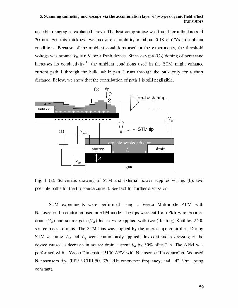
5. Scanning tunneling microscopy via the accumulation layer of p-type organic field effect transistors
unstable imaging as explained above. The best compromise was found for a thickness of
20 nm. For this thickness we measure a mobility of about 0.18 cm2/Vs in ambient
conditions. Because of the ambient conditions used in the experiments, the threshold
voltage was around Vth � 6 V for a fresh device. Since oxygen (O2) doping of pentacene
increases its conductivity,11 the ambient conditions used in the STM might enhance
current path 1 through the bulk, while part 2 runs through the bulk only for a short
distance. Below, we show that the contribution of path 1 is still negligible.
organic semiconductor
gate
source drain
dielectric
L
dVsg
Vsd
Vbias
feedback amp.
STM tip
Fig. 1 (a): Schematic drawing of STM and external power supplies wiring. (b): two
possible paths for the tip-source current. See text for further discussion.
STM experiments were performed using a Veeco Multimode AFM with
Nanoscope IIIa controller used in STM mode. The tips were cut from Pt/Ir wire. Source-
drain (Vsd) and source-gate (Vsg) biases were applied with two (floating) Keithley 2400
source-measure units. The STM bias was applied by the microscope controller. During
STM scanning Vsd and Vsg were continuously applied; this continuous stressing of the
device caused a decrease in source-drain current Isd by 30% after 2 h. The AFM was
performed with a Veeco Dimension 3100 AFM with Nanoscope IIIa controller. We used
Nanosensors tips (PPP-NCHR-50, 330 kHz resonance frequency, and ~42 N/m spring
constant).
dielectric- - - - - - - - - - - - - - - - -
e2
source + + + + + + + + + + + + +
1
tip
(a)
(b)
59

5.3 Results and discussion
The STM images taken on a pentacene oFET in the accumulation regime (Vsg –Vth
= -12 V and Vsd = 0 V) are shown in Figs. 2 a) and b). The STM settings were Vbias = 200
mV and Itunnel = 1.2 pA. In Fig. 2a, the source and drain electrodes are indicated; their
nominal height of 30 nm is found back both in AFM and STM. In Fig. 2b, an STM image
is taken in the channel region, i.e. on SiO2. The observed pentacene grain sizes of around
200 nm are consistent with those observed by AFM in Fig. 2d.
1 µm
sour
ce
drain
50 nm
100 nm 100 nm Fig. 2: STM pictures at Vbias = 200 mV, Itunnel = 1.2 pA, Vsg – Vth = -12 V and Vsd = 0 V of
(a) a bottom contact pentacene field effect transistor and (b) a zoom in the channel
region. AFM pictures of (c) pentacene on Au and (d) pentacene on SiO2. In all images,
the pentacene layer is 20 nm thick. The vertical scales are (a) 50 nm and (b-d) 25 nm.
The same holds for the smaller pentacene grain sizes (� 40 - 200 nm) as observed
on the Au contacts in Fig. 2c. Finally, the measured terrace height in both AFM and STM
(a) (b)
(c) (d)
60
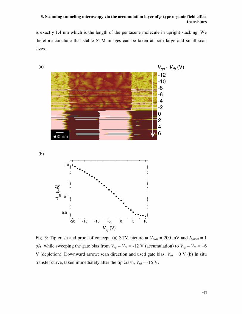
5. Scanning tunneling microscopy via the accumulation layer of p-type organic field effect transistors
is exactly 1.4 nm which is the length of the pentacene molecule in upright stacking. We
therefore conclude that stable STM images can be taken at both large and small scan
sizes.
Vsg - Vth (V)
500 nm
-12-10-8-6-4-20246
-20 -15 -10 -5 0 5 10
0.01
0.1
1
10
-I sd (µ
A)
Vsg
(V) Fig. 3: Tip crash and proof of concept. (a) STM picture at Vbias = 200 mV and Itunnel = 1
pA, while sweeping the gate bias from Vsg – Vth = -12 V (accumulation) to Vsg – Vth = +6
V (depletion). Downward arrow: scan direction and used gate bias. Vsd = 0 V (b) In situ
transfer curve, taken immediately after the tip crash, Vsd = -15 V.
(a)
(b)
61
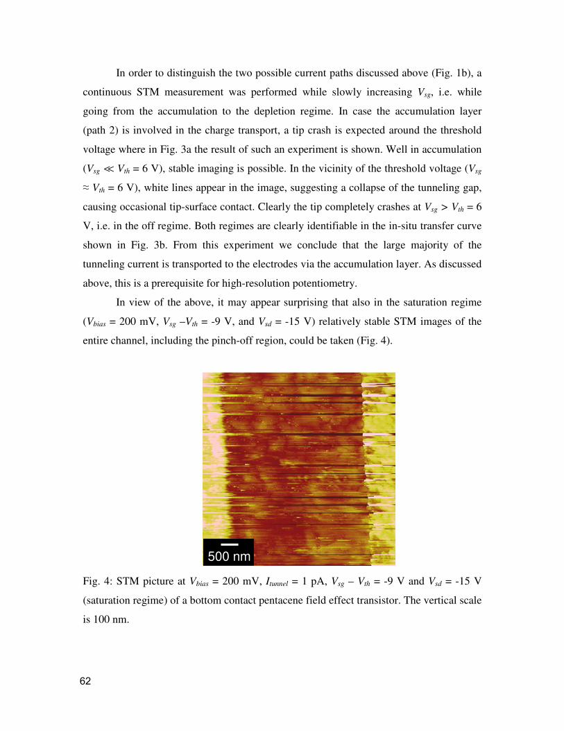
In order to distinguish the two possible current paths discussed above (Fig. 1b), a
continuous STM measurement was performed while slowly increasing Vsg, i.e. while
going from the accumulation to the depletion regime. In case the accumulation layer
(path 2) is involved in the charge transport, a tip crash is expected around the threshold
voltage where in Fig. 3a the result of such an experiment is shown. Well in accumulation
(Vsg � Vth = 6 V), stable imaging is possible. In the vicinity of the threshold voltage (Vsg
� Vth = 6 V), white lines appear in the image, suggesting a collapse of the tunneling gap,
causing occasional tip-surface contact. Clearly the tip completely crashes at Vsg > Vth = 6
V, i.e. in the off regime. Both regimes are clearly identifiable in the in-situ transfer curve
shown in Fig. 3b. From this experiment we conclude that the large majority of the
tunneling current is transported to the electrodes via the accumulation layer. As discussed
above, this is a prerequisite for high-resolution potentiometry.
In view of the above, it may appear surprising that also in the saturation regime
(Vbias = 200 mV, Vsg –Vth = -9 V, and Vsd = -15 V) relatively stable STM images of the
entire channel, including the pinch-off region, could be taken (Fig. 4).
500 nm
Fig. 4: STM picture at Vbias = 200 mV, Itunnel = 1 pA, Vsg – Vth = -9 V and Vsd = -15 V
(saturation regime) of a bottom contact pentacene field effect transistor. The vertical scale
is 100 nm.
62

5. Scanning tunneling microscopy via the accumulation layer of p-type organic field effect transistors
However, an occasional tip-surface contact seemed to occur. This can
qualitatively be understood from the fact that stable imaging in the saturation regime
should be possible when the current density injected from the tip is small as compared to
that in the channel. Under the conditions used, i.e. a 0.2 µA current and a 7 mm wide
channel, the surface current density in the channel is around 3×10⁻⁵ A/m, so the above
criterion translates into a minimal width of the Itunnel = 1 pA tip current at the
accumulation layer of about 35 nm. For an average layer thickness of 20 nm, a spread of
a few tens of nm seems to be at the edge of what can considered to be realistic. Hence, an
occasional tip-surface contact is to be expected, in line with experimental observations.
This spreading width is also the maximum attainable spatial resolution in STP. A value of
35 nm is about a factor three better than what can be reached with SKPM. Hence, for
optimal resolution current spreading should be suppressed and the organic layer thickness
should be as thin as possible. Although the latter also holds for SKPM, there is an
important difference between SKPM and STM. In the former technique, resolution is
limited by long range electrostatic interactions, which hardly change for very thin films,
see Chapter 4. Hence, reducing the film thickness to the nm level is expected to have a
much bigger effect on the STP resolution than on the SKPM resolution.
50 nm
Fig. 5: STM picture at Vbias = -200 mV, Itunnel = 1 pA, Vsg – Vth = -12 V and Vsd = 0 V in
the channel region. The vertical scale is 30 nm.
63
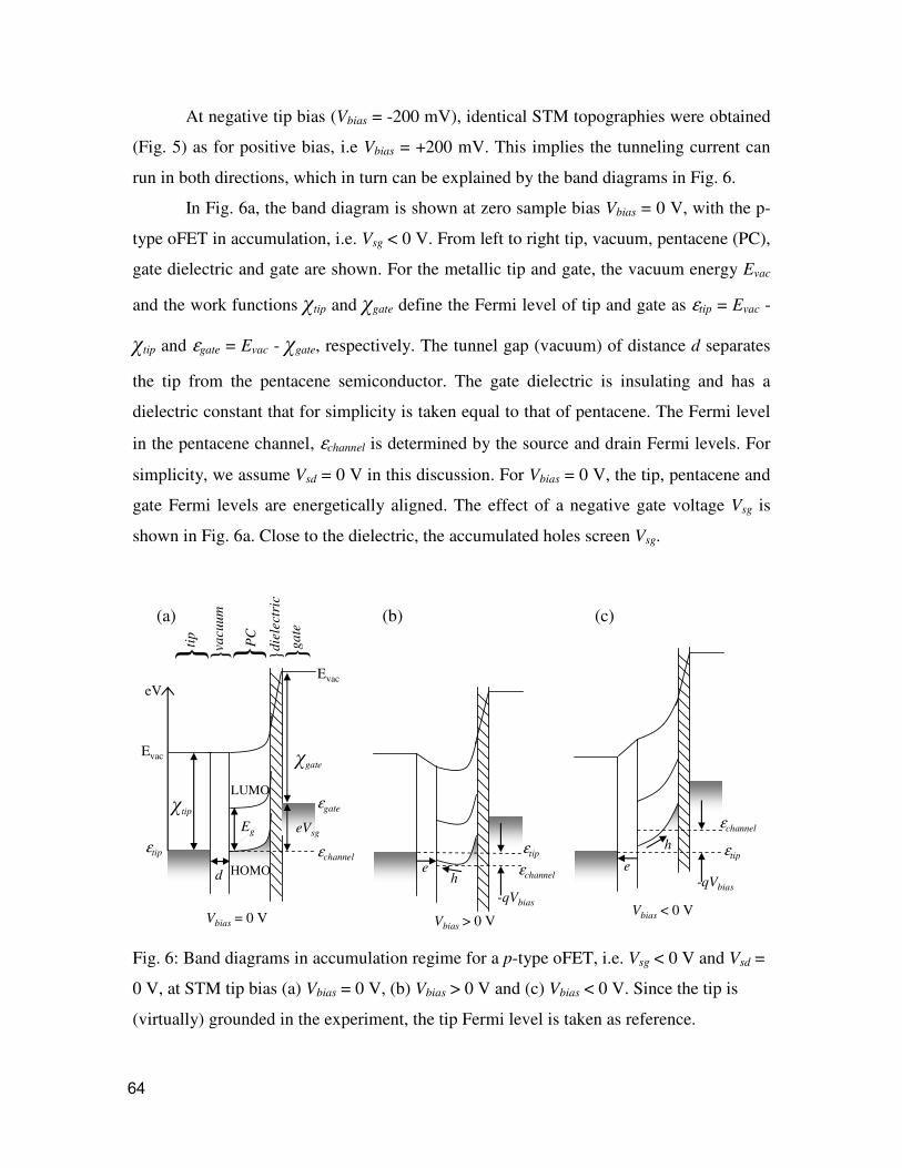
At negative tip bias (Vbias = -200 mV), identical STM topographies were obtained
(Fig. 5) as for positive bias, i.e Vbias = +200 mV. This implies the tunneling current can
run in both directions, which in turn can be explained by the band diagrams in Fig. 6.
In Fig. 6a, the band diagram is shown at zero sample bias Vbias = 0 V, with the p-
type oFET in accumulation, i.e. Vsg < 0 V. From left to right tip, vacuum, pentacene (PC),
gate dielectric and gate are shown. For the metallic tip and gate, the vacuum energy Evac
and the work functions �tip and �gate define the Fermi level of tip and gate as εtip = Evac -
�tip and εgate = Evac - �gate, respectively. The tunnel gap (vacuum) of distance d separates
the tip from the pentacene semiconductor. The gate dielectric is insulating and has a
dielectric constant that for simplicity is taken equal to that of pentacene. The Fermi level
in the pentacene channel, εchannel is determined by the source and drain Fermi levels. For
simplicity, we assume Vsd = 0 V in this discussion. For Vbias = 0 V, the tip, pentacene and
gate Fermi levels are energetically aligned. The effect of a negative gate voltage Vsg is
shown in Fig. 6a. Close to the dielectric, the accumulated holes screen Vsg.
�tip
Evac
εtip
Vbias = 0 V
d
LUMO
HOMO
tip } PC
}vacu
um} di
elec
tric
}
�gate
Evac
εgate
gate
}
Eg eVsg
εchannel
Vbias > 0 VVbias < 0 V
eeh
hεtip εtip
-qVbias
-qVbias
εchannel
εchannel
eV
Fig. 6: Band diagrams in accumulation regime for a p-type oFET, i.e. Vsg < 0 V and Vsd =
0 V, at STM tip bias (a) Vbias = 0 V, (b) Vbias > 0 V and (c) Vbias < 0 V. Since the tip is
(virtually) grounded in the experiment, the tip Fermi level is taken as reference.
(a) (b) (c)
64
5. Scanning tunneling microscopy via the accumulation layer of p-type organic field effect transistors
For positive sample bias Vbias > 0 V, the most probable current pathway is
illustrated in Fig. 6b. As shown, electrons tunnel from the tip to the HOMO of pentacene
where they recombine with holes coming from the accumulation layer. At negative
sample bias Vbias < 0 V, see Fig. 6c, electrons tunnel from the HOMO of pentacene to the
tip, creating vacant holes in pentacene, which are subsequently transported to the
accumulation layer.
To get an idea of the maximum current density that can be used in this type of
experiment, we followed the imaging stability versus tunnel current. By increasing the
STM current to Itunnel = 10 pA, the ‘topography’ started showing a flat surface, suggesting
that the STM tip penetrates the layer. At Itunnel = 20 pA the tip crashed on the SiO2
dielectric.
5.4 Conclusion
Summarizing, we demonstrate the possibility to do STM on operational oFETs in
both the linear and the saturation regime. The tunnel current is transported to the source
and drain contacts via the accumulation layer. With the condition of high signal-to-noise
ratio in the tunnel current, the demonstration of stable STM is an important step towards
high resolution scanning tunneling potentiometry.
5.5 References and notes
[1] P. Muralt, and D.W. Pohl, Appl. Phys. Lett. 48, 514 (1986).
[2] D.S.H. Charrier, T. de Vries, S.G.J. Mathijssen, E.-J. Geluk, E.C.P. Smits, M.
Kemerink, R.A.J. Janssen, Org. Electron. 10, 994 (2009).
[3] L. Bürgi, H. Sirringhaus, and R.H. Friend, Appl. Phys. Lett. 80, 2913 (2002).
[4] E.C.P. Smits, S.G.J. Mathijssen, M. Cölle, A.J.G. Mank, P.A. Bobbert, P.W.M. Blom,
B. de Boer, and D.M. de Leeuw, Phys. Rev. B 76, 125202 (2007).
65
[5] E. Mena-Osteritz, A. Meyer, B.M.W. Langeveld-Voss, R.A.J. Janssen, E.W. Meijer,
and P. Bäuerle, Angew. Chem. Int. Ed. 39, 2680 (2000).
[6] B. Grévin, P. Rannou, R. Payerne, A. Pron, and J.-P. Travers, Adv. Mater. 15, 881
(2003).
[7] G.R. Dholakia, M. Meyyappan, A. Facchetti, and T.J. Marks, Nano Lett. 6, 2447
(2006).
[8] A.I. Onipko, K.-F. Berggren, Yu.O. Klymenko, L.I. Malysheva, J.J.W. M. Rosink,
L.J. Geerligs, E. van der Drift, and S. Radelaar, Phys. Rev. B 61, 11118 (2000).
[9] L. Ruppel, A. Birkner, G. Witte, C. Busse, T. Lindner, G. Paasch, and C. Wöll, J.
Appl. Phys. 102, 033708 (2007).
[10] M. Kemerink, S.F. Alvarado, P. Muller, P.M. Koenraad, H.W.M. Salemink, J.H.
Wolter, and R.A.J. Janssen, Phys. Rev. B 70, 045202 (2004).
[11] O.D. Jurchescu, J. Baas, and T.T.M. Palstra, Appl. Phys. Lett. 87, 052102 (2005).
66
Chapter 6
Giant out-of-plane ambient actuation of poly(3,4-ethylenedioxythiophene) : poly(styrenesulfonate) thin films
6.1 Introduction
Conjugated polymers offer distinct and advantageous properties as compared to
inorganic materials in terms of plasticity, biocompatibility, and low processing cost.
Hence, their use in electroactive actuators attracts considerable interest,1-6 and finds
application in artificial muscles,7,8 microsystems,9 extendable textiles,10 and more recently
in lab-on-a-chip.11
Nowadays, the most widely used �-conjugated polymer in organic actuators is
polypyrrole (PPy), combined with dodecylbenzenesulfonate (DBS). This system
manifests an in-plane elongation that can be converted into a bending motion on micro or
millimetric scales with long lifetimes.12 The PPy:DBS system uses an additive electrolyte
as ionic reservoir, called ‘wet’ or ‘dry’ actuator if the reservoir is a liquid13 or a solid14
ion source. Under an externally applied voltage, the mobile anions or cations present in
the electrolyte can move and create a volume expansion (or contraction) in the polymer
by insertion (or de-insertion) of ions. Due to similarities, this expansion is also called
osmotic expansion.15 Additively, changes in bond lengths and conformation in the
polymer backbone may also contribute to expansion. In standard organic actuators, the
insertion and de-insertion of ions is achieved while maintaining global electroneutrality,
therefore the polymer is either oxidized or reduced. Although in-plane actuation is
67
commonly reported, remarkably few publications reported out-of-plane actuation. Smela
et al.16 measured a 1.5 µm thick film of PPy with atomic force microscopy (AFM),
showing an out-of-plane actuation of 125% at first cycle and 35% in normal cycle. The
experiment was done in a Na+DBS−-rich solution.
In the field of organic electronics, the oxidatively doped conjugated polycation
poly(3,4-ethylenedioxythiophene) blended with poly(styrenesulfonate) as polyanion
(PEDOT:PSS) is ubiquitous and a viable candidate for replacing metallic electrodes in
organic field effect transistors,17,18 organic solar cells,19 and organic light emitting
diodes.20 Recently, Kiefer et al.21 made a PEDOT bilayer in-plane actuator by
electrochemical synthesis and obtained good lifetime performances. They showed a high
deflection (1.5 mm) at a polymerization potential of 1.0 V and reasonable stability after
100 cycles. Out-of-plane actuation at ambient conditions of PEDOT:PSS thin films has
not been reported to our knowledge.
In this chapter, we present the surprising giant out-of-plane actuation (up to 950%
at first cycle and more than 100% for normal cycle) of PEDOT:PSS thin films in air,
without using additional ionic electrolytes. The PEDOT:PSS thin films deposited on
micropatterned electrodes actuate on the positive electrode upon application of a DC bias
with an onset bias around 4 V. Below we outline the experimental observations and a
possible mechanism for this remarkable actuation.
6.2 Results
6.2.1 Out-of-plane actuation at the anode
Thin (65 nm) PEDOT:PSS (1:6 weight ratio) films have been applied onto glass
substrates covered with interdigitating gold electrodes (30 nm high, 10 µm wide) at
variable spacing L (1, 4, 10, or 20 µm). Fig. 1a shows a typical example of the current
measured between anode and cathode (for L = 10 µm) while 4 V was applied. The current
decreases irregularly with time, suggesting that several processes are involved, to reach a
68
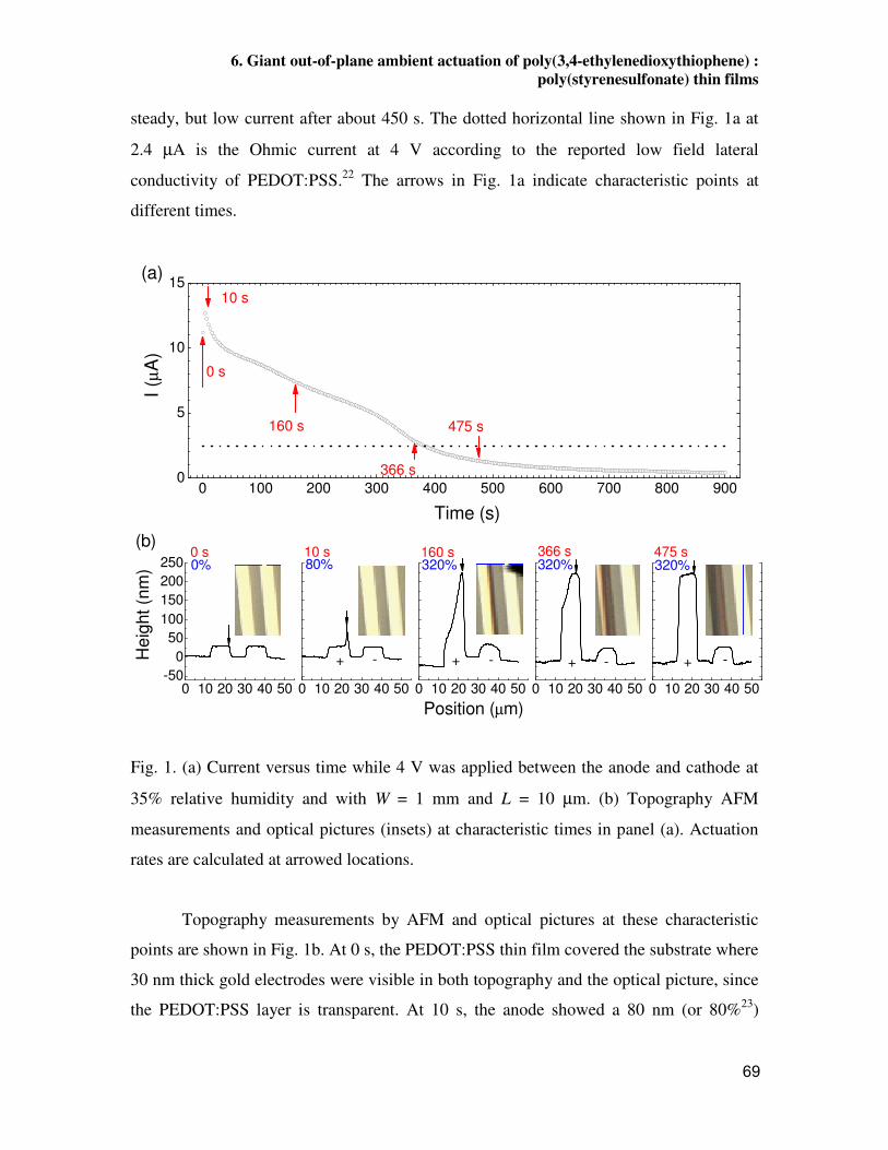
6. Giant out-of-plane ambient actuation of poly(3,4-ethylenedioxythiophene) : poly(styrenesulfonate) thin films
steady, but low current after about 450 s. The dotted horizontal line shown in Fig. 1a at
2.4 µA is the Ohmic current at 4 V according to the reported low field lateral
conductivity of PEDOT:PSS.22 The arrows in Fig. 1a indicate characteristic points at
different times.
0 100 200 300 400 500 600 700 800 9000
5
10
15
I (µA
)
Time (s)
0 s
160 s 475 s
366 s
10 s
(a)
0 10 20 30 40 50-50
050
100150200250
0 10 20 30 40 50 0 10 20 30 40 50 0 10 20 30 40 50 0 10 20 30 40 50
Hei
ght (
nm)
-
160 s
+ -+
320%366 s
Position (µm)
-+
320%475 s
320%80%0%10 s
0 s
-+
(b)
Fig. 1. (a) Current versus time while 4 V was applied between the anode and cathode at
35% relative humidity and with W = 1 mm and L = 10 µm. (b) Topography AFM
measurements and optical pictures (insets) at characteristic times in panel (a). Actuation
rates are calculated at arrowed locations.
Topography measurements by AFM and optical pictures at these characteristic
points are shown in Fig. 1b. At 0 s, the PEDOT:PSS thin film covered the substrate where
30 nm thick gold electrodes were visible in both topography and the optical picture, since
the PEDOT:PSS layer is transparent. At 10 s, the anode showed a 80 nm (or 80%23)
69
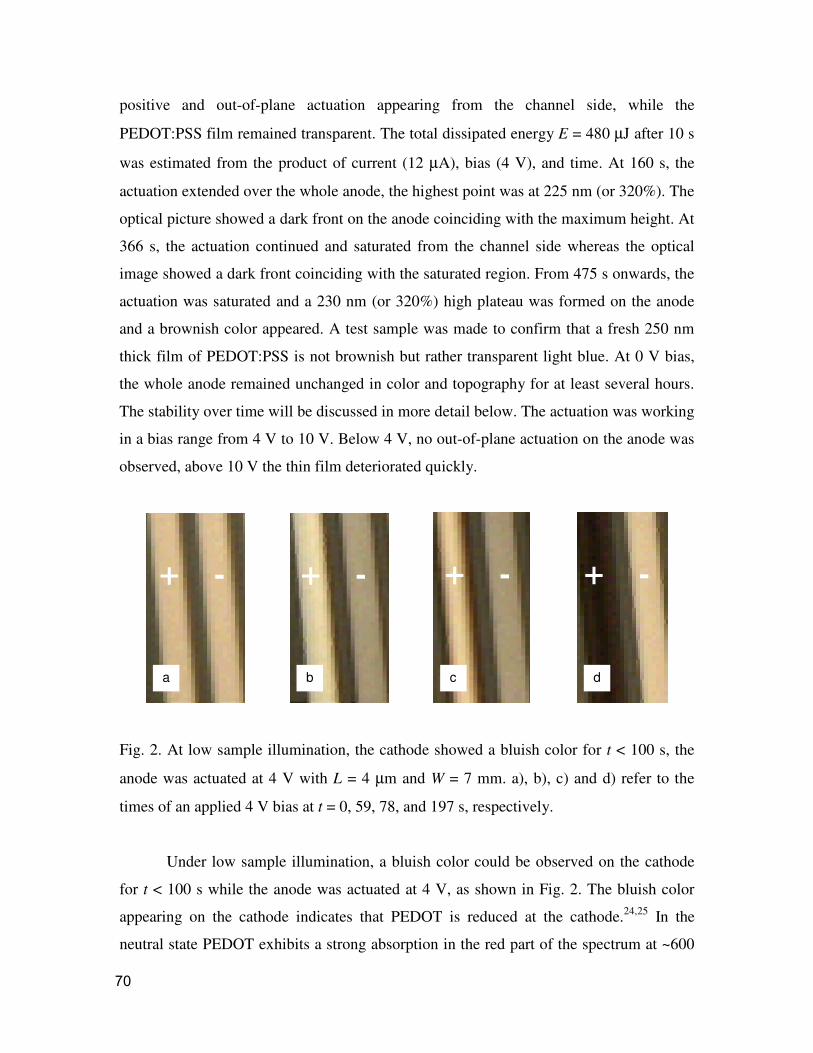
positive and out-of-plane actuation appearing from the channel side, while the
PEDOT:PSS film remained transparent. The total dissipated energy E = 480 µJ after 10 s
was estimated from the product of current (12 µA), bias (4 V), and time. At 160 s, the
actuation extended over the whole anode, the highest point was at 225 nm (or 320%). The
optical picture showed a dark front on the anode coinciding with the maximum height. At
366 s, the actuation continued and saturated from the channel side whereas the optical
image showed a dark front coinciding with the saturated region. From 475 s onwards, the
actuation was saturated and a 230 nm (or 320%) high plateau was formed on the anode
and a brownish color appeared. A test sample was made to confirm that a fresh 250 nm
thick film of PEDOT:PSS is not brownish but rather transparent light blue. At 0 V bias,
the whole anode remained unchanged in color and topography for at least several hours.
The stability over time will be discussed in more detail below. The actuation was working
in a bias range from 4 V to 10 V. Below 4 V, no out-of-plane actuation on the anode was
observed, above 10 V the thin film deteriorated quickly.
Fig. 2. At low sample illumination, the cathode showed a bluish color for t < 100 s, the
anode was actuated at 4 V with L = 4 µm and W = 7 mm. a), b), c) and d) refer to the
times of an applied 4 V bias at t = 0, 59, 78, and 197 s, respectively.
Under low sample illumination, a bluish color could be observed on the cathode
for t < 100 s while the anode was actuated at 4 V, as shown in Fig. 2. The bluish color
appearing on the cathode indicates that PEDOT is reduced at the cathode.24,25 In the
neutral state PEDOT exhibits a strong absorption in the red part of the spectrum at ~600
a b c d
+ - + - + - + -
70
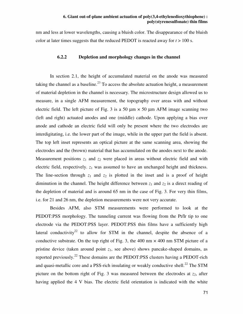
6. Giant out-of-plane ambient actuation of poly(3,4-ethylenedioxythiophene) : poly(styrenesulfonate) thin films
nm and less at lower wavelengths, causing a bluish color. The disappearance of the bluish
color at later times suggests that the reduced PEDOT is reacted away for t > 100 s.
6.2.2 Depletion and morphology changes in the channel
In section 2.1, the height of accumulated material on the anode was measured
taking the channel as a baseline.23 To access the absolute actuation height, a measurement
of material depletion in the channel is necessary. The microstructure design allowed us to
measure, in a single AFM measurement, the topography over areas with and without
electric field. The left picture of Fig. 3 is a 50 µm × 50 µm AFM image scanning two
(left and right) actuated anodes and one (middle) cathode. Upon applying a bias over
anode and cathode an electric field will only be present where the two electrodes are
interdigitating, i.e. the lower part of the image, while in the upper part the field is absent.
The top left inset represents an optical picture at the same scanning area, showing the
electrodes and the (brown) material that has accumulated on the anodes next to the anode.
Measurement positions z1 and z2 were placed in areas without electric field and with
electric field, respectively. z1 was assumed to have an unchanged height and thickness.
The line-section through z1 and z2 is plotted in the inset and is a proof of height
diminution in the channel. The height difference between z1 and z2 is a direct reading of
the depletion of material and is around 65 nm in the case of Fig. 3. For very thin films,
i.e. for 21 and 26 nm, the depletion measurements were not very accurate.
Besides AFM, also STM measurements were performed to look at the
PEDOT:PSS morphology. The tunneling current was flowing from the Pt/Ir tip to one
electrode via the PEDOT:PSS layer. PEDOT:PSS thin films have a sufficiently high
lateral conductivity22 to allow for STM in the channel, despite the absence of a
conductive substrate. On the top right of Fig. 3, the 400 nm × 400 nm STM picture of a
pristine device (taken around point z1, see above) shows pancake-shaped domains, as
reported previously.22 These domains are the PEDOT:PSS clusters having a PEDOT-rich
and quasi-metallic core and a PSS-rich insulating or weakly conductive shell.22 The STM
picture on the bottom right of Fig. 3 was measured between the electrodes at z2, after
having applied the 4 V bias. The electric field orientation is indicated with the white
71

arrow. The STM pictures show that the surface morphology in the channel changed from
pancake shaped clusters to fibrous shapes in going from a pristine to a fully actuated
device. The fibrous orientation coincides with the electric field direction. Moreover, the
STM pictures show a major field induced surface change, indicating mass transport
supported by the height reduction seen by AFM. Moreover, the bias needed for STM
measurements on actuated material was 3 times higher than for pristine material. By
measuring the I-V curves before and after actuation, we observed a decrease in film
conductance by one order of magnitude. This observation is consistent with the depletion
measurements, i.e. less material present in the channel will lead to a layer with a lower
conductance. The conductivity of the remaining material could not be accurately
determined because of a large (relative) uncertainty in the final layer thickness.
Fig. 3: Left picture: 50 µm × 50 µm AFM picture (zscale = 150 nm) scanning two (left and
right) actuated anodes and one (middle) cathode. A 4 V bias was applied during 30 min.
Top left inset: optical picture of the same area. z1 and z2 are placed in areas without and
with electric field, respectively. A cross-section on the line through z1 and z2 is plotted in
the inset with vertical axis in nm and horizontal axis in µm. On the right: 400 nm × 400
nm STM pictures (zscale = 30 nm) were measured at z1 and z2. z1 (z2) was taken with the
following parameters: sample bias 0.5 V (1.5 V), setpoint current 500 fA (100 fA).
72

6. Giant out-of-plane ambient actuation of poly(3,4-ethylenedioxythiophene) : poly(styrenesulfonate) thin films
6.2.3 Lack of volume conservation
The AFM measurements in Fig. 1b show that the final height of the anode after
actuation equals 230 nm. On first sight, this might be a summation of depleted material
from channel (65 nm) and cathode (65 nm) plus material already present on the anode (65
nm) plus the electrode thickness (30 nm), i.e. 230 � 225 = 65 + 65 + 65 + 30. Recall that
height is measured with respect to the surrounding channel, so the calculated 225 nm is
an upper limit under the assumption that both channel and cathode are fully depleted. For
L = 10 µm no further geometrical corrections are needed since channel and electrode
have the same width. The difference 230 − 225 = 5 nm is small in this case.
Surprisingly, however, the maximum attainable height on the anode proved to be
virtually independent of both channel length L and initial film thickness d, as shown in
Fig. 4. We attribute the non-systematic, minor variation between layers of different
thickness to differences in ambient humidity while measuring different samples. On a
very wide anode (not shown) the actuation stopped after certain length because the
channel was depleted and the reaction that started at the anode edge stopped. A very wide
cathode (not shown) did not change the maximum actuation height on the anode,
suggesting that the amount of material per unit length determines the final height.
This independence of d translates into giant actuation rates for very thin films, e.g.
950% for a 21 nm film. For these thinner films, the difference between anodic height
increase and available material (in channel and cathode regions) can be as high as 150
nm. From this result we conclude that a significant part of the height increase on the
anode is not due to a rearrangement of material but due to a volume increase of the
available material.
PEDOT:PSS films with a weight ratio 1:20 (instead of the 1:6 used above) and
with thicknesses of 42, 94, and 160 nm, respectively gave maximum actuation heights at
245 nm, 238 nm and 220 nm. Error bars were 5 nm for each value. Like for the 1:6
PEDOT:PSS, the maximally attainable actuation height seems mostly independent of film
73
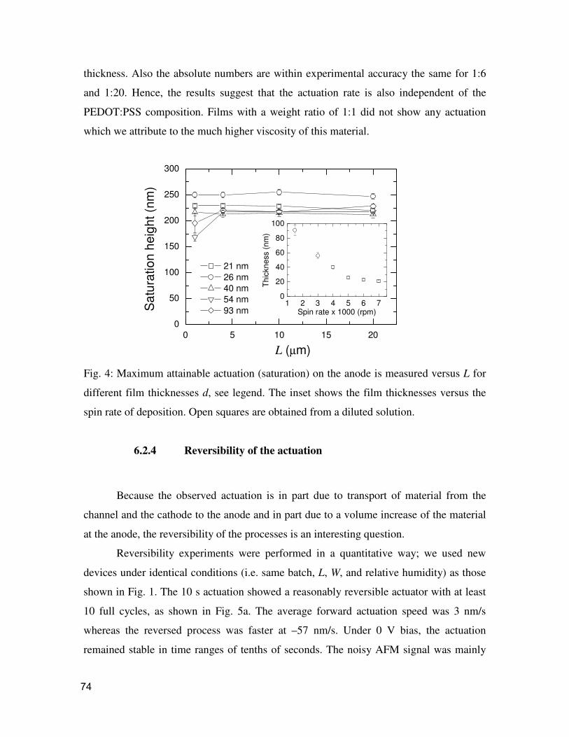
thickness. Also the absolute numbers are within experimental accuracy the same for 1:6
and 1:20. Hence, the results suggest that the actuation rate is also independent of the
PEDOT:PSS composition. Films with a weight ratio of 1:1 did not show any actuation
which we attribute to the much higher viscosity of this material.
0 5 10 15 200
50
100
150
200
250
300
1 2 3 4 5 6 70
20
40
60
80
100
Thi
ckne
ss (n
m)
Spin rate x 1000 (rpm)
Sat
urat
ion
heig
ht (n
m)
L (µm)
21 nm 26 nm 40 nm 54 nm 93 nm
Fig. 4: Maximum attainable actuation (saturation) on the anode is measured versus L for
different film thicknesses d, see legend. The inset shows the film thicknesses versus the
spin rate of deposition. Open squares are obtained from a diluted solution.
6.2.4 Reversibility of the actuation
Because the observed actuation is in part due to transport of material from the
channel and the cathode to the anode and in part due to a volume increase of the material
at the anode, the reversibility of the processes is an interesting question.
Reversibility experiments were performed in a quantitative way; we used new
devices under identical conditions (i.e. same batch, L, W, and relative humidity) as those
shown in Fig. 1. The 10 s actuation showed a reasonably reversible actuator with at least
10 full cycles, as shown in Fig. 5a. The average forward actuation speed was 3 nm/s
whereas the reversed process was faster at –57 nm/s. Under 0 V bias, the actuation
remained stable in time ranges of tenths of seconds. The noisy AFM signal was mainly
74
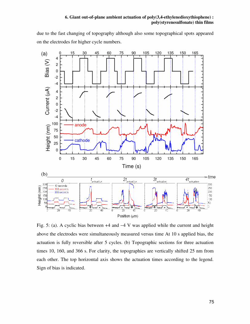
6. Giant out-of-plane ambient actuation of poly(3,4-ethylenedioxythiophene) : poly(styrenesulfonate) thin films
due to the fast changing of topography although also some topographical spots appeared
on the electrodes for higher cycle numbers.
0 15 30 45 60 75 90 105 120 135 150 165
0
25
50
75
100
-4
-2
0
2
4
-4
-2
0
2
40 15 30 45 60 75 90 105 120 135 150 165
anode
cathode
Hei
ght (
nm)
Time (s)
Cur
rent
(µA
)
Bia
s (V
)(a)
Fig. 5: (a). A cyclic bias between +4 and −4 V was applied while the current and height
above the electrodes were simultaneously measured versus time At 10 s applied bias, the
actuation is fully reversible after 5 cycles. (b) Topographic sections for three actuation
times 10, 160, and 366 s. For clarity, the topographies are vertically shifted 25 nm from
each other. The top horizontal axis shows the actuation times according to the legend.
Sign of bias is indicated.
(b)
75
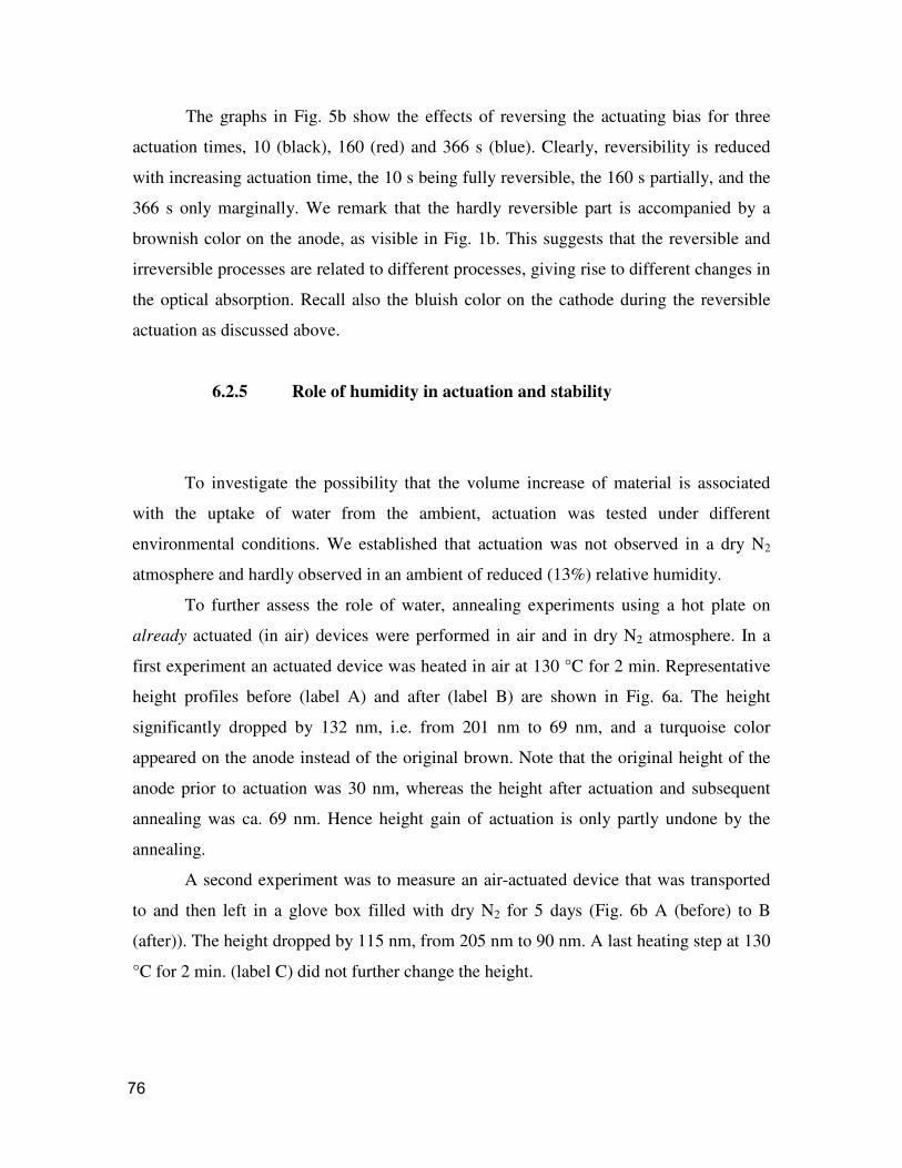
The graphs in Fig. 5b show the effects of reversing the actuating bias for three
actuation times, 10 (black), 160 (red) and 366 s (blue). Clearly, reversibility is reduced
with increasing actuation time, the 10 s being fully reversible, the 160 s partially, and the
366 s only marginally. We remark that the hardly reversible part is accompanied by a
brownish color on the anode, as visible in Fig. 1b. This suggests that the reversible and
irreversible processes are related to different processes, giving rise to different changes in
the optical absorption. Recall also the bluish color on the cathode during the reversible
actuation as discussed above.
6.2.5 Role of humidity in actuation and stability
To investigate the possibility that the volume increase of material is associated
with the uptake of water from the ambient, actuation was tested under different
environmental conditions. We established that actuation was not observed in a dry N2
atmosphere and hardly observed in an ambient of reduced (13%) relative humidity.
To further assess the role of water, annealing experiments using a hot plate on
already actuated (in air) devices were performed in air and in dry N2 atmosphere. In a
first experiment an actuated device was heated in air at 130 °C for 2 min. Representative
height profiles before (label A) and after (label B) are shown in Fig. 6a. The height
significantly dropped by 132 nm, i.e. from 201 nm to 69 nm, and a turquoise color
appeared on the anode instead of the original brown. Note that the original height of the
anode prior to actuation was 30 nm, whereas the height after actuation and subsequent
annealing was ca. 69 nm. Hence height gain of actuation is only partly undone by the
annealing.
A second experiment was to measure an air-actuated device that was transported
to and then left in a glove box filled with dry N2 for 5 days (Fig. 6b A (before) to B
(after)). The height dropped by 115 nm, from 205 nm to 90 nm. A last heating step at 130
°C for 2 min. (label C) did not further change the height.
76
6. Giant out-of-plane ambient actuation of poly(3,4-ethylenedioxythiophene) : poly(styrenesulfonate) thin films
0 10 20 30 40
0
50
100
150
200
250
300
BHei
ght (
nm)
Position (µm)
A
in air 201 nm
130 ºC for 2 min
(a)
69 nm
0 10 20 30 40
0
50
100
150
200
250
B
C
Hei
ght (
nm)
Position (µm)
206 nm
A
in N2130 °C (2 min)
90 nm
89 nm
5 days
(b)
0 5 10 15 20
0
50
100
150
200
250
0 300 600 900100
150
200
250
020406080100
nm
min
%H
eigh
t (nm
)
Position(µm)
Time
(c)
Fig. 6: Annealing experiments in air (a) and in N2 (b) of devices previously actuated in
air. The relaxation of the actuation or is shown in panel (c). Curves were recorded every
60 min during 4 days. The inset shows the height in nm (continuous curve) in the middle
of the anode and the relative humidity in % (open squares) versus time.
77
The absence of actuation in dry environments already indicates that ambient water
is involved in the actuation, either directly by enabling electrochemical reactions, or
indirectly by acting as a plasticizer for PEDOT:PSS. The very similar effects of slow and
forced drying, i.e. a height reduction on the actuated anode while the cathode remains
unchanged, suggest that a significant fraction (~60%) of the gained height is due to
hygroscopic effects, i.e. absorbed water. The material remaining on the anode after
evaporation of excess water has likely been transported from the channel and cathode, as
discussed under in section 2.2 above.
Another experiment was the continuous height measurement under ambient
conditions during 4 days (Fig. 6c). The inset shows the height (continuous curve) in the
middle of the anode versus time, empty squares are the ambient relative humidity
recorded simultaneously. In addition to a drop by 100 nm of the actuated height over 4
days, a color change from brownish to turquoise was observed.
6.2.6 Surface potential measurements
Scanning Kelvin probe microscopy measurements (SKPM) were performed on
different samples. Typical results for a device with film thickness of 21 nm are shown in
Fig. 7 (black). Fig. 7a shows the simultaneously measured topography and surface
potential averaged over the anode (continuous line) and cathode (dotted line) versus time.
In regions 1 and 2, a 4 V bias is applied, while in regions 0 and 3 both electrodes
are grounded. Surprisingly, the surface potential of both electrodes is roughly equal
(Vanode − Vcathode � 0.4 V) despite a bias voltage of 4 V between them (region 1 in Fig. 7a).
Once saturation is reached (at t = 413 s, region 2) a relatively sudden drop of both surface
potentials is observed. 65 nm and 91 nm (red) thick films exhibited similar surface
potential behavior, though with a significantly smaller difference of surface potentials
between the electrodes (Vanode − Vcathode � 0.2 V) in region 1, i.e. during actuation.
78
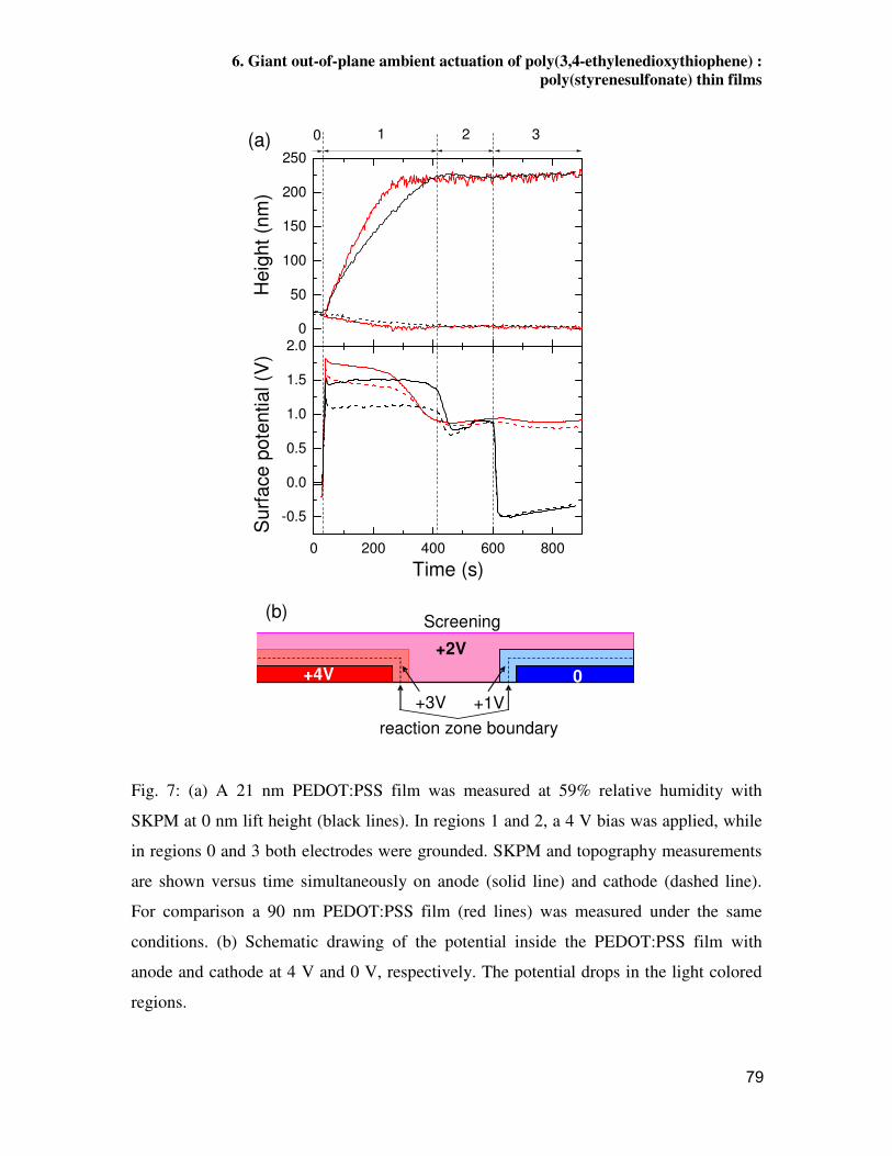
6. Giant out-of-plane ambient actuation of poly(3,4-ethylenedioxythiophene) : poly(styrenesulfonate) thin films
0 200 400 600 800
-0.5
0.0
0.5
1.0
1.5
2.00
50
100
150
200
250
Sur
face
pot
entia
l (V
)
Time (s)
0 1 2 3
Hei
ght (
nm)
(a)
+3V +1Vreaction zone boundary
Screening
+4V 0
+2V
(b)
Fig. 7: (a) A 21 nm PEDOT:PSS film was measured at 59% relative humidity with
SKPM at 0 nm lift height (black lines). In regions 1 and 2, a 4 V bias was applied, while
in regions 0 and 3 both electrodes were grounded. SKPM and topography measurements
are shown versus time simultaneously on anode (solid line) and cathode (dashed line).
For comparison a 90 nm PEDOT:PSS film (red lines) was measured under the same
conditions. (b) Schematic drawing of the potential inside the PEDOT:PSS film with
anode and cathode at 4 V and 0 V, respectively. The potential drops in the light colored
regions.
79
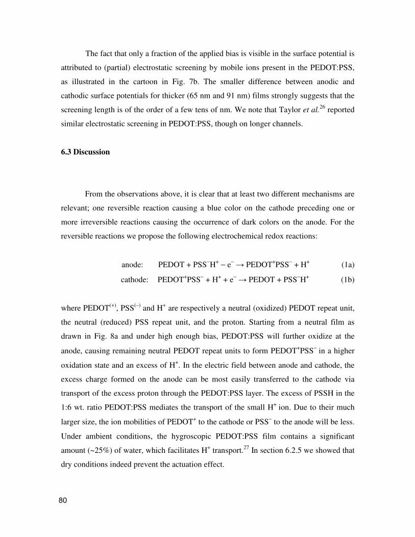
The fact that only a fraction of the applied bias is visible in the surface potential is
attributed to (partial) electrostatic screening by mobile ions present in the PEDOT:PSS,
as illustrated in the cartoon in Fig. 7b. The smaller difference between anodic and
cathodic surface potentials for thicker (65 nm and 91 nm) films strongly suggests that the
screening length is of the order of a few tens of nm. We note that Taylor et al.26 reported
similar electrostatic screening in PEDOT:PSS, though on longer channels.
6.3 Discussion
From the observations above, it is clear that at least two different mechanisms are
relevant; one reversible reaction causing a blue color on the cathode preceding one or
more irreversible reactions causing the occurrence of dark colors on the anode. For the
reversible reactions we propose the following electrochemical redox reactions:
anode: PEDOT + PSS−H+ − e− � PEDOT+PSS− + H+ (1a)
cathode: PEDOT+PSS− + H+ + e− � PEDOT + PSS−H+ (1b)
where PEDOT(+), PSS(–) and H+ are respectively a neutral (oxidized) PEDOT repeat unit,
the neutral (reduced) PSS repeat unit, and the proton. Starting from a neutral film as
drawn in Fig. 8a and under high enough bias, PEDOT:PSS will further oxidize at the
anode, causing remaining neutral PEDOT repeat units to form PEDOT+PSS− in a higher
oxidation state and an excess of H+. In the electric field between anode and cathode, the
excess charge formed on the anode can be most easily transferred to the cathode via
transport of the excess proton through the PEDOT:PSS layer. The excess of PSSH in the
1:6 wt. ratio PEDOT:PSS mediates the transport of the small H+ ion. Due to their much
larger size, the ion mobilities of PEDOT+ to the cathode or PSS− to the anode will be less.
Under ambient conditions, the hygroscopic PEDOT:PSS film contains a significant
amount (~25%) of water, which facilitates H+ transport.27 In section 6.2.5 we showed that
dry conditions indeed prevent the actuation effect.
80
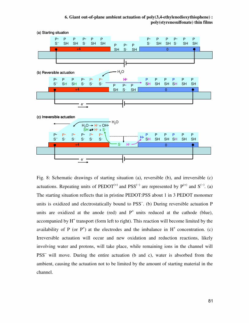
6. Giant out-of-plane ambient actuation of poly(3,4-ethylenedioxythiophene) : poly(styrenesulfonate) thin films
(a) Starting situation
(b) Reversible actuation
PSH
P+
S−PSH
PSH
PSH
P+
S−PSH
PSH
PSH
P+
S−PSH
P+
S−P+
S−PSH
PSH+4 0
P+
S−P+
S−P+
S−PSH
PSH
P+
S−PSH
PSH
PSH
PSH
PSH
PSHP+
S−PSH
PSH+4 0
e−
H+
H2O
(c) Irreversible actuation
P+
S−P+
S−P+
S−P+
S−P+
S−P+
S−PSH
PSH
PSH
PSH
PSH
PSH
S−+4 0
e−
H2O
H+
H•
SH H+ + S−H2O H+ + OH•
(a) Starting situation
(b) Reversible actuation
PSH
P+
S−PSH
PSH
PSH
P+
S−PSH
PSH
PSH
P+
S−PSH
P+
S−P+
S−PSH
PSH+4 0
PSH
P+
S−PSH
PSH
PSH
P+
S−PSH
PSH
PSH
P+
S−PSH
P+
S−P+
S−PSH
PSH+4 0
P+
S−P+
S−P+
S−PSH
PSH
P+
S−PSH
PSH
PSH
PSH
PSH
PSHP+
S−PSH
PSH+4 0
e−
H+
H2O
P+
S−P+
S−P+
S−PSH
PSH
P+
S−PSH
PSH
PSH
PSH
PSH
PSHP+
S−PSH
PSH+4 0
e−
H+
H2O
(c) Irreversible actuation
P+
S−P+
S−P+
S−P+
S−P+
S−P+
S−PSH
PSH
PSH
PSH
PSH
PSH
S−+4 0
e−
H2O
H+
H•
SH H+ + S−H2O H+ + OH•
(c) Irreversible actuation
P+
S−P+
S−P+
S−P+
S−P+
S−P+
S−PSH
PSH
PSH
PSH
PSH
PSH
S−+4 0
e−
H2O
H+
H•
SH H+ + S−H2O H+ + OH•
Fig. 8: Schematic drawings of starting situation (a), reversible (b), and irreversible (c)
actuations. Repeating units of PEDOT(+) and PSS(−) are represented by P(+) and S(−). (a)
The starting situation reflects that in pristine PEDOT:PSS about 1 in 3 PEDOT monomer
units is oxidized and electrostatically bound to PSS−. (b) During reversible actuation P
units are oxidized at the anode (red) and P+ units reduced at the cathode (blue),
accompanied by H+ transport (form left to right). This reaction will become limited by the
availability of P (or P+) at the electrodes and the imbalance in H+ concentration. (c)
Irreversible actuation will occur and new oxidation and reduction reactions, likely
involving water and protons, will take place, while remaining ions in the channel will
PSS− will move. During the entire actuation (b and c), water is absorbed from the
ambient, causing the actuation not to be limited by the amount of starting material in the
channel.
81
Reaction (1b) is the electrochemical reduction of PEDOT+, the reverse of (1a),
and proposed to occur at the cathode. The proton is supplied by the anodic reaction and
forms PSSH with PSS−, while PEDOT+ is (partially) reduced to PEDOT. The observation
of a bluish color on the cathode confirms this reduction step for times t < 100 s. For
longer times, the working conditions enable the oxidation of PEDOT by oxygen from the
air:
O2 + 4 PEDOT + 4 PSS−H+ � 2 H2O + 4 PEDOT+PSS− (2)
which suppresses the bluish color on the cathode for times t > 100 s.
Having established possible redox reactions, we will now discuss the actuation
mechanism. The actuation on the anode may be caused by (a) a mass transport of anions
coming from the cathode, (b) conformational changes, or (c) osmosis, i.e. uptake of H2O
from ambient air or other parts of the film. An alternative to the three mentioned reasons
for explaining the apparent volume expansion is gas formation due to electrolysis of
water. As demonstrated by de Brito et al.28 a PEDOT:PSS layer sandwiched by crossed
Au electrodes can be used as (irreversible) fuse due to the trapping of gas between the
electrodes. However, in the present case, gas formation is not consistent with the
observed reversibility of actuation, gas formation being irreversible.
The proposed redox reactions (1a) and (1b) do not involve anionic species to
transport from the cathode toward the anode. Apart from PEDOT+, PSS−, and H+, the
most abundant ionic species in PEDOT:PSS is Na+ (300 ppm). Lowering the Na+
concentration by a factor 10 to 30 ppm did not lead to appreciable changes in actuation.
Doping of polymer chains is known to induce conformational changes. X-ray
measurements on highly oriented polyacetylene showed a chain length elongation (or
contraction) upon Li+, K+ donor (or I− acceptor) doping.29 However, the reported effects
are typically small as compared to the height changes observed here. Hence, in our view
neither mass transport (small protons) nor conformational changes can explain the
actuation on the anode. Therefore, we suggest the osmotic mechanism to explain the
actuation and, simultaneously, the apparent lack of volume conservation. Reaction (1a)
leads to an increased positive doping of PEDOT+ chains at the anode, causing the further
82
6. Giant out-of-plane ambient actuation of poly(3,4-ethylenedioxythiophene) : poly(styrenesulfonate) thin films
uptake of ambient H2O. Alternatively, other parts of the thin film may act as source for
H2O. The assignment of H2O uptake on the anode as the main cause of volume increase is
in full agreement with the observations in described in section 6.2.5.
By changing the bias polarity, reactions (1) swap electrode, and the PEDOT+
concentration on the ‘new’ anode increases at the cost of the concentration on the ‘old’
anode. Hence, an osmotic driving force for H2O transport from the old to the new anode
develops, making the actuation reversible. A schematic drawing of the reversible process
is shown in Fig. 8b.
Several mechanisms can be proposed as for why reactions (1a) and (1b) stop and
irreversible reactions start. E.g. when all PEDOT becomes fully neutralized at the cathode
or fully oxidized at the anode, reactions (1b) and (1a) will terminate. The former option
seems less likely because air oxidation (2) enables a ‘recycling’ of neutralized PEDOT
under ambient conditions at the cathode. Both options, however, also seem unlikely
considering that the integrated current during the reversible regime is insufficient to
convert all available PEDOT on the anode or PEDOT+ on the cathode. More likely,
reactions (1a) and (1b) stop because of a pH imbalance developing between the two
electrodes. At that point other redox reactions can take over that can restore the pH
balance and are within the electrochemical window, e.g.
anode: H2O − e− � H+ + OH (3a)
2 H2O − 4 e− � 4 H+ + O2 (3b)
cathode: H+ + e− � H· (3c)
2 H+ + 2e− � H2 (3d)
where reactions (3a) and (3c) are equivalent to (3b) and (3d) but do not require the
overpotentials usually associated with the formation of gaseous oxygen or hydrogen. To
maintain charge neutrality above the electrodes, we propose the migration of PSS− to the
anode and migration of protons to the cathode. The observations described in section
6.2.2 are consistent with transport of PSS−. Once PSS− has left the cathode it leaves
behind a vacant H+, which will likely be reduced to form H· radicals that will react
further, making the process described by (3a) and (3c) irreversible. A schematic drawing
83

is shown in Fig. 8c. In this regime, the actuation is a combination of the reactions (1a)
and (3a) implying mass (PSS) transport and osmosis (uptake from water). The
observations in section 6.2.2 clearly showed a depleted channel after reaching the
maximum attainable actuation, showing that also the channel may act as PSS− source.
They also showed a morphology change in the channel attributed to transport of PSS to
the anode. The thermal and temporal experiments in section 6.2.5 showed a partial height
reduction reflecting the H2O component; the remaining material on the anode is therefore
attributed to PSS. The dark and turquoise colors are tentatively explained by the
irreversible chemical reactions of water or formed hydroxyl radicals at the anode to
highly oxidized PEDOT segments.
The picture sketched above rationalizes most observations. However, the
independence of the maximally attainable actuation height on channel width and film
thickness and on PEDOT:PSS ratio (section 6.2.3) remain to be explained. The answer to
these, at first sight surprising independencies comes from the SKPM experiments
discussed in section 6.2.6. From the thickness dependence of the potential screening we
concluded that the screening length is of the order of tens of nm. Consequently, only a
very thin (tens of nm) region is at sufficiently large voltage with respect to the rest of the
sample to enable electrochemical reactions, see Fig. 7b. Hence, only the reactive material
on the anode within the screening length can react. In other words, the screening length
rather than the film thickness determines the actuation height. A similar reasoning
explains the channel length independence: as long as the amount of material within the
screening length is the limiting factor, the final actuation height is independent of L. Only
for short channels the combined amount of material in the channel and on the cathode
may become limiting, as seems to happen in a few instances in Fig. 4. The PEDOT:PSS
ratio independence might be explained by a consideration about the most likely screening
species being protons. Since PSS is present in similar absolute concentrations in 1:20 and
1:6 PEDOT:PSS material, and is the main proton source, both compositions will have
similar screening lengths. Since the amount of PEDOT within the screening length is
lower for 1:20, one might expect less actuation for 1:20. However, other effects like
viscosity, as is the case for 1:1, will play a role as well.
84

6. Giant out-of-plane ambient actuation of poly(3,4-ethylenedioxythiophene) : poly(styrenesulfonate) thin films
6.4 Conclusion
In conclusion, we have found an unexpected out-of-plane actuation of
PEDOT:PSS thin films under ambient conditions. The maximum attainable actuation was
found to be independent of film thickness and composition and leads to a maximum
actuation at first cycle of 950% for a 21 nm thick film. On basis of a wide range of
experimental observations, we propose a qualitative electrochemical model. The latter
assumes a reversible regime in which proton transport is dominant, and an irreversible
regime in which PSS− transport dominates. In both regimes osmotic water adsorption is
responsible for a large fraction of the volume expansion.
6.5 Experimental
In total, 20 substrates, each containing 62 microstructured pairs of interdigitated
electrodes were made. Both anode (positive) and cathode (negative) were 10 µm wide,
the distance L separating the electrodes was 1, 4, 10 or 20 µm, whereas the channel width
W was 1, 7 or 19 mm. Glass substrates and Si/SiO2 wafers did not show different results.
The samples were manufactured using standard UV photolithography. Starting from
chemically cleaned substrates, 5 nm of Ti as adhesion layer and 25 nm of Au were
subsequently deposited on the developed photoresist by electron beam evaporation under
high vacuum conditions. A classical lift-off with acetone was done to remove the resist
and to reveal the microstructures.
In our experiments, PEDOT:PSS with a weight ratio 1:6 was purchased from H.
C. Starck (Baytron P VP Al 4083, recently renamed Clevios P Jet (OLED)). The Na+
concentration was 300 ppm. Alternatively, a 1:6 PEDOT:PSS suspension with a 30 ppm
Na+ concentration was tried and did not exhibit differences in terms of actuation
behavior. Prior to spin coating, 2 mL of PEDOT:PSS was taken in a syringe and filtered
through a 5 µm porous material (Schleicher & Schue, FP 30/5,0 CN-S). Film thickness
85
was varied by adjusting the spin rate and dilution as shown in the inset of Fig. 4. The
samples were annealed at 200 °C for 2 minutes in order to reduce water content and
create a compact layer. Film thicknesses were measured with a profilometer or an AFM.
The measured thicknesses varied 5 nm depending on the sample location. Other
PEDOT:PSS compositions 1:x were used with x = 1 and x = 20. The high viscosity of x =
1 did not allow filtering through porous material. For x = 1 no actuation was observed.
Between fabrication and measurement the samples were stored in a vacuum glass
container (10-2 mbar) or in a N2-filled glove box.
The AFM (and scanning Kelvin probe microscope - SKPM) was performed with a
Veeco Dimension 3100. Free software (Super Screen Recorder, version 2.0) was used to
capture optical images from the built-in camera as video file. We used Nanosensors tips
(PPP-NCHR-50, 330 kHz resonance frequency and ~42 N m−1 spring constant) for AFM
and Pt-coated Olympus tips (OMCL-AC240TM-B2, 70 kHz resonance frequency and ~2
N/m spring constant) for SKPM. The Scanning Tunneling Microscope (STM) was a
Veeco Multimode equipped with a low current pre-amp. The STM tips were cut from
Pt/Ir wire.
Current-voltage characteristics were measured using a Keithley 4200 parameter
analyzer, which was also used to provide biases and measure currents during scanning
probe experiments.
6.6 References and notes
[1] T. F. Otero, J. Mater. Chem. 19, 681 (2009).
[2] E. Smela, MRS Bulletin 33,197 (2008).
[3] G. M. Spinks, E. Smela, in Handbook of Conducting Polymers, 3rd Edition, Vol 2
(Eds: T.A. Skotheim, J.R. Reynolds), (CRC Press LLC, Boca Raton, Florida, 2007, Ch.
14).
[4] E. Smela, Adv. Mater. 15, 481 (2003).
86
6. Giant out-of-plane ambient actuation of poly(3,4-ethylenedioxythiophene) : poly(styrenesulfonate) thin films
[5] C. Immerstrand, K. Holmgren-Peterson, K.-E. Magnusson, E. Jager, M. Krogh, M.
Skoglund, A. Selbing, and O. Inganäs, MRS Bulletin 27, 461 (2002).
[6] R.H. Baughman, Synth. Met. 78, 339 (1996).
[7] T.F. Otero, and J.M. Sansiñena, Adv. Mater. 10, 491 (1998).
[8] L. Bay, K. West, P. Sommer-Larsen, S. Skaarup, and M. Benslimane, Adv. Mater. 15,
310 (2003).
[9] E.W.H. Jager, O. Inganäs, and I. Lundström, Science 288, 2335 (2000).
[10] F. Carpi, and D. De Rossi, IEEE Transactions on Information Technology in
Biomedicine 9, 295 (2005).
[11] S.B. Prakash, M. Urdaneta, M. Christophersen, E. Smela, and P. Abshire, Sens.
Actuators B Chem. 129, 699 (2008).
[12] J. Ding, D. Zhou, G. Spinks, G. Wallace, S. Forsyth, M. Forsyth, and D.
MacFarlane, Chem. Mater. 15, 2392 (2003).
[13] W. Lu, A.G. Fadeev, B.H. Qi, E. Smela, B.R. Mattes, J. Ding, G.M. Spinks, J.
Mazurkiewicz, D.Z. Zhou, G.G. Wallace, D.R. MacFarlane, S.A. Forsyth, and M.
Forsyth, Science 297, 983 (2002).
[14] K. Kaneto, M. Kaneko, Y. Min, and A.G. MacDiarmid, Synth. Met. 71, 2211 (1995).
[15] L. Bay, T. Jacobsen, S. Skaarup, and K. West, J. Phys. Chem. B 105, 8492 (2001).
[16] E. Smela, and N. Gadegaard, Adv. Mater. 11, 953 (1999).
[17] H. Rost, J. Ficker, J.S. Alonso, L. Leenders, and I. McCulloch, Synth. Met. 145, 83
(2004).
[18] H.J. Snaith, H. Kenrick, M. Chiesa, and R.H. Friend, Polymer 46, 2573 (2005).
[19] S.-I. Na, S.-S. Kim, J. Jo, and D.-Y. Kim, Adv. Mater. 20, 4061 (2008).
[20] P.A. Levermore, R. Jin, X. Wang, L. Chen, D.D.C. Bradley, and J.C. de Mello, J.
Mater. Chem. 18, 4414 (2008).
[21] R. Kiefer, D.G. Weis, J. Travas-Sejdic, G. Urban, and J. Heinze, Sens. Actuators B
Chem. 123, 379 (2007).
[22] A.M. Nardes, M. Kemerink, R.A.J. Janssen, J.A.M. Bastiaansen, N.M.M. Kiggen, B.
M.W. Langeveld, A.J.J.M. van Breemen, and M.M. de Kok, Adv. Mater. 19, 1196
(2007).
87
[23] Due to the absence of absolute baseline, the baseline was defined on the
PEDOT:PSS surface around the positive electrode where the material was assumed not to
completely deplete. This assumption enabled us to estimate the actuation rates RA (%).
They were calculated as RA=(A−T)/I where A is the apparent actuation height between the
highest point above the anode and the lowest point on substrate, T the electrode thickness,
and I the initial PEDOT:PSS film thickness.
[24] J.C. Gustafsson, B. Liedberg, and O. Inganäs, Solid State Ionics 69, 145 (1994).
[25] H.W. Heuer, R. Wehrmann, and S. Kirchmeyer, Adv. Funct. Mater. 12, 89 2002.
[26] D.M. Taylor, D. Morris, and J.A. Cambridge, Appl. Phys. Lett. 85, 5266 (2004).
[27] A.M. Nardes, M. Kemerink, M.M. de Kok, E. Vinken, K. Maturova, and R.A.J.
Janssen, Org. Electron. 9, 727 (2008).
[28] B.C. de Brito, E.C.P. Smits, P.A. van Hal, T.C.T. Geuns, B. de Boer, C.J.M.
Lasance, H.L. Gomes, and D.M. de Leeuw, Adv. Mater. 20, 3750 (2008).
[29] N.S. Murthy, L.W. Shacklette, and R.H. Baughman, J. Chem. Phys. 87, 2346 (1987).
88

Potentiometry on organic semiconductor devices
Summary
In this thesis, we are interested in the local electrical potential of operational
devices based on organic semiconductors. Potential profiles are measured using advanced
scanning probe techniques with the final aim to confront experimental data with charge
transport and device models. The motivation to do so is that spatially resolved potentials
give a true window on the actual internal operation of the device, rather than on its mere
external output.
In order to do so in a quantitative manner, the spatial resolution of the used
potential probe needs to be understood in detail. Ideally, one should not only be able to
predict the experimental response from a known theoretical prediction, but also to
recover the underlying ‘true’ potential profile from an experimental (broadened) profile.
The most commonly used probe in this respect is scanning Kelvin probe microscopy, or
SKPM, which combines the classical Kelvin probe with atomic force microscopy (AFM).
Hence, in the first part of this thesis, we have focused on this technique. In a later
chapter, the first steps towards an alternative, scanning tunneling microscope (STM)
based potential probing technique are set. The last chapter uses AFM, STM and SKPM to
investigate a surprising actuation effect of PEDOT:PSS thin films.
Non-contact potentiometry or scanning Kelvin probe microscopy is a widely used
technique to study charge injection and transport in (in)organic devices by measuring a
laterally resolved local potential. This technique suffers from the significant drawback
that experimentally obtained curves do generally not reflect the true potential profile in
the device due to non-local coupling between the probing tip and the device. In Chapter 2
we quantitatively explain the experimental SKPM response, and by doing so directly link
theoretical device models to real observables. In particular, the model quantitatively
explains the effects of the tip-sample distance and the dependence on the orientation of
89

the probing tip with respect to the device. This coarse approach requires a very long
calculation time.
The performance of organic light emitting field effect transistors (LEFET) is
strongly influenced by the width of the recombination zone. In Chapter 3, we present an
analytical model for the recombination profile. Assuming Langevin recombination, the
recombination zone width W is found to be given by 4.34W dδ= with d and δ the gate
dielectric and accumulation layer thicknesses respectively. The model compares
favorably to both numerical calculations and measured surface potential profiles of an
actual LEFET.
As explained in Chapter 3, in ambipolar organic field effect transistors (oFET) the
shape of the channel potential is intimately related to the recombination zone width W,
and hence to the electron-hole recombination strength. However, surface potentials as
measured by scanning Kelvin probe microscopy (SKPM) are distorted due to spurious
capacitive couplings. In Chapter 4, we develop a (de)convolution method with an
experimentally calibrated transfer function to reconstruct the actual surface potential from
a measured SKPM response and vice versa. This approach is much faster than the one
presented in Chapter 2. Using this scheme, we find W = 0.5 µm for a nickel dithiolene
oFET, which translates into a recombination rate that is two orders of magnitude below
the Langevin value.
In Chapter 5, we report a new method for investigating the local electrical
properties of organic field effect transistors with potentially unprecedented spatial
resolution. In particular, we show that it is possible to perform scanning tunneling
microscopy on the channel of an operational pentacene oFET, despite the absence of a
conducting substrate. Charge transport from the STM tip to the contacts occurs via a
three-step process of vacuum tunneling, followed by vertical transport to the
accumulation layer and lateral transport in the accumulation layer.
In Chapter 6, we demonstrate giant out-of-plane actuation of thin films of
poly(3,4-ethylenedioxythiophene):poly(styrenesulfonate) (PEDOT:PSS) under ambient
conditions. The actuation is driven by an electrical bias and resulting current between
interdigitated gold electrodes on glass which are placed below the PEDOT:PSS thin film.
We combine current measurements with optical, AFM, SKPM and STM measurements
90
on spin cast films. The actuation is found to be independent of film thickness and
composition and leads to a maximum actuation in the first cycle of 950% for a 21 nm
thick film in ambient. Two actuation regimes are identified. In the first regime, reversible
redox reactions occur and actuation is mainly due to osmotic effects brought about by an
increasing ion concentration on the anode. In the irreversible regime, secondary oxidation
reactions occur and mass transport to the anode becomes also important. The
independence of the maximally attainable actuation height on channel width and film
thickness and on PEDOT:PSS ratio is explained by screening inside the thin film. From
the thickness dependence of the potential screening we concluded that the screening
length is of the order of tens of nm. Hence, the screening length rather than the film
thickness determines the actuation height.
To summarize, we succeeded to resolve the resolution issues associated with
scanning Kelvin probe microscopy, thereby enabling a quantitative comparison of
measured and modeled surface potentials. The developed tools and insight is applied to
the potential in an ambipolar oFET where we used the experimental SKPM response to
investigate the recombination zone width W. As a next step, potentially unprecedented
spatial resolution on organic semiconductors might be achieved using scanning tunneling
potentiometry. The first step in this direction, stable STM operation on the channel of a
working oFET, has been established.
91

92
Potentiometrie op organische halfgeleider devices
Samenvatting
In dit proefschrift zijn we geïnteresseerd in de lokale elektrische potentiaal van
operationele devices op basis van organische halfgeleiders. Potentiaalprofielen zijn
gemeten met behulp van geavanceerde scanning probe technieken met het uiteindelijke
doel om de experimentele gegevens te vergelijken met ladingstransport- en
devicemodellen. De motivatie om dit te doen is dat ruimtelijk opgeloste potentialen een
kijk geven op de werkelijke interne werking van het device, en niet alleen op zijn externe
werking.
Om dit op een kwantitatieve wijze te doen moet de ruimtelijke resolutie van de
gebruikte potentiaalsensor in detail worden begrepen. Idealiter is men niet alleen in staat
om de experimentele respons op een bekende theoretische voorspelling te berekenen,
maar ook om het onderliggende 'echte' potentiaalprofiel te reconstrueren uit een
experimenteel (verbreed) profiel. De voor dit doel meest gebruikte sensor is scanning
Kelvin probe microscopie, of SKPM. Het combineert de klassieke Kelvin probe met
atomaire kracht microscopie (AFM). Vandaar dat we in het eerste deel van dit
proefschrift deze techniek bestuderen. In een later hoofdstuk worden de eerste stappen
gezet op weg naar een alternatieve techniek om potentialen te meten, gebaseerd op
scanning tunneling microscopie (STM). Het laatste hoofdstuk maakt gebruik van AFM,
STM en SKPM om een verrassend volumeveranderingseffect in dunne PEDOT:PSS
films te onderzoeken.
Contactloze potentiometrie of Kelvin scanning probe microscopie is een veel
gebruikte techniek om te ladingsinjectie en -transport in (in)organische devices te
bestuderen door het meten van lateraal opgeloste lokale potentialen. Deze techniek kampt
met het grote nadeel dat experimenteel verkregen curves meestal niet overeenkomen met
de echte potentiaalprofielen in het device. Dit is te wijten aan de niet-lokale
elektrostatische koppeling tussen de meetsonde en het device. In hoofdstuk 2 verklaren
we kwantitatief de experimentele SKPM respons, en leggen daarmee rechtstreeks
93
verband tussen theoretische devicemodellen en waarnemingen. In het bijzonder verklaart
het model kwantitatief de invloed van de tip-sample afstand en de afhankelijkheid van de
oriëntatie van de AFM tip ten opzichte van het device. Deze brute-kracht benadering
vereist zeer lange rekentijden.
Het gedrag van organische licht-emitterende veld effect transistoren (LEFET)
wordt sterk beïnvloed door de breedte van de recombinatiezone. In hoofdstuk 3
presenteren we een analytisch model voor het recombinatieprofiel. Uitgaande van
Langevin recombinatie, blijkt de breedte W van de recombinatiezone te worden gegeven
door 4.34W dδ= met d en δ de dikte van het gate-diëlektricum en van de
accumulatielaag, respectievelijk. Het model laat zich gunstig vergelijken met zowel
numerieke berekeningen als met de gemeten oppervlakte-potentiaalprofielen van een
daadwerkelijke LEFET.
Zoals uiteengezet in hoofdstuk 3 is in ambipolaire organisch veld effect
transistoren (oFET) de vorm van de kanaalpotentiaal nauw gerelateerd aan de breedte van
de recombinatiezone W, en dus aan de elektron-gat recombinatiesterkte. Echter, de
oppervlaktepotentialen zoals gemeten met behulp van scanning Kelvin probe microscopie
worden verstoord door ongewenste capacitieve koppelingen. In hoofdstuk 4 ontwikkelen
we een (de)convolutiemethode waarin we met een experimenteel gekalibreerde
overdrachtsfunctie de werkelijke oppervlaktepotentiaal uit een gemeten SKPM respons
kunnen reconstrueren en vice versa. Deze aanpak is veel sneller dan die in hoofdstuk 2.
Met deze methode vinden we voor een nikkel-dithioleen oFET W = 0,5 µm, wat zich laat
vertalen in een recombinatie-snelheidsconstante die twee ordes van grootte lager is dan
de Langevin-waarde.
In hoofdstuk 5 rapporteren we een nieuwe methode voor het onderzoeken van de
lokale elektrische eigenschappen van organische veld effect transistoren met potentieel
ongekende ruimtelijke resolutie. In het bijzonder hebben we laten zien dat het mogelijk is
om scanning tunneling microscopie te doen op het kanaal van een werkende pentaceen
oFET, ondanks het ontbreken van een geleidende ondergrond. Ladingstransport van de
STM-tip naar de contacten gebeurt via een driestaps proces van vacuümtunneling,
gevolgd door verticaal transport naar de accumulatielaag en lateraal transport in de
accumulatielaag.
94
In hoofdstuk 6 tonen wij een reusachtig dikteveranderingseffect aan in dunne
lagen van poly(3,4-ethyleendioxythiofeen):poly(styreensulfonaat) (PEDOT:PSS) onder
atmosferische omstandigheden. De dikteverandering wordt aangedreven door een
elektrisch potentiaalverschil en de daaruit voortvloeiende stroom tussen goudelektroden
die op het glassubstraat onder de PEDOT:PSS laag zijn geplaatst. We combineren
stroommetingen met optische, AFM, SKPM en STM metingen op gespincoate films. De
dikteverandering blijkt onafhankelijk te zijn van laagdikte en -samenstelling en leidt in
lucht tot een maximum dikteverandering in de eerste cyclus van 950% voor een 21 nm
dikke film. Twee dikteveranderingsregimes zijn geïdentificeerd. In het eerste regime
treden omkeerbare redoxreacties op en is de dikteverandering voornamelijk het gevolg
van osmotische effecten door een toenemende ionenconcentratie op de anode. In het
onomkeerbare regime treden secundaire oxidatiereacties op en wordt transport van
materie naar de anode ook belangrijk. De onafhankelijkheid van de maximaal haalbare
dikteverandering van kanaalbreedte, filmdikte en PEDOT:PSS verhouding wordt
verklaard door elektrische afscherming in de dunne film. Uit de dikteafhankelijkheid van
de elektrische afscherming komen we tot de conclusie dat de afschermingslengte van de
orde van tientallen nm is. Vandaar dat de afschermingslengte in plaats van de laagdikte
de maximale dikteverandering bepaalt.
Samenvattend zijn we erin geslaagd om de resolutieproblemen van scanning
Kelvin probe microscopie op te lossen, waardoor een kwantitatieve vergelijking van
gemeten en gemodelleerde oppervlaktepotentialen mogelijk is. De ontwikkelde
gereedschappen en inzichten zijn toegepast op de potentiaal van een ambipolaire oFET.
Hierin is de experimentele SKPM respons gebruikt om de breedte van de
recombinatiezone te bepalen. In een volgende stap zou een potentieel ongekende
ruimtelijke resolutie op organische halfgeleiders kunnen worden gerealiseerd met behulp
van scanning tunneling potentiometrie. De eerste stap in deze richting, stabiel STM
bedrijven op het kanaal van een werkende oFET, is gezet.
95

96
Acknowledgements
Without the help of a lot of persons, this thesis would not have been as it is. I
would like to thank René Janssen for giving me the opportunity to do my PhD in his
group and for allowing me to go in many (and sometimes extra) conferences. I want to
thank Martijn Kemerink who introduced me in the group in 2005. Under the daily
supervision of Martijn I have learnt a lot, sometimes starting from zero in the
experimental part, making a research full of challenge but full of beauty. At the
beginning, I believed research consisted mainly of making devices, measuring physical
values or modeling experimental data. In the end I realized what a huge impact the
communication of new ideas through international journals and conferences has. I would
like to thank both Martijn and René for discussions we had together, for their criticisms
and advices along these years. The team work we have done together is the backbone of
this thesis.
For your constructive suggestions in this thesis and for being members of my
reading committee I would like to thank Sylvia Speller, Dago de Leeuw and Kees Flipse.
I would like to thank Gerard Wijers for his help in all mechanical issues and his
creativity. When I have arrived, the actual UVH STM was a UHV SEM and Auger
electron spectroscope. With the help of Martijn, Gerard designed the STM holder and
installed the holder for optics and the primary, turbo and ion getter pumps. I would like to
thank Wijnand Dijkstra for all cabling and noise problems on the UHV STM. A special
thank goes to Peter Nouwens who instructed me how to use the bonding machine.
Since the clean room had no experience in making Au/Ti microstructures, a
special thank goes to Barry Smalbrugge who, after a lot of trials such as wet etching,
helped me to get the good recipe. I would like to thank Tjibbe de Vries for his help with
the MA6 and the profilometer. I would like to thank Erik-Jan Geluk for teaching me how
97

to use the FC2000 and for the occasional SEM pictures. I would like to thank all three
and the COBRA institute for letting me the freedom to prepare substrates.
The organic materials were deposited in chemistry department. I would like to
thank both Alexandre Nardes and Martijn Wienk who instructed me how to deposit the
PEDOT:PSS thin films and the pentacene layers. I would like to thank Jan Gilot and
Stefan Oosterhout for their occasional help. Related to PEDOT:PSS, a special thank goes
to Lukas Brinek who helped us during 6 months to elaborate new experiments.
Philips also played an important role in this thesis via different persons. I would
like to thank Paul van Hal, Margreet de Kok and Bea Langeveld for materials supply. I
would like to thank Edsger Smits and Dago de Leeuw for the collaboration on the
ambipolar transistors. My roommate, Simon Mathijssen, is thanked for giving expertise
in our home built oFETs and for discussions on SKPM.
I would like to thank Klára Maturová who let me occasionally use the glovebox.
We shared a RHK controller and the same electronic problems. Joris Hagelaar, Ji�í
�ervenka, Erwin Rossen, Kevin van de Ruit, Muriel Sicot and Oleg Kurnosikov are
thanked for discussions related to the home built STM. Reinder Coehoorn and Edwin
Jager are thanked for interesting discussions on transfer function and osmosis. I would
like to thank Erik Roeling for the good time we spent in clean room, in chemistry
(sometimes late in the evening), in San Francisco and for sharing the probe station. It is
always nice to talk about everything (job interviews, cycling, California, politics…). I
would like to thank all the other M2N colleagues / roommates through the years: Hans
Gommans, Marta Fonrodona, Yingxin Liang, Rein Rumphorst, Wijnand Germs, Ron
Willems, Siebe van Mensfoort, Rik van Laarhoven, Nick Podaru, Juan Amir, Kees
Flipse, Ond�ej Zhán�l, Marco Carvelli, Rein de Vries. Through Friday morning group
meetings, coffee and lunch breaks with crazy discussions, football tournaments with
broken nails, making movies (from South Park theme to running ashore on a lost island)
and other parties, the life of the group was really active. To all I really appreciated your
help and friendship.
98

Finally, I would like to thank my parents for their encouragement and
understanding. They always accepted my choices although the distance separating us is
significant. My sister, Laetitia, thank you for the moral support. Anca, thank you for your
support during these years. You have been always there to help me in everything.
Dimitri
99

100

Curriculum Vitae September 25, 1980 Born in Privas, France. 1998 Scientific Baccalaureate, Lycée Astier, Aubenas, France. 1998 – 2004 M. Sc. in Applied Physics, Université Joseph Fourier, Grenoble,
France.
Traineeship at the Philips Research Laboratories, Eindhoven, The Netherlands. Subject: Archival life study of phase-change optical discs, supervised by dr. L. van Pieterson. Traineeship at the Laboratoire de Cristallographie, Grenoble, France. A collaboration with Nexans-Superconductors GmbH, Hurth, Germany. Subject : Synthesis and characterization of buffer layers CeO2 in coated superconductors, supervised by dr. P. Odier and dr. D. Isfort.
Master thesis project at the Laboratoire de Spectrométrie Physique, Grenoble, France. Subject : Optical detection of single molecules and nanocrystals using a confocal microscope, supervised by dr. J. Woehl and dr. S. Huant.
2005 – 2009 PhD project at the group of Molecular Materials and Nanosystems
(M2N), department of Applied Physics, Eindhoven University of Technology, Eindhoven. Subject: Potentiometry on organic semiconductor devices, supervised by dr.ir. M. Kemerink and prof.dr.ir R.A.J. Janssen.
101

102
List of publications D.S.H. Charrier, M. Kemerink, B.E. Smalbrugge, T. de Vries, R.A.J. Janssen, Real versus measured surface potentials in Scanning Kelvin Probe Microscopy, ACS Nano, 2 (4) 622-626, 2008. M. Kemerink, D.S.H. Charrier, E.C.P. Smits, S.G.J. Mathijssen, D.M. de Leeuw, R.A.J. Janssen, On the width of the recombination zone in ambipolar organic field effect transistors, Appl. Phys. Lett., 93 (3) 033312, 2008. K. Maturova, M. Kemerink, M.M. Wienk, D.S.H. Charrier, and R.A.J. Janssen, Scanning Kelvin Probe Microscopy on Bulk Heterojunction Polymer Solar Cells, Adv. Funct. Mater., 19, 1-8, 2009.
D.S.H. Charrier, T. de Vries, S.G.J. Mathijssen, E.-J. Geluk, E.C.P. Smits, M. Kemerink, R.A.J. Janssen. Bimolecular recombination in ambipolar organic field effect transistors, Org. Electron., 10, 994-997 (2009).
D.S.H. Charrier, M. Kemerink, R.A.J. Janssen, Giant out-of-plane ambient actuation of poly(3,4-ethylenedioxythiophene) : poly(styrenesulfonate) thin films, submitted. D.S.H. Charrier, M. Kemerink, R.A.J. Janssen, Scanning tunneling microscopy via the accumulation layer of p-type organic field effect transistors, in preparation.
103